 | –≠–ª–µ–∫—Ç—Ä–æ–Ω–Ω—ã–π –∫–æ–º–ø–æ–Ω–µ–Ω—Ç: A500K180 | –°–∫–∞—á–∞—Ç—å:  PDF PDF  ZIP ZIP |
Document Outline
- Features and Benefits
- ProASIC Product Profile
- General Description
- Ordering Information
- Product Plan�
- Plastic Device Resources�
- ProASIC 500K Architecture
- Design Environment
- Package Thermal Characteristics
- Calculating Power Dissipation
- Operating Conditions� ��
- Timing Characteristics
- Temperature and Voltage Derating Factors � �����������
- Tristate Buffer Delays
- Output Buffer Delays
- Input Buffer Delays
- Input Buffer Delays (Worst-Case Commercial Conditions, VDDP = 3.0V, VDDL = 2.3V, TJ = 70∞C, fCLOC...
- Global Input Buffer Delays (Worst-Case Commercial Conditions, VDDP = 3.0V, VDDL = 2.3V, TJ = 70∞C...
- Predicted Global Routing Delay* (Worst-Case Commercial Conditions, VDDP = 3.0V, VDDL = 2.3V, TJ =...
- Global Routing Skew (Worst-Case Commercial Conditions, VDDP = 3.0V, VDDL = 2.3V, TJ = 70∞C, fCLOC...
- Module Delays
- Embedded Memory Specifications
- Pin Description
- Package Pin Assignments
- Package Pin Assignments (Continued)
- Package Pin Assignments (Continued)
- Package Assignments (Continued)
- Package Assignments (Continued)
- Package Assignments (Continued)
- List of Changes
- Data Sheet Categories
F e b r u a r y 2 0 0 2
1
© 2002 Actel Corporation
v 3 . 0
ProASIC
TM
500K Family
F e a t u r e s a n d B e n e f i t s
H i g h C a p a c i t y
∑ 100,000 to 475,000 System Gates
∑ 14k to 63k Bits of Two-Port SRAM
∑ 106 to 440 User I/Os
P e rf o rm a n c e
∑ 33 MHz PCI 32-bit PCI
∑ Internal System Performance up to 250 MHz
∑ External System Performance up to 100 MHz
L o w P o w e r
∑ Low Impedance Flash Switches
∑ Segmented Hierarchical Routing Structure
∑ Small, Efficient Logic Cells
H i g h P e r f o r m a n c e R o u t i n g H i e ra rc h y
∑ Ultra Fast Local Network
∑ Efficient Long Line Network
∑ High Speed Very Long Line Network
∑ High Performance Global Network
N o n v o l a ti l e a n d R e p r o g r a m m a b l e F l a s h
T e c h n o l o g y
∑ Live at Power Up
∑ No Configuration Device Required
∑ Retains Programmed Design During Power-Down/
Power-Up Cycles
I / O
∑ Mixed 2.5V/3.3V Support with Individually-Selectable
Voltage and Slew Rate
∑ 3.3V, PCI Compliance (PCI Revision 2.2)
S e c u r e Pr o g ra m m i n g
The Industry's Most Effective Security Key Prevents Read
Back of Programming Bit Stream
S ta n d a r d F P G A a n d A S I C D e s i g n F l o w
∑ Flexibility with Choice of Industry-Standard Front-End
Tools
∑ Efficient Design Through Front-End Timing and Gate
Optimization
I S P S u p p o rt
∑ In-System Programming (ISP) with Silicon Sculptor and
Flash Pro
S R A M s a n d F I F O s
∑ Up to 150 MHz Synchronous and Asynchronous Operation
∑ Netlist Generator Ensures Optimal Usage of Embedded
Memory Blocks
B o u n d a r y S c a n T e s t
IEEE Std. 1149.1 (JTAG) Compliant
P r o A S I C P r o d u c t P r o f i l e
Device
A500K050
A500K130
A500K180
A500K270
Maximum System Gates
100,000
290,000
370,000
475,000
Typical Gates
43,000
105,000
150,000
215,000
Maximum Flip-Flops
5,376
12,800
18,432
26,880
Embedded RAM Bits
14k
45k
54k
63k
Embedded RAM Blocks (256 X 9)
6
20
24
28
Logic Tiles
5,376
12,800
18,432
26,880
Global Routing Resources
4
4
4
4
Maximum User I/Os
204
306
362
440
JTAG
Yes
Yes
Yes
Yes
PCI
Yes
Yes
Yes
Yes
Package (by Pin Count)
PQFP
PBGA
FBGA
208
272
144
208
272, 456
144, 256
208
456
256
208
456
256, 676
P r o A S IC
TM
5 0 0 K F a m i l y
2
v3.0
G e n e r a l D e s c r i p t i o n
The ProASIC 500K family's nonvolatile Flash technology
combines the advantages of ASICs with the benefits of
programmable devices. ProASIC 500K devices shorten
time-to-production by enabling designers to create
high-density systems using existing ASIC or FPGA design
flows and tools. ASIC migration is not necessary for any
volume because the family offers cost effective
reprogrammable solutions, ideal for applications in the
networking, telecom, computer, and consumer markets.
The ProASIC 500K family consists of four devices ranging
from 100k to 475k system gates and with up to 63k bits of
embedded two-port memory. These memory blocks include
hardwired FIFO circuitry as well as circuits to generate or
check parity. This minimizes external logic gate count and
complexity while maximizing flexibility and utility.
P r o c e s s T e c h n o l o g y
The ProASIC 500K family achieves its nonvolatile and
reprogrammability through an advanced 0.25
µ, four-level
metal LVCMOS process enhanced with Flash technology.
The use of standard CMOS design techniques to implement
logic and control functions results in highly predictable
performance and gate array compatibility.
O r d e r i n g I n f o r m a t i o n
A500K130
PQ
Part Number
Package Type
BG = Plastic Ball Grid Array
PQ = Plastic Quad Flat Pack
FG = Fine Ball Grid Array
208
Package Lead Count
Application (Ambient Temperature Range)
Blank = Commercial (0 to +70∞ C)
I = Industrial (-40 to +85∞ C)
PP = Pre-production
ES = Engineering Silicon (Room Temperature Only)
100,000 Equivalent System Gates
A500K050 =
A500K180
A500K270
370,000 Equivalent System Gates
475,000 Equivalent System Gates
A500K130
290,000 Equivalent System Gates
=
=
=
v3.0
3
P r o A S I C
TM
5 0 0 K F a m i l y
P r o d u c t P l a n
P l a s t i c D e v i c e R e s o u r c e s
Application
C
I
A500K050 Device
144-Pin Fine Ball Grid Array (FBGA)
208-Pin Plastic Quad Flat Pack (PQFP)
272-Pin Plastic Ball Grid Array (PBGA)
A500K130 Device
144-Pin Fine Ball Grid Array (FBGA)
208-Pin Plastic Quad Flat Pack (PQFP)
272-Pin Plastic Ball Grid Array (PBGA)
256-Pin Plastic Ball Grid Array (PBGA)
456-Pin Plastic Ball Grid Array (PBGA)
A500K180 Device
208-Pin Plastic Quad Flat Pack (PQFP)
256-Pin Plastic Ball Grid Array (PBGA)
456-Pin Plastic Ball Grid Array (PBGA)
A500K270 Device
208-Pin Plastic Quad Flat Pack (PQFP)
256-Pin Plastic Ball Grid Array (PBGA)
456-Pin Plastic Ball Grid Array (PBGA)
676-Pin Fine Ball Grid Array (FBGA)
Contact your Actel sales representative for package availability.
Applications:
C = Commercial
Availability:
= Available ≠ Contact your Actel Sale's representative for the latest
I
= Industrial
availability information.
User I/Os
Device
PQFP
208-Pin
PBGA
272-Pin
PBGA
456-Pin
FBGA
144-Pin
FBGA
256-Pin
FBGA
676-Pin
A500K050
164
204
--
106
--
--
A500K130
164
204
306
106
192
--
A500K180
164
--
362
--
192
--
A500K270
164
--
362
--
192
440
Package Definitions
PQFP = Plastic Quad Flat Pack, PBGA = Plastic Ball Grid Array, FBGA = Fine Ball Grid Array

P r o A S IC
TM
5 0 0 K F a m i l y
4
v3.0
P r o A S I C 5 0 0 K A r c h i t e c t u r e
The ProASIC 500K family's proprietary architecture
provides granularity comparable to gate arrays. Unlike
SRAM-based FPGAs that utilize look-up tables or
architectural mapping during design, ProASIC device
designs are directly synthesized to gates. That streamlines
the design flow, increases design productivity, and
eliminates dependencies on vendor-specific design tools.
The ProASIC 500K device core consists of a
Sea-of-Tiles
TM
(
Figure 1
), each of which can be configured as
a 3-input logic function (e.g., NAND gate, D-Flip-Flop, etc.)
by programming the appropriate Flash switch
interconnections (See
Figure 2 on page 5
and
Figure 3 on
page 5
). Gates and larger functions are connected with four
levels of routing hierarchy. Flash memory bits are
distributed throughout the device to provide nonvolatile,
reconfigurable interconnect programming. Flash switches
are programmed to connect signal lines to the appropriate
logic cell inputs and outputs. Dedicated high-performance
lines are connected as needed for fast, low-skew global
signal distribution throughout the core. Maximum core
utilization is possible for virtually any design.
The ProASIC 500K devices also contain embedded two-port
SRAM blocks with built-in FIFO/RAM control logic.
Programming options include synchronous or asynchronous
operation, two-port RAM configurations, user defined depth
and width, and parity generation or checking. Table 3 on
page 12 lists the 24 basic memory configurations.
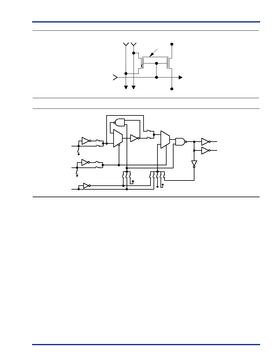
F l a s h S w i t c h
In the ProASIC Flash switch, two transistors share the
floating gate which stores the programming information.
One is the Flash transistor which stores programming
information and in which erasing is performed. The second
transistor connects/separates routing elements or
configuration signal lines (
Figure 2 on page 5
).
L o g i c T i l e
The logic tile cell,
Figure 3 on page 5
, has three inputs (any
or all of which can be inverted) and one output (which can
connect to both ultra fast local and efficient long line
routing resources). Any three-input one-output logic
function, except a three input XOR, can be configured as
one tile. Two multiplexers with feedback paths through the
NAND gates allow the tile to be configured as a latch with
clear or set, or as a flip-flop with clear or set. Thus, the tiles
can flexibly map logic and sequential gates of a design.
Figure 1 ∑ The ProASIC Device Architecture
256x9 Two-Port SRAM
or FIFO Block
Logic Tile
v3.0
5
P r o A S I C
TM
5 0 0 K F a m i l y
R o u ti n g R e s o u r c e s
The routing structure of the ProASIC 500K devices is
designed to provide high performance through a flexible
four-level hierarchy of routing resources: ultra fast local
resources, efficient long line resources, high speed very long
line resources, and high performance global networks.
The ultra fast local resources are dedicated lines that allow
the output of each tile to connect directly to every input of
the eight surrounding tiles (
Figure 4 on page 6
).
The efficient long line resources provide routing for longer
distances and higher fanout connections. These resources
vary in length (spanning 1, 2, or 4 tiles), run both vertically
and horizontally, and cover the entire ProASIC device
(
Figure 5 on page 6
). Each tile can drive signals onto the
efficient long line resources, while the resources can also
access every input of any tile. The routing software
automatically inserts active buffers to limit loading effects
due to distance and fanout.
The high speed very long line resources, spanning across
the entire device with minimal delay, are used to route very
long or very high fanout nets. These resources run vertically
and horizontally, providing multiple access to each group of
tiles throughout the device (
Figure 6 on page 7
).
The high performance global networks' clock trees are low
skew, high fanout nets that are accessible from four
dedicated pins or from internal logic (
Figure 7 on page 8
).
These nets are typically used to distribute clocks, resets,
and other high fanout nets requiring a minimum skew. The
global networks are implemented as clock trees, and signals
can be introduced at any junction. These can be employed
hierarchically, with signals accessing every input on all
tiles.
C l o c k R e s o u rc e s
ProASIC's high-drive routing structure provides four global
networks, each accessible from either a dedicated global
pad or a logic tile. Global lines provide optimized worst-case
clock skew of 0.3ns.
Figure 2 ∑ Flash Switch
Figure 3 ∑ Core Logic Tile
Sel 1
Sel 2
Switch In
Switch Out
Word
Floating Gate
Local Routing
In 1
In 2 (CLK)
In 3 (Reset)
Efficient Long
Line Routing