 | –≠–ª–µ–∫—Ç—Ä–æ–Ω–Ω—ã–π –∫–æ–º–ø–æ–Ω–µ–Ω—Ç: AD1992 | –°–∫–∞—á–∞—Ç—å:  PDF PDF  ZIP ZIP |

Class-D Audio Power Amplifier
Preliminary Technical Data
AD1990/AD1992/AD1994/AD1996
Rev. PrA ≠ 1/20/05
Information furnished by Analog Devices is believed to be accurate and reliable.
However, no responsibility is assumed by Analog Devices for its use, nor for any
infringements of patents or other rights of third parties that may result from its use.
Specifications subject to change without notice. No license is granted by implication
or otherwise under any patent or patent rights of Analog Devices. Trademarks and
registered trademarks are the property of their respective companies.
One Technology Way, P.O. Box 9106, Norwood, MA 02062-9106, U.S.A.
Tel: 781.329.4700
www.analog.com
Fax: 781.326.8703
© 2005 Analog Devices, Inc. All rights reserved.
FEATURES
Integrated Stereo Modulator & Power Stage
0.005% THD+N
101.5dB Dynamic Range
PSRR > 65 dB
R
DS-ON
< 0.3
(per transistor)
Efficiency > 80% @ 5W/6
EMI Optimized Modulator
On-Off-Mute Pop Noise Suppression
Short Circuit Protection
Over-Temperature Protection
Low Cost DMOS Process
APPLICATIONS
Flat Panel Televisions
Automotive Amplifiers
PC Audio Systems
Mini Components
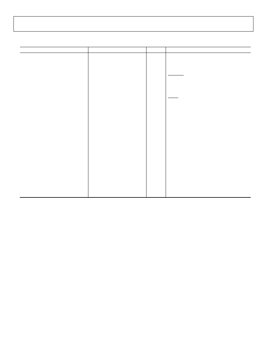
GENERAL DESCRIPTION
The AD199x is a two channel Bridge Tied Load (BTL)
switching audio power amplifier with integrated
modulator.
The modulator accepts a 1Vrms input signal (maximum power)
and generates a switching waveform to drive speakers directly.
One of the two modulators can control both output stages
providing twice the current for single-channel applications. A
digital, microcontroller-compatible interface provides control of
reset, mute and PGA gain as well as output signals for thermal
and over-current error conditions. The output stage can operate
from supply voltages ranging from 8V to 20V. The analog
modulator and digital logic operate from a 5V supply.
AD1990: 5Wx2 (10Wx1)
AD199
2: 10Wx2 (20Wx1)
AD199
4: 25Wx2 (50Wx1)
AD199
6: 40Wx2 (80Wx1)
PGND1
MODULATOR
PGA
LEFT CHANNEL
VOLTAGE
REFERENCE
OSCILLATOR
MODE CONTROL LOGIC
MUTE/
POP
CONTROL
TEMPERATURE
SENSE &
OVER-CURRENT
PROTECTION
19
E
R
R
0
29
M
U
T
E
17
E
R
R
2
30
R
S
T
/
P
W
D
N
49
M
O
N
O
18
E
R
R
1
7,8
4,5,6
1,2,3
9,10
11,12,13
14,15,16
55
27
28
22
21
20
41,42
43,44,45
46,47,48
39,40
36,37,38
33,34,35
50
51
60
53
31
32
62
63
PVDD
OUTL+
PGND1
PVDD1
OUTL-
PGND1
REF_FILT
CLKI
CLKO
D
C
T
R
L
0
D
C
T
R
L
1
D
C
T
R
L
2
PVDD2
OUTR+
PGND2
PVDD2
OUTR-
PGND2
N
F
R
+
N
F
R
-
N
F
L
+
N
F
L
-
P
G
A
0
P
G
A
1
A
I
N
L
A
I
N
R
AVDD
AGND
DVDD
DGND
57
56
24,25
23,26
ÿ1
ÿ2
ÿ1
ÿ2
PGND2
PVDD2
PVDD2
PGND2
LEVEL
SHIFT
+
DEAD
TIME
CONTROL
MODULATOR
PGA
RIGHT CHANNEL
DRIVER
HIGH SIDE
DRIVER
LOW SIDE
DRIVER
HIGH SIDE
DRIVER
LOW SIDE
DRIVER
HIGH SIDE
DRIVER
LOW SIDE
LEVEL
SHIFT
+
DEAD
TIME
CONTROL
Figure 1. Block Diagram

AD199x
Preliminary Technical Data
Rev. PrA ≠ 1/20/05 | Page 2 of 16
TABLE OF CONTENTS
General Description
........................................................................ 1
AD199x--Specifications.................................................................. 3
test conditions unless otherwise noted...................................... 3
Absolute Maximum Ratings............................................................ 6
Pin Configurations And Functional Descriptions ....................... 7
Typical Performance Characteristics ............................................. 8
Functional Description.................................................................. 10
Device Architecture ................................................................... 10
Amplifier Gain............................................................................ 10
System Design............................................................................. 11
Outline Dimensions ....................................................................... 14
ESD Caution................................................................................ 14

Preliminary Technical Data
AD199x
Rev. PrA ≠ 1/20/05 | Page 3 of 16
AD199X--SPECIFICATIONS
TEST CONDITIONS UNLESS OTHERWISE NOTED
Supply Voltages
AV
DD
5
V
DV
DD
5
V
PV
DDX
12
V
Ambient Temperature
25 ∞C
Load Impedance
6
Clock Frequency
11.2896 MHz
Measurement Bandwidth
20 Hz to 20 KHz
Table 1. Performance of both channels is identical
Parameter Min
Typ
Max
Units
Test
Conditions/Comments
OUTPUT POWER (P
O
)
AD1990
AD1992
AD1994
AD1996
4
5
8
10
16
25
25
40
W
W
W
W
W
W
W
W
R
L
= 6
, PV
DD
= 20 V, 1 kHz (FTC)
@ <0.01% THD+N
@ 10% THD+N (FTC)
@ <0.01% THD+N
@ 10% THD+N (FTC)
@ <0.01% THD+N
@ 10% THD+N (FTC)
@ <0.01% THD+N
@ 10% THD+N (FTC)
Efficiency
84
%
f
IN
=1 kHz, P
O
= 5 W, R
L
= 6
R
ON
per High Side Transistor
0.3
@ 1 A
per Low Side Transistor
0.2
@ 1 A
Maximum Current Through OUTx
4
A
Thermal Warning Active
135
∞C
Die temperature
Thermal Shutdown Active
150
∞C
Die temperature
Overcurrent Shutdown Active
4
A
Nominal Input Level
1.0
V
RMS
PGA gain = 0 dB
Modulation Factor
90
%
PERFORMANCE
SPECIFICATIONS
Total Harmonic Distortion (THD+N)
0.005
%
PGA = 0 dB, P
O
= 5 W
0.007
%
PGA = 6 dB, P
O
= 5 W
0.01
%
PGA = 12 dB, P
O
= 5 W
0.02
%
PGA = 18 dB, P
O
= 5 W
Signal/Noise Ratio (SNR)
102
dB
Dynamic Range (DNR)
102
dB
-60 dB Input
Crosstalk
Power supply rejection (PSRR)
60
45
-100
dB
dB
dB
Measured channel input = 0 V
RMS
,
other channel = 1 kHz at 5W
20 Hz - 1 kHz
20 Hz ≠ 20 kHz
DC
SPECIFICATIONS
Input
Impedance
20 k
AINL and AINR analog inputs
Output DC Offset Voltage
±10
mV
AD199x
Preliminary Technical Data
Rev. PrA ≠ 1/20/05 | Page 4 of 16
Parameter Min
Typ
Max
Units
Test
Conditions/Comments
POWER
SUPPLIES
Supply Voltage AV
DD
4.5 5 5.5 V
Supply Voltage DV
DD
4.5 5 5.5 V
Supply Voltage PV
DDX
6.5
8-20
22.5
V
Powerdown Current
RST/PDN held low
AV
DD
0.1
0.5
µA
DV
DD
0.1
0.5
µA
PV
DDX
19
25
µA
Mute
Current
MUTE held low
AV
DD
19 mA
DV
DD
2.7
mA
PVDD
1.5
mA
Quiesent Current
Inputs Grounded, Non-Overlap Time = TBD
AV
DD
20 mA
DV
DD
5.2
mA
PV
DDX
3.2
mA
Operating
Current
V
IN
= 1V
RMS
, P
O
= 5 W
AV
DD
22 mA
DV
DD
5.8
mA
PV
DD
4
A
per
FET
DIGITAL
I/O
Input Voltage High
2.0
DV
DD
V
Input Voltage Low
0.8
V
Output Voltage High
DV
DD
-0.8
V
@ 2 mA
Output Voltage Low
0.4
V
@ 2 mA
Leakage Current on Digital Inputs
10
µA
Preliminary Technical Data
AD199x
Rev. PrA ≠ 1/20/05 | Page 5 of 16
Table 2 DIGITAL TIMING (Guaranteed over -40∞C to +85∞C, AV
DD
= DV
DD
= 5.0V ± 10%, PV
DDX
=12V ± 10%, Non Overlap Time
t
NOL
= Shortest, See Table 6: Non-Overlap Time Settings)
Parameter Min
Typ
Max
Units
Comments
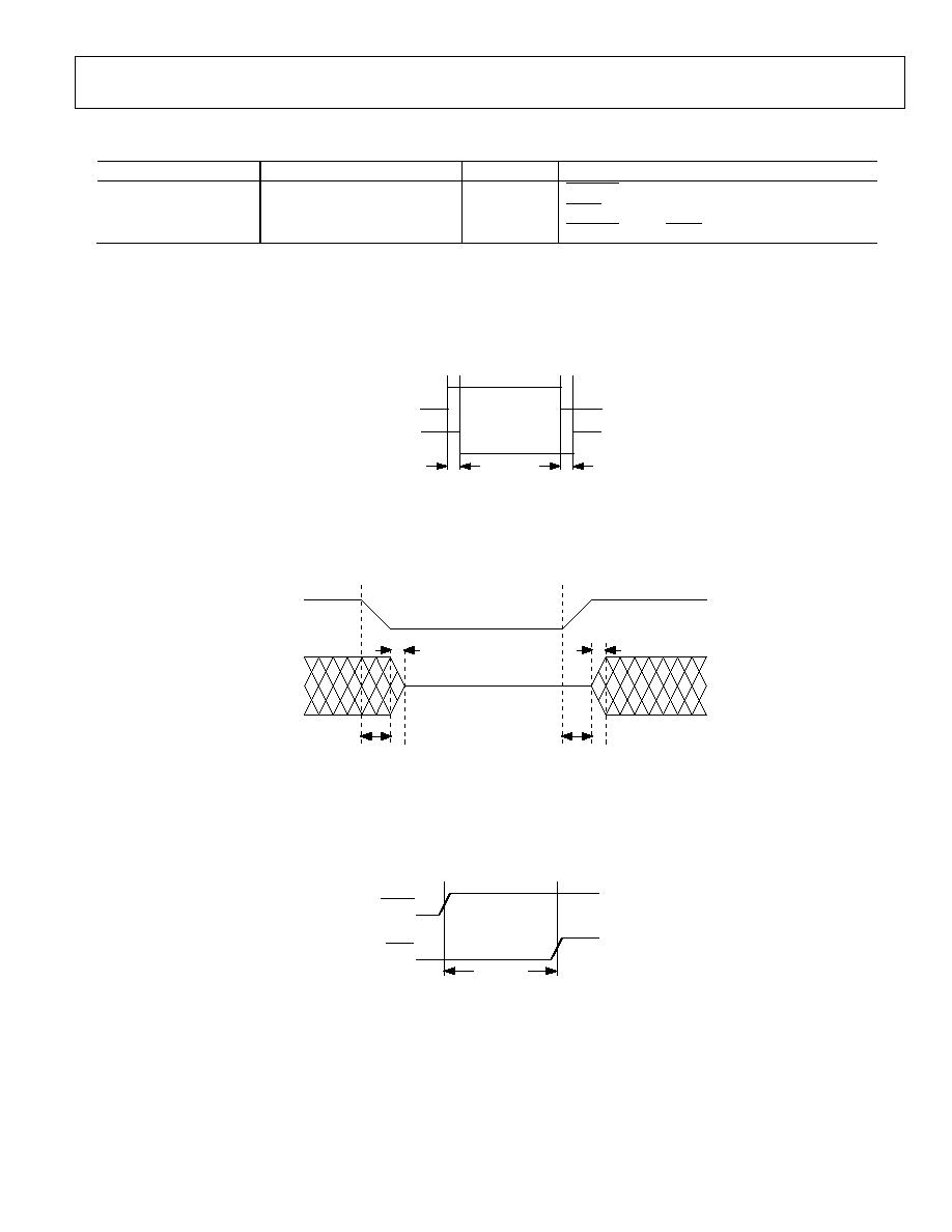
t
PDRP
500
ns
RST/PDN minimum low pulsewidth
t
MPDL
5 µs
MUTE asserted to output initial response
t
MUTEDLY
1
sec
RST/PDN high to MUTE high delay
t
NOL
OUTL+/
OUTR+
OUTL-/
OUTR-
t
NOL
Figure 2. Output Timing
OUTX
MUTE
tMPDL
tPST
tPST
tMPDL
Figure 3. Mute Timing
RESET
MUTE
t
MUTEDLY
Figure 4. Reset to Mute Delay