 | –≠–ª–µ–∫—Ç—Ä–æ–Ω–Ω—ã–π –∫–æ–º–ø–æ–Ω–µ–Ω—Ç: AD204 | –°–∫–∞—á–∞—Ç—å:  PDF PDF  ZIP ZIP |
FUNCTIONAL BLOCK DIAGRAM
a
Low Cost, Miniature
Isolation Amplifiers
AD202/AD204
REV. B
Information furnished by Analog Devices is believed to be accurate and
reliable. However, no responsibility is assumed by Analog Devices for its
use, nor for any infringements of patents or other rights of third parties
which may result from its use. No license is granted by implication or
otherwise under any patent or patent rights of Analog Devices.
FEATURES
Small Size: 4 Channels/lnch
Low Power: 35 mW (AD204)
High Accuracy:
±
0.025% max Nonlinearity (K Grade)
High CMR: 130 dB (Gain = 100 V/V)
Wide Bandwidth: 5 kHz Full-Power (AD204)
High CMV Isolation:
±
2000 V pk Continuous (K Grade)
(Signal and Power)
Isolated Power Outputs
Uncommitted Input Amplifier
APPLICATIONS
Multichannel Data Acquisition
Current Shunt Measurements
Motor Controls
Process Signal Isolation
High Voltage Instrumentation Amplifier
GENERAL DESCRIPTION
The AD202 and AD204 are general purpose, two-port, trans-
former-coupled isolation amplifiers that may be used in a broad
range of applications where input signals must be measured,
processed and/or transmitted without a galvanic connection.
These industry standard isolation amplifiers offer a complete
isolation function, with both signal and power isolation provided
for in a single compact plastic SIP or DIP style package. The
primary distinction between the AD202 and the AD204 is that
the AD202 is powered directly from a +15 V dc supply while
the AD204 is powered by an externally supplied clock, such as
the recommended AD246 Clock Driver.
The AD202 and AD204 provide total galvanic isolation between
the input and output stages of the isolation amplifier through
the use of internal transformer-coupling. The functionally com-
plete AD202 and AD204 eliminate the need for an external,
user-supplied dc/dc converter. This permits the designer to
minimize the necessary circuit overhead and consequently re-
duce the overall design and component costs.
The design of the AD202 and AD204 emphasizes maximum
flexibility and ease of use, including the availability of an un-
committed op amp on the input stage. They feature a bipolar
±
5 V output range, an adjustable gain range of from 1 to 100 V/V,
±
0.025% max nonlinearity (K grade), 130 dB of CMR and the
AD204 consumes a low 35 mW of power.
PRODUCT HIGHLIGHTS
The AD202 and AD204 are full-featured isolators offering
numerous benefits to the user:
Small Size:
The AD202 and AD204 are available in SIP and
DIP form packages. The SIP package is just 0.25" wide, giving
the user a channel density of four channels per inch. The
isolation barrier is positioned to maximize input to output spac-
ing. For applications requiring a low profile, the DIP package
provides a height of just 0.350".
High Accuracy:
With a maximum nonlinearity of
±
0.025%
for the AD202K/AD204K (
±
0.05% for the AD202J/AD204J)
and low drift over temperature, the AD202 and AD204 provide
high isolation without loss of signal integrity.
Low Power:
Power consumption of 35 mW (AD204) and
75 mW (AD202) over the full signal range makes these isolators
ideal for use in applications with large channel counts or tight
power budgets.
Wide Bandwidth:
The AD204's full-power bandwidth of
5 kHz makes it useful for wideband signals. It is also effective in
applications like control loops, where limited bandwidth could
result in instability.
Excellent Common-Mode Performance:
The AD202K/
AD204K provide
±
2000 V pk continuous common-mode isola-
tion, while the AD202J/AD204J provide
±
1000 V pk continuous
common-mode isolation. All models have a total common-mode
input capacitance of less than 5 pF inclusive of power isolation.
This results in CMR ranging from 130 dB at a gain of 100 dB to
104 dB (minimum at unity gain) and very low leakage current
(2
µ
A maximum).
Flexible Input:
An uncommitted op amp is provided at the
input of all models. This provides buffering and gain as required,
and facilitates many alternative input functions including filter-
ing, summing, high-voltage ranges, and current (transimped-
ance) input.
Isolated Power:
The AD204 can supply isolated power of
±
7.5 V at 2 mA. This is sufficient to operate a low-drift input
preamp, provide excitation to a semiconductor strain gage, or to
power any of a wide range of user-supplied ancillary circuits.
The AD202 can supply
±
7.5 V at 0.4 mA which is sufficient to
operate adjustment networks or low-power references and op
amps, or to provide an open-input alarm.
© Analog Devices, Inc., 1994
One Technology Way, P.O. Box 9106, Norwood. MA 02062-9106, U.S.A.
Tel: 617/329-4700
Fax: 617/326-8703
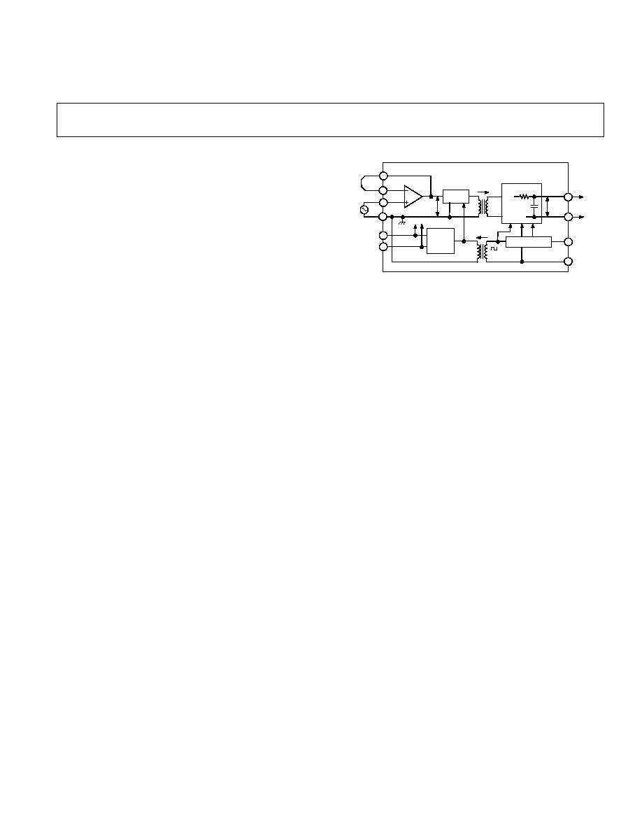
MOD
RECT &
FILTER
3
2
V
SIG
1
4
SIGNAL
DEMOD
±
5V
F.S.
25kHz
25kHz
POWER
OSCILLATOR
FB
IN≠
IN+
IN COM
38
37
31
32
POWER
RETURN
+15V DC
V
OUT
HI
LO
AD202
+7.5V
≠7.5V
≠V
ISO
OUT
+V
ISO
OUT
±
5V
FS
6
5

REV. B
≠2≠
(typical @ + 25
∞
C & V
S
= +15 V unless otherwise noted)
AD202/AD204≠SPECIFICATIONS
Model
AD204J
AD204K
AD202J
AD202K
GAIN
Range
1 V/V≠100 V/V
*
*
*
Error
±
0.5% typ (
±
4% max)
*
*
*
vs. Temperature
±
20 ppm/
∞
C typ (
±
45 ppm/
∞
C max) *
*
*
vs. Time
±
50 ppm/1000 Hours
*
*
*
vs. Supply Voltage
±
0.01%/V
±
0.01%/V
±
0.01%/V
±
0.01%/V
Nonlinearity (G = 1 V/V)
1
±
0.05% max
±
0.025% max
±
0.05% max
±
0.025% max
Nonlinearity vs. Isolated Supply Load
±
0.0015%/mA
*
*
*
INPUT VOLTAGE RATINGS
Input Voltage Range
±
5 V
*
*
*
Max lsolation Voltage (Input to Output)
AC, 60 Hz, Continuous
750 V rms
1500 V rms
750 V rms
1500 V rms
Continuous (AC and DC)
±
1000 V Peak
±
2000 V Peak
±
1000 V Peak
±
2000 V Peak
Isolation-Mode Rejection Ratio (IMRR) @ 60 Hz
R
S
100
(HI & LO lnputs) G = 1 V/V
110 dB
110 dB
105 dB
105 dB
G = 100 V/V
130 dB
*
*
*
R
S
l k
(Input HI, LO, or Both) G = 1 V/V
104 dB min
104 dB min
100 dB min
100 dB min
G = 100 V/V
110 dB min
*
*
*
Leakage Current Input to Output @ (240 V rms, 60 Hz 2
µ
A rms max
*
*
*
INPUT IMPEDANCE
Differential (G = 1 V/V)
10
12
*
*
*
Common Mode
2 G
4.5 pF
*
*
*
INPUT BIAS CURRENT
Initial, @ +25
∞
C
±
30 pA
*
*
*
vs. Temperature (0
∞
C to +70
∞
C)
±
10 nA
*
*
*
INPUT DIFFERENCE CURRENT
Initial, @ +25
∞
C
±
5 pA
*
*
*
vs. Temperature (0
∞
C to +70
∞
C)
±
2 nA
*
*
*
INPUT NOISE
Voltage, 0.1 Hz to 100 Hz
4
µ
V p-p
*
*
*
f > 200 Hz
50 nV/
Hz
*
*
*
FREQUENCY RESPONSE
Bandwidth (V
O
10 V p-p, G = 1 V≠50 V/V)
5 kHz
5 kHz
2 kHz
2 kHz
Settling Time, to
±
10 mV (10 V Step)
1 ms
*
*
*
OFFSET VOLTAGE (RTI)
Initial, @ +25
∞
C Adjustable to Zero
(
±
15
±
15/G)mV max
(
±
5
±
5/G)mVmax
(
±
15
±
15/G)mVmax
(
±
5
±
5/G)mVmax
vs . Temperature (0
∞
C to +70
∞
C)
±
10
±
10
G
µ
V/
∞
C
RATED OUTPUT
Voltage (Out HI to Out LO)
±
5 V
*
*
*
Voltage at Out HI or Out LO (Ref. Pin 32)
±
6.5 V
*
*
*
Output Resistance
3 k
3 k
7 k
7 k
Output Ripple, 100 kHz Bandwidth
10 mV pk-pk
*
*
*
5 kHz Bandwidth
0.5 mV rms
*
*
*
ISOLATED POWER OUTPUT
2
Voltage, No Load
±
7.5 V
*
*
*
Accuracy
±
10%
*
*
*
Current
2 mA (Either Output)
3
2 mA (Either Output)
3
400
µ
A Total
400
µ
A Total
Regulation, No Load to Full Load
5%
*
*
*
Ripple
100 mV pk-pk
*
*
*
OSCILLATOR DRIVE INPUT
Input Voltage
15 V pk-pk Nominal
15 V pk-pk Nominal
N/A
N/A
Input Frequency
25 kHz Nominal
25 kHz Nominal
N/A
N/A
POWER SUPPLY (AD202 Only)
Voltage, Rated Performance
N/A
N/A
+15 V
±
5%
+15 V
±
5%
Voltage, Operating
N/A
N/A
+15 V
±
10%
+15 V
±
10%
Current, No Load (V
S
= +15 V)
N/A
N/A
5 mA
5 mA
TEMPERATURE RANGE
Rated Performance
0
∞
C to +70
∞
C
*
*
*
Operating
≠40
∞
C to +85
∞
C
*
*
*
Storage
≠40
∞
C to +85
∞
C
*
*
*
PACKAGE DIMENSIONS
4
SIP Package (Y)
2.08"
◊
0.250"
◊
0.625"
*
*
*
DlP Package
(N)
2.10"
◊
0.700"
◊
0.350"
*
*
*
NOTES
Specifications same as AD204J.
1
Nonlinearity is specified as a % deviation from a best straight line.
2
1.0
µ
F min decoupling required (see text).
3
3 mA with one supply loaded.
4
Width is 0.25" typ, o.26" max.
Specifications subject to change without notice .
AD202/AD204
REV. B
≠3≠
PIN DESIGNATIONS
AD202/AD204 SIP Package
Pin
Function
1
+INPUT
2
INPUT/V
ISO
COMMON
3
≠INPUT
4
INPUT FEEDBACK
5
≠V
ISO
OUTPUT
6
+V
ISO
OUTPUT
31
+15 V POWER IN (AD202 ONLY)
32
CLOCK/POWER COMMON
33
CLOCK INPUT (AD204 ONLY)
37
OUTPUT LO
38
OUTPUT HI
AD202/AD204 DIP Package
Pin
Function
1
+INPUT
2
INPUT/V
ISO
COMMON
3
≠INPUT
18
OUTPUT LO
19
OUTPUT HI
20
+15 V POWER IN (AD202 ONLY)
21
CLOCK INPUT (AD204 ONLY)
22
CLOCK/POWER COMMON
36
+V
ISO
OUTPUT
37
≠V
ISO
OUTPUT
38
INPUT FEEDBACK
AD246≠SPECIFICATIONS
(typical @ +25
∞
C & V
S
= +15 V unless otherwise noted)
Model
AD246JY
AD246JN
OUTPUT
l
Frequency
25 kHz Nominal
*
Voltage
15 V p-p Nominal *
Fan-Out
32 max
*
POWER SUPPLY
REQUIREMENTS
Input Voltage
+15 V
±
5%
*
Supply Current
Unloaded
35 mA
*
Each AD204 Adds
2.2 mA
*
Each 1 mA Load on AD204
+V
ISO
or ≠V
ISO
Adds
0.7 mA
*
NOTES
*Specifications the same as the AD246JY.
1
The high current drive output will not support a short to ground.
Specifications subject to change without notice.
AD246 Pin Designations
Pin (Y)
Pin (N)
Function
1
12
+15 V POWER IN
2
1
CLOCK OUTPUT
12
14
COMMON
13
24
COMMON
ORDERING GUIDE
Package
Max Common-
Max
Model
Option
Mode Voltage (Peak)
Linearity
AD202JY
SIP
1000 V
±
0.05%
AD202KY
SIP
2000 V
±
0.025%
AD202JN
DIP
1000 V
±
0.05%
AD202KN
DIP
2000 V
±
0.025%
AD204JY
SIP
1000 V
±
0.05%
AD204KY
SIP
2000 V
±
0.025%
AD204JN
DIP
1000 V
±
0.05%
AD204KN
DIP
2000 V
±
0.025%
WARNING!
ESD SENSITIVE DEVICE
CAUTION
ESD (electrostatic discharge) sensitive device. Electrostatic charges as high as 4000 V readily
accumulate on the human body and test equipment and can discharge without detection.
Although the AD202/AD204 features proprietary ESD protection circuitry, permanent damage
may occur on devices subjected to high energy electrostatic discharges. Therefore, proper ESD
precautions are recommended to avoid performance degradation or loss of functionality.

REV. B
≠4≠
AD202/AD204
DIFFERENCES BETWEEN THE AD202 AND AD204
The primary distinction between the AD202 and AD204 is in
the method by which they are powered: the AD202 operates
directly from +15 V dc while the AD204 is powered by a non-
isolated externally-supplied clock (AD246) which can drive up
to 32 AD204s. The main advantages of using the externally-
clocked AD204 over the AD202 are reduced cost in multichannel
applications, lower power consumption, and higher bandwidth.
In addition, the AD204 can supply substantially more isolated
power than the AD202.
Of course, in a great many situations, especially where only one
or a few isolators are used, the convenience of stand-alone op-
eration provided by the AD202 will be more significant than any
of the AD204's advantages. There may also be cases where it is
desirable to accommodate either device interchangeably, so the
pinouts of the two products have been designed to make that
easy to do.
MOD
RECT &
FILTER
3
2
V
SIG
1
4
SIGNAL
DEMOD
±
5V
F.S.
25kHz
25kHz
POWER
OSCILLATOR
FB
IN≠
IN+
IN COM
38
37
31
32
POWER
RETURN
+15V DC
V
OUT
HI
LO
AD202
+7.5V
≠7.5V
≠V
ISO
OUT
+V
ISO
OUT
±
5V
FS
6
5
Figure 1a. AD202 Functional Block Diagram
MOD
RECT &
FILTER
3
2
V
SIG
1
4
SIGNAL
±
5V
F.S.
25kHz
25kHz
POWER
FB
IN≠
IN+
IN COM
33
32
POWER
RETURN
(15V
p-p/25kHz)
V
OUT
HI
LO
AD204
+7.5V
≠7.5V
≠V
ISO
OUT
+V
ISO
OUT
±
5V
FS
6
5
CLOCK
POWER
CONV.
DEMOD
38
37
Figure 1b. AD204 Functional Block Diagram
(Pin Designations Apply to the DIP-Style Package)
INSIDE THE AD202 AND AD204
The AD202 and AD204 use an amplitude modulation technique
to permit transformer coupling of signals down to dc (Figure 1a
and 1b). Both models also contain an uncommitted input op
amp and a power transformer which provides isolated power to
the op amp, the modulator, and any external load. The power
transformer primary is driven by a 25 kHz, 15 V p-p square
wave which is generated internally in the case of the AD202, or
supplied externally for the AD204.
Within the signal swing limits of approximately
±
5 V, the output
voltage of the isolator is equal to the output voltage of the op
amp; that is, the isolation barrier has unity gain. The output sig-
nal is not internally buffered, so the user is free to interchange
the output leads to get signal inversion. Additionally, in multi-
channel applications, the unbuffered outputs can be multiplexed
with one buffer following the mux. This technique minimizes
offset errors while reducing power consumption and cost. The
(Circuit figures shown on this page are for SIP style pack-
ages. Refer to page 3 for proper DIP package pinout.)
output resistance of the isolator is typically 3 k
for the AD204
(7 k
for AD202) and varies with signal level and temperature,
so it should not be loaded (see Figure 2 for the effects of load
upon nonlinearity and gain drift). In many cases a high-imped-
ance load will be present or a following circuit such as an output
filter can serve as a buffer, so that a separate buffer function will
not often be needed.
Figure 2. Effects of Output Loading
USING THE AD202 AND AD204
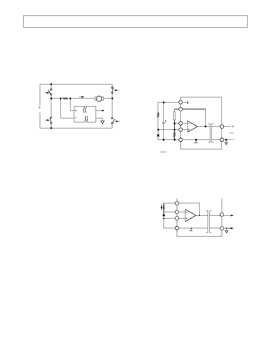
Powering the AD202.
The AD202 requires only a single +15 V
power supply connected as shown in Figure 3a. A bypass ca-
pacitor is provided in the module.
Figure 3a.
Powering the AD204.
The AD204 gets its power from an ex-
ternally supplied clock signal (a 15 V p-p square wave with a
nominal frequency of 25 kHz) as shown in Figure 3b.
Figure 3b.
AD246 Clock Driver.
The AD246 is a compact, inexpensive
clock driver that can be used to obtain the required clock from a
single 15 V supply. Alternatively, the circuit shown in Figure 4
(essentially an AD246) can be used. In either case, one clock
circuit can operate at least 32 AD204s at the rated minimum
supply voltage of 14.25 V and one additional isolator can be
operated for each 40 mV increase in supply voltage up to 15 V.
A supply bypass capacitor is included in the AD246, but if many

AD202/AD204
REV. B
≠5≠
The "noninverting" circuit of Figures 5 and 6 can also be used
to advantage when a signal inversion is needed: just interchange
either the input leads or the output leads to get inversion. This
approach retains the high input resistance of the "noninverting"
circuit, and at unity gain no gain-setting resistors are needed.
When the isolator is not powered, a negative input voltage of
more than about 2 V will cause an input current to flow. If the
signal source can supply more than a few mA under such condi-
tions, the 2 k
resistor shown in series with IN+ should be used
to limit current to a safe value. This is particularly important
with the AD202, which may not start if a large input current is
present.
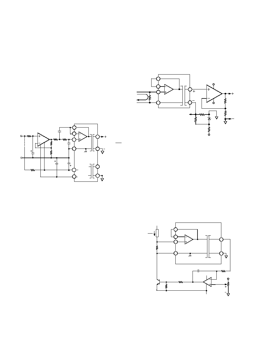
Figure 7 shows how to accommodate current inputs or sum cur-
rents or voltages. This circuit can also be used when the input
signal is larger than the
±
5 V input range of the isolator; for
example, a
±
50 V input span can be accommodated with R
F
=
20 k and R
S
= 200 k. Once again, a capacitor from FB to IN
COM is required for gains above five.
Figure 7. Connections for Summing or Current Inputs
Adjustments.
When gain and zero adjustments are needed, the
circuit details will depend on whether adjustments are to be
made at the isolator input or output, and (for input adjust-
ments) on the input circuit used. Adjustments are usually best
done on the input side, because it is better to null the zero
ahead of the gain, and because gain adjustment is most easily
done as part of the gain-setting network. Input adjustments are
also to be preferred when the pots will be near the input end of
the isolator (to minimize common-mode strays). Adjustments
on the output side might be used if pots on the input side would
represent a hazard due to the presence of large common-mode
voltages during adjustment.
Figure 8a shows the input-side adjustment connections for use
with the "noninverting" connection of the input amplifier. The
zero adjustment circuit injects a small adjustment voltage in
series with the low side of the signal source. (This will not work
if the source has another current path to input common or if
current flows in the signal source LO lead). Since the adjust-
ment voltage is injected ahead of the gain, the values shown will
(Circuit figures shown on this page are for SIP style pack-
ages. Refer to Page 3 for proper DIP package pinout.)
AD204s are operated from a single AD246, an external bypass
capacitor should be used with a value of at least 1
µ
F for every
five isolators used. Place the capacitor as close as possible to the
clock driver.
Figure 4. Clock Driver
Input Configurations.
The AD202 and AD204 have been de-
signed to be very easy to use in a wide range of applications.
The basic connection for standard unity gain applications, useful
for signals up to
±
5 V, is shown in Figure 5; some of the possible
variations are described below. When smaller signals must be
Figure 5. Basic Unity-Gain Application
handled, Figure 6 shows how to get gain while preserving a very
high input resistance. The value of feedback resistor R
F
should
be kept above 20 k
for best results. Whenever a gain of more
than five is taken, a 100 pF capacitor from FB to IN COM is
required. At lower gains this capacitor is unnecessary, but it will
not adversely affect performance if used.
Figure 6. Input Connections for Gain > 1
REV. B
≠6≠
AD202/AD204
work for any gain. Keep the resistance in series with input LO
below a few hundred ohms to avoid CMR degradation.
Figure 8a. Adjustments for Noninverting Connection of
Op Amp
Also shown in Figure 8a is the preferred means of adjusting the
gain-setting network. The circuit shown gives a nominal R
F
of
50 k
, and will work properly for gains of ten or greater. The
adjustment becomes less effective at lower gains (its effect is
halved at G = 2) so that the pot will have to be a larger fraction
of the total R
F
at low gain. At G = 1 (follower) the gain cannot
be adjusted downward without compromising input resistance;
it is better to adjust gain at the signal source or after the output.
Figure 8b shows adjustments for use with inverting input cir-
cuits. The zero adjustment nulls the voltage at the summing
node. This method is preferable to current injection because it is
less affected by subsequent gain adjustment. Gain adjustment is
again done in the feedback; but in this case it will work all the
way down to unity gain (and below) without alteration.
Figure 8b. Adjustments for Summing or Current Input
Figure 9 shows how zero adjustment is done at the output by
taking advantage of the semi-floating output port. The range of
this adjustment will have to be increased at higher gains; if that
is done, be sure to use a suitably stable supply voltage for the
pot circuit.
There is no easy way to adjust gain at the output side of the iso-
lator itself. If gain adjustment must be done on the output side,
it will have to be in a following circuit such as an output buffer
or filter.
Figure 9. Output-Side Zero Adjustment
Common-Mode Performance.
Figures 10a and 10b show
how the common-mode rejection of the AD202 and AD204 var-
ies with frequency, gain, and source resistance. For these isola-
tors, the significant resistance will normally be that the path
from the source of the common-mode signal to IN COM. The
AD202 and AD204 also perform well in applications requiring
rejection of fast common-mode steps, as described in the Appli-
cations section.
Figure 10a. AD204
(Circuit figures shown on this page are for SIP style pack-
ages. Refer to page 3 for proper DIP package pinout.)
AD202/AD204
REV. B
≠7≠
Figure 10b. AD202
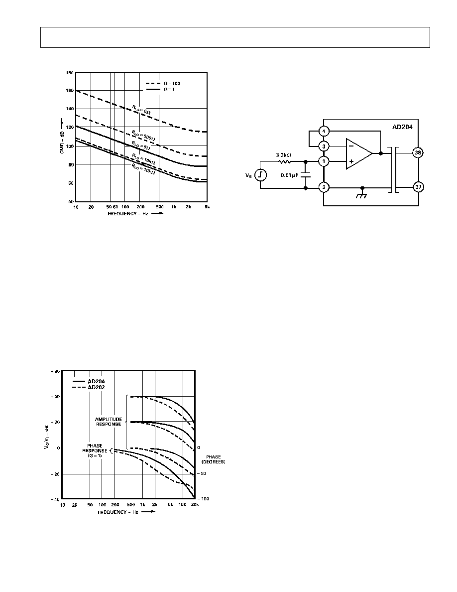
Dynamics and Noise.
Frequency response plots for the
AD202 and AD204 are given in Figure 11. Since neither isola-
tor is slew-rate limited, the plots apply for both large and small
signals. Capacitive loads of up to 470 pF will not materially af-
fect frequency response. When large signals beyond a few hun-
dred Hz will be present, it is advisable to bypass ≠V
ISO
and
+V
ISO
to IN COM with 1
µ
F tantalum capacitors even if the
isolated supplies are not loaded.
At 50 Hz/60 Hz, phase shift through the AD202/AD204 is
typically 0.8
∞
(lagging). Typical unit--unit variation is
±
0.2
∞
(lagging).
Figure 11. Frequency Response at Several Gains
The step response of the AD204 for very fast input signals can
be improved by the use of an input filter, as shown in Figure 12.
The filter limits the bandwidth of the input (to about 5.3 kHz)
so that the isolator does not see fast, out-of-band input terms
that can cause small amounts (
±
0.3%) of internal ringing. The
AD204 will then settle to
±
0.1% in about 300 microseconds for
a 10 V step.
Figure 12. Input Filter for Improved Step Response
Except at the highest useful gains, the noise seen at the output
of the AD202 and AD204 will be almost entirely comprised of
carrier ripple at multiples of 25 kHz. The ripple is typically
2 mV p-p near zero output and increases to about 7 mV p-p for
outputs of
±
5 V (1 MHz measurement bandwidth). Adding a
capacitor across the output will reduce ripple at the expense of
bandwidth: for example, 0.05
µ
F at the output of the AD204
will result in 1.5 mV ripple at
±
5 V, but signal bandwidth will
be down to 1 kHz.
When the full isolator bandwidth is needed, the simple two-pole
active filter shown in Figure 13 can be used. It will reduce ripple
to 0.1 mV p-p with no loss of signal bandwidth, and also serves
as an output buffer.
An output buffer or filter may sometimes show output spikes
that do not appear at its input. This is usually due to clock noise
appearing at the op amp's supply pins (since most op amps have
little or no supply rejection at high frequencies). Another com-
mon source of carrier-related noise is the sharing of a ground
track by both the output circuit and the power input. Figure 13
shows how to avoid these problems: the clock/supply port of the
isolator does not share ground or 15 V tracks with any signal
circuits, and the op amp's supply pins are bypassed to signal
common (note that the grounded filter capacitor goes here as
well). Ideally, the output signal LO lead and the supply com-
mon meet where the isolator output is actually measured, e.g.,
at an A/D converter input. If that point is more than a few feet
from the isolator, it may be useful to bypass output LO to sup-
ply common at the isolator with a 0.1
µ
F capacitor.
In applications where more than a few AD204s are driven by a
single clock driver, substantial current spikes will flow in the
power return line and in whichever signal out lead returns to a
low impedance point (usually output LO). Both of these tracks
(Circuit figures shown on this page are for SIP style pack-
ages. Refer to page 3 for proper DIP package pinout.)

REV. B
≠8≠
AD202/AD204
should be made large to minimize inductance and resistance;
ideally, output LO should be directly connected to a ground
plane which serves as measurement common.
Current spikes can be greatly reduced by connecting a small in-
ductance (68
µ
H≠100
µ
H) in series with the clock pin of each
AD204. Molded chokes such as the Dale IM-2 series, with dc
resistance of about 5
, are suitable.
Figure 13. Output Filter Circuit Showing Proper Grounding
Using Isolated Power.
Both the AD202 and the AD204 pro-
vide
±
7.5 V power outputs referenced to input common. These
may be used to power various accessory circuits which must
operate at the input common-mode level; the input zero adjust-
ment pots described above are an example, and several other
possible uses are shown in the section titled Application
Examples.
The isolated power output of the AD202 (400
µ
A total from ei-
ther or both outputs) is much more limited in current capacity
than that of the AD204, but it is sufficient for operating mi-
cropower op amps, low power references (such as the AD589),
adjustment circuits, and the like.
The AD204 gets its power from an external clock driver, and
can handle loads on its isolated supply outputs of 2 mA for each
supply terminal ( +7.5 V and ≠7.5 V) or 3 mA for a single
loaded output. Whenever the external load on either supply is
more than about 200
µ
A, a 1
µ
F tantalum capacitor should be
used to bypass each loaded supply pin to input common.
(Circuit figures shown on this page are for SIP style pack-
ages. Refer to page 3 for proper DIP package pinout.)
Up to 32 AD204s can be driven from a single AD246 (or
equivalent) clock driver when the isolated power outputs of the
AD204s are loaded with less than 200
µ
A each, at a worst-case
supply voltage of 14.25 V at the clock driver. The number of
AD204s that can be driven by one clock driver is reduced by
one AD204 per 3.5 mA of isolated power load current at 7.5 V,
distributed in any way over the AD204s being supplied by that
clock driver. Thus a load of 1.75 mA from +V
ISO
to ≠V
ISO
would
also count as one isolator because it spans 15 V.
It is possible to increase clock fanout by increasing supply volt-
age above the 14.25 V minimum required for 32 loads. One ad-
ditional isolator (or 3.5 mA unit load) can be driven for each
40 mV of increase in supply voltage up to 15 V. Therefore if the
minimum supply voltage can be held to 15 V ≠ 1%, it is possible
to operate 32 AD204s and 52 mA of 7.5 V loads. Figure 14
shows the allowable combinations of load current and channel
count for various supply voltages.
Figure 14. AD246 Fanout Rules
AD202/AD204
REV. B
≠9≠
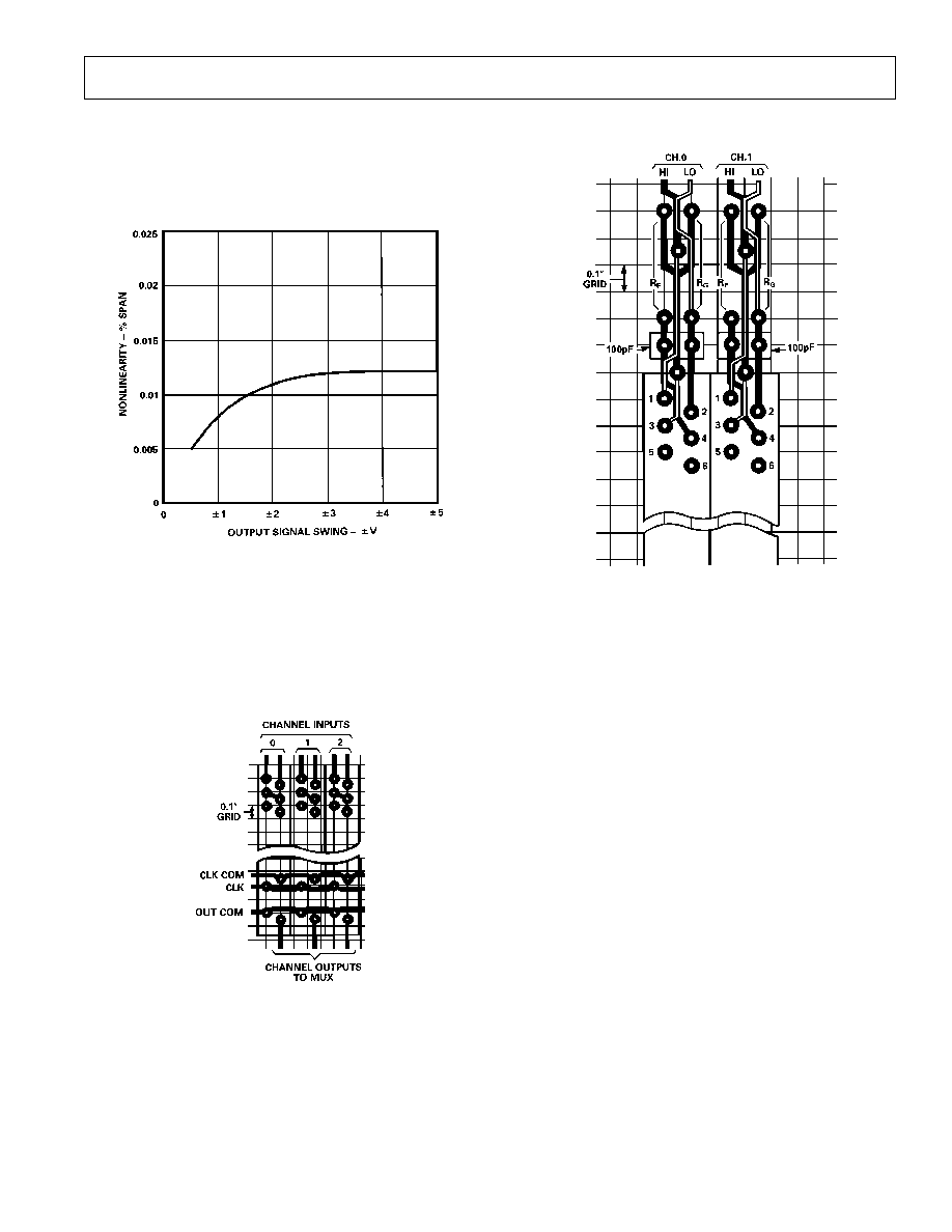
Operation at Reduced Signal Swing.
Although the nominal
output signal swing for the AD202 and AD204 is
±
5 V, there
may be cases where a smaller signal range may be desirable.
When that is done, the fixed errors (principally offset terms and
output noise) become a larger fraction of the signal, but nonlin-
earity is reduced. This is shown in Figure 15.
Figure 15. Nonlinearity vs. Signal Swing
PCB
Layout for Multichannel Applications. The pinout of
the AD204Y has been designed to make very dense packing
possible in multichannel applications. Figure 16a shows the rec-
ommended printed circuit board (PCB) layout for the simple
voltage-follower connection. When gain-setting resistors are
present, 0.25" channel centers can still be achieved, as shown in
Figure 16b.
Figure 16a.
Figure 16b.
(Circuit figures shown on this page are for SIP style pack-
ages. Refer to page 3 for proper DIP package pinout.)
REV. B
≠10≠
AD202/AD204
Process Current Input with Offset.
Figure 18 shows an iso-
lator receiver which translates a 4-20 mA process current signal
into a 0 V to +10 V output. A 1 V to 5 V signal appears at the
isolator's output, and a ≠1 V reference applied to output LO
provides the necessary level shift (in multichannel applications,
the reference can be shared by all channels). This technique is
often useful for getting offset with a follower-type output buffer.
4
37
38
3
2
≠15V
+15V
15k
10k
0 TO +10V
6
4
7
1
2
250
AD202
OR
AD204
1V TO 5V
3
4-20mA
≠1V TO
ADDITIONAL
CHANNELS
1k
≠15V
AD589
237
6.8k
Figure 18. Process Current Input Isolator with Offset
The circuit as shown requires a source compliance of at least
5 V, but if necessary that can be reduced by using a lower value
of current-sampling resistor and configuring the input amplifier
for a small gain.
High-Compliance Current Source.
In Figure 19, an isolator
is used to sense the voltage across current-sensing resistor R to
allow direct feedback control of a high-voltage transistor or FET
used as a high-compliance current source. Since the isolator has
virtually no response to dc common-mode voltage, the closed-
loop current source has a static output resistance greater than
10
14
even for output currents of several mA. The output cur-
rent capability of the circuit is limited only by power dissipation
in the source transistor.
4
3
1
AD202
OR
AD204
38
37
~
LOAD
I
L
= V
C
R
S
≠10V TO +250V
100k
470pF
~
+15V
+5V REF
20k
V
C
~
≠15V
10k
1k
MPS
U10
R
S
1k
2
Figure 19. High-Compliance Current Source
Synchronization.
Since AD204s operate from a common
clock, synchronization is inherent. AD202s will normally not in-
teract to produce beat frequencies even when mounted on 0.25-
inch centers. Interaction may occur in rare situations where a
large number of long, unshielded input cables are bundled to-
gether and channel gains are high. In such cases, shielded cable
may be required or AD204s can be used.
APPLICATIONS EXAMPLES
Low-Level Sensor Inputs.
In applications where the output
of low-level sensors such as thermocouples must be isolated, a
low drift input amplifier can be used with an AD204, as shown
in Figure 17. A three-pole active filter is included in the design
to get normal-mode rejection of frequencies above a few Hz and
to provide enhanced common-mode rejection at 60 Hz. If offset
adjustment is needed, it is best done at the trim pins of the
OP07 itself; gain adjustment can be done at the feedback
resistor.
3
1
0.15µF
33
32
4
~
~
470k
470k
CLK RET
CLK
37
6
2
0.039µF
38
V
O
= V
I
x 1 + 50k
R
G
(
)
5
1µF
1µF
R
G
49.9k
4
7
2
3
6
39k
220M
OPTIONAL
OPEN INPUT
DETECTION
AD204
+7.5V
≠7.5V
HI
LO
1µF
AD OP-07
Figure 17. Input Amplifier & Filter for Sensor Signals
Note that the isolated supply current is large enough to mandate
the use of 1
µ
F supply bypass capacitors. This circuit can be
used with an AD202 if a low-power op amp is used instead of
the OP07.
(Circuit figures shown on this page are for SIP style pack-
ages. Refer to page 3 for proper DIP package pinout.)
AD202/AD204
REV. B
≠11≠
Motor Control Isolator.
The AD202 and AD204 perform
very well in applications where rejection of fast common-mode
steps is important but bandwidth must not be compromised.
Current sensing in a fill-wave bridge motor driver (Figure 20) is
one example of this class of application. For 200 V common-
mode steps (1
µ
s rise time) and a gain of 50 as shown, the typi-
cal response at the isolator output will be spikes of
±
5 mV
amplitude, decaying to zero in less than 100
µ
s. Spike height can
be reduced by a factor of four with output filtering just beyond
the isolator's bandwidth.
AD204
M
±
20A
200V dc
±
5V
±
100mV
5m
Figure 20. Motor Control Current Sensing
Floating Current Source/Ohmmeter.
When a small floating
current is needed with a compliance range of up to
±
1000 V dc,
the AD204 can be used to both create and regulate the current.
This can save considerable power, since the controlled current
does not have to return to ground. In Figure 21, an AD589 ref-
erence is used to force a small fixed voltage across R. That sets
the current which the input op amp will have to return through
the load to zero its input. Note that the isolator's output isn't
needed at all in this application; the whole job is done by the in-
put section. However, the signal at the output could be useful
it's the voltage across the load, referenced to ground. Since the
load current is known, the output voltage is proportional to load
resistance.
3
37
38
AD204
V
O
= x R
L
V
R
R
4
LOAD
1
2
6
1µF
+7.5V
30k
AD589
R
I
LOAD
= (2mA MAX)
1.23V
R
V
LOAD
4V
Figure 21. Floating Current Source
Photodiode Amplifier.
Figure 22 shows a transresistance con-
nection used to isolate and amplify the output of a photodiode.
The photodiode operates at zero bias, and its output current is
scaled by R
F
to give a +5 V full-scale output.
1
AD202
OR
AD204
38
37
4
3
500k
2
PHOTO
DIODE
0 TO +5V
10µA
FS
Figure 22. Photodiode Amplifier
(Circuit figures shown on this page are for SIP style pack-
ages. Refer to page 3 for proper DIP package pinout.)

REV. B
≠12≠
AD202/AD204
OUTLINE DIMENSIONS
Dimensions shown in inches and (mm).
PRINTED IN U.S.A.
C946e≠5≠12/94
AD202/AD204 SIP Package
0.15
(3.81)
TYP
1
3
5
2
6
31 33
37
38
32
4
0.05 (1.3)TYP
1.30 (33.0)
0.010 x 0.020
(0.25 x 0.51)
0.20
(5.1)
0.143
(3.63)
0.625
(15.9)
MAX
0.12
(3.05)
0.10 (2.5)
TYP
0.250 (6.3) TYP
0.260 (6.6) MAX
2.08 (52.8) MAX
FRONT VIEW
BOTTOM VIEW
CL
AD202/AD204
SIDE
VIEW
NOTE: PIN 31 IS PRESENT ONLY ON AD202
PIN 33 IS PRESENT ONLY ON AD204
AC1508 Mating Socket
0.10 (2.5) DIA
BOTH ENDS
0.300 (7.62)
MAX
0.24
(6.1)
2.65 (67.3)
2.50 (63.5)
0.10 (2.5) TYP
0.075 (1.9)
TYP
AC1058 CAN BE USED AS A SOCKET
FOR AD202,AD204 AND AD246
NOTE: AMP ZP SOCKET (PIN 2 ≠ 382006 ≠ 3)
MAY BE USED IN PLACE OF THE AC1058
AD246JY Package
BOTTOM VIEW
1
2
0.10 (2.5)
NOM
0.330
0.05 (1.3) NOM
0.10
(2.5)
MIN
0.995 (25.3) MAX
AD246JY
FRONT VIEW
13
12
CL
0.10
(2.5.)
TYP
0.55
(14.0)
0.197 (5.0)
(8.4)
MAX
0.625
(15.9)
MAX
0.115
(2.9)
0.010/ 0.015
(0.25/ 0.38)
SIDE
VIEW
0.115 (2.9)
0.010/ 0.015
(0.25/ 0.38)
AD202/AD204 DIP Package
1.60 (40.6)
BOTTOM
VIEW
38 37 36
1 2 3
22 21 20
18 19
0.700
(17.8)
MAX
0.015 (0.38)
0.350
(8.9)
MAX
0.018 (0.46)
SQUARE
0.10
(2.5)
MIN
2.100 (53.3) MAX
NOTE: PIN 20 IS PRESENT ONLY ON AD202
PIN 21 IS PRESENT ONLY ON AD204
AC1060 Mating Socket
0.700
(17.8)
0.125 (3.1)
TYP
0.300 (7.62)
MAX
2.350 (59.7)
2.600 (66)
0.500
(12.7)
0.10 (2.5) DIA
BOTH ENDS
AD246JN Package
FRONT VIEW
AD246JN
1.445 (36.7) MAX
0.100
(2.5)
MIN
0.015/ 0.020
(0.38/ 0.51)
0.35 (8.9)
MAX
0.010/ 0.020
(0.25/ 0.51)
0.145
(3.7)
1
12
14
24
BOTTOM VIEW
1.10 (27.9)
1.00 (25.4)
0. 50
(12.7)
0.70
(17.8)