 | ÐлекÑÑоннÑй компоненÑ: AD210A | СкаÑаÑÑ:  PDF PDF  ZIP ZIP |
AD210* Precision, Wide Bandwidth 3-Port Isolation Amplifier
One Technology Way, P.O. Box 9106, Norwood, MA 02062-9106, U.S.A.
Tel: 617/329-4700
Fax: 617/326-8703
FUNCTIONAL BLOCK DIAGRAM
INPUT
POWER
SUPPLY
19
14
15
16
17
18
V
O
30
29
T2
POWER
POWER
OSCILLATOR
INPUT
OUTPUT
MOD
DEMOD
FILTER
1
2
OUTPUT
POWER
SUPPLY
3
4
O
COM
+V
OSS
V
OSS
AD210
PWR COM
PWR
T3
T1
V
ISS
+V
ISS
I
COM
+IN
IN
FB
a
Precision, Wide Bandwidth
3-Port Isolation Amplifier
AD210*
FEATURES
High CMV Isolation: 2500 V rms Continuous
3500 V Peak Continuous
Small Size: 1.00" 2.10" 0.350"
Three-Port Isolation: Input, Output, and Power
Low Nonlinearity: 0.012% max
Wide Bandwidth: 20 kHz Full-Power (3 dB)
Low Gain Drift: 25 ppm/ C max
High CMR: 120 dB (G = 100 V/V)
Isolated Power: 15 V @ 5 mA
Uncommitted Input Amplifier
APPLICATIONS
Multichannel Data Acquisition
High Voltage Instrumentation Amplifier
Current Shunt Measurements
Process Signal Isolation
GENERAL DESCRIPTION
The AD210 is the latest member of a new generation of low
cost, high performance isolation amplifiers. This three-port,
wide bandwidth isolation amplifier is manufactured with sur-
face-mounted components in an automated assembly process.
The AD210 combines design expertise with state-of-the-art
manufacturing technology to produce an extremely compact
and economical isolator whose performance and abundant user
features far exceed those offered in more expensive devices.
The AD210 provides a complete isolation function with both
signal and power isolation supplied via transformer coupling in-
ternal to the module. The AD210's functionally complete de-
sign, powered by a single +15 V supply, eliminates the need for
an external DC/DC converter, unlike optically coupled isolation
devices. The true three-port design structure permits the
AD210 to be applied as an input or output isolator, in single or
multichannel applications. The AD210 will maintain its high
performance under sustained common-mode stress.
Providing high accuracy and complete galvanic isolation, the
AD210 interrupts ground loops and leakage paths, and rejects
common-mode voltage and noise that may other vise degrade
measurement accuracy. In addition, the AD210 provides pro-
tection from fault conditions that may cause damage to other
sections of a measurement system.
PRODUCT HIGHLIGHTS
The AD210 is a full-featured isolator providing numerous user
benefits including:
High Common-Mode Performance:
The AD210 provides
2500 V rms (Continuous) and
±
3500 V peak (Continuous) common-
mode voltage isolation between any two ports. Low input
capacitance of 5 pF results in a 120 dB CMR at a gain of 100,
and a low leakage current (2
µ
A rms max @ 240 V rms, 60 Hz).
High Accuracy:
With maximum nonlinearity of
±
0.012% (B
Grade), gain drift of
±
25 ppm/
°
C max and input offset drift of
(
±
10
±
30/G)
µ
V/
°
C, the AD210 assures signal integrity while
providing high level isolation.
Wide Bandwidth:
The AD210's full-power bandwidth of
20 kHz makes it useful for wideband signals. It is also effective
in applications like control loops, where limited bandwidth
could result in instability.
Small Size:
The AD210 provides a complete isolation function
in a small DIP package just 1.00"
×
2.10"
×
0.350". The low
profile DIP package allows application in 0.5" card racks and
assemblies. The pinout is optimized to facilitate board layout
while maintaining isolation spacing between ports.
Three-Port Design:
The AD210's three-port design structure
allows each port (Input, Output, and Power) to remain inde-
pendent. This three-port design permits the AD210 to be used
as an input or output isolator. It also provides additional system
protection should a fault occur in the power source.
Isolated Power:
±
15 V @ 5 mA is available at the input and
output sections of the isolator. This feature permits the AD210
to excite floating signal conditioners, front-end amplifiers and
remote transducers at the input as well as other circuitry at the
output.
Flexible Input:
An uncommitted operational amplifier is pro-
vided at the input. This amplifier provides buffering and gain as
required and facilitates many alternative input functions as
required by the user.
Information furnished by Analog Devices is believed to be accurate and
reliable. However, no responsibility is assumed by Analog Devices for its
use, nor for any infringements of patents or other rights of third parties
which may result from its use. No license is granted by implication or
otherwise under any patent or patent rights of Analog Devices.
REV. A
*Covered by U.S. Patent No. 4,703,283.
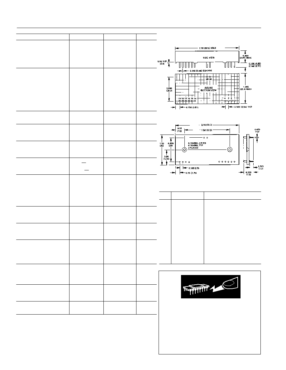
AD210 PIN DESIGNATIONS
Pin
Designation
Function
1
V
O
Output
2
O
COM
Output Common
3
+V
OSS
+Isolated Power @ Output
4
V
OSS
Isolated Power @ Output
14
+V
ISS
+Isolated Power @ Input
15
V
ISS
Isolated Power @ Input
16
FB
Input Feedback
17
IN
Input
18
I
COM
Input Common
19
+IN
+Input
29
Pwr Com
Power Common
30
Pwr
Power Input
AD210SPECIFICATIONS
(typical @ +25 C, and V
S
= +15 V unless otherwise noted)
Model
AD210AN
AD210BN
AD210JN
GAIN
Range
1 V/V 100 V/V
*
*
Error
±
2% max
±
1% max
*
vs. Temperature(0
°
C to +70
°
C)
+25 ppm/
°
C max
*
*
(25
°
C to +85
°
C)
±
50 ppm/
°
C max
*
*
vs. Supply Voltage
±
0.002%/V
*
*
Nonlinearity
1
±
0.025% max
±
0.012% max
*
INPUT VOLTAGE RATINGS
Linear Differential Range
±
10 V
*
*
Maximum Safe Differential Input
±
15 V
*
*
Max. CMV Input-to-Output
*
ac, 60 Hz, Continuous
2500 V rms
*
1500 V rms
dc, Continuous
±
3500 V peak
*
±
2000 V peak
Common-Mode Rejection
*
60 Hz, G = 100 V/V
*
R
S
500
Impedance Imbalance
120 dB
*
*
Leakage Current Input-to-Output
*
@ 240 V rms, 60 Hz
2
µ
A rms max
*
*
INPUT IMPEDANCE
Differential
l0
12
*
*
Common Mode
5 G
5 pF
*
*
INPUT BIAS CURRENT
Initial, @ +25
°
C
30 pA typ (400 pA max)
*
*
vs. Temperature (0
°
C to +70
°
C)
10 nA max
*
*
(25
°
C to +85
°
C)
30 nA max
*
*
INPUT DIFFERENCE CURRENT
Initial, @ +25
°
C
5 pA typ (200 pA max)
*
*
vs. Temperature(0
°
C to + 70
°
C)
2 nA max
*
*
(25
°
C to +85
°
C)
10 nA max
*
*
INPUT NOISE
Voltage (l kHz)
18 nV/
Hz
*
*
(10 Hz to 10 kHz)
4
µ
V rms
*
*
Current (1 kHz)
0.01 pA/
Hz
*
*
FREQUENCY RESPONSE
Bandwidth (3 dB)
*
G = 1 V/V
20 kHz
*
*
G = 100 V/V
15 kHz
*
*
Settling Time (
±
10 mV, 20 V Step)
*
G = 1 V/V
150
µ
s
*
*
G = 100 V/V
500
µ
s
*
*
Slew Rate (G = 1 V/V)
1 V/
µ
s
*
*
OFFSET VOLTAGE (RTI)
2
Initial, @ +25
°
C
±
15
±
45/G) mV max
(
±
5
±
15/G) mV max
*
vs. Temperature (0
°
C to +70
°
C)
(
±
10
±
30/G)
µ
V/
°
C
*
*
(25
°
C to +85
°
C)
(
±
10
±
50/G)
µ
V/
°
C
*
*
RATED OUTPUT
3
Voltage, 2 k
Load
±
10 V min
*
*
Impedance
1
max
*
*
Ripple (Bandwidth = 100 kHz)
10 mV p-p max
*
*
ISOLATED POWER OUTPUTS
4
Voltage, No Load
±
15 V
*
*
Accuracy
±
10%
*
*
Current
±
5 mA
*
*
Regulation, No Load to Full Load
See Text
*
*
Ripple
See Text
*
*
POWER SUPPLY
Voltage, Rated Performance
+15 V dc
±
5%
*
*
Voltage, Operating
+15 V dc
±
10%
*
*
Current, Quiescent
50 mA
*
*
Current, Full Load Full Signal
80 mA
*
*
TEMPERATURE RANGE
Rated Performance
25
°
C to +85
°
C
*
*
Operating
40
°
C to +85
°
C
*
*
Storage
40
°
C to +85
°
C
*
*
PACKAGE DIMENSIONS
Inches
1.00
×
2.10
×
0.350
*
*
Millimeters
25.4
×
53.3
×
8.9
*
*
NOTES
*Specifications same as AD210AN.
1
Nonlinearity is specified as a % deviation from a best straight line..
2
RTI Referred to Input.
3
A reduced signal swing is recommended when both
±
V
ISS
and
±
V
OSS
supplies are fully
loaded, due to supply voltage reduction.
4
See text for detailed information.
_
Specifications subject to change without notice.
REV. A
2
OUTLINE DIMENSIONS
Dimensions shown in inches and (mm).
AC1059 MATING SOCKET
CAUTION
ESD (electrostatic discharge) sensitive device. Elec-
trostatic charges as high as 4000 V readily accumu-
late on the human body and test equipment and can
discharge without detection. Although the AD210
features proprietary ESD protection circuitry, per-
manent damage may occur on devices subjected to
high energy electrostatic discharges. Therefore,
proper ESD precautions are recommended to avoid
performance degradation or loss of functionality.
WARNING!
ESD SENSITIVE DEVICE
AD210
REV. A
3
INSIDE THE AD210
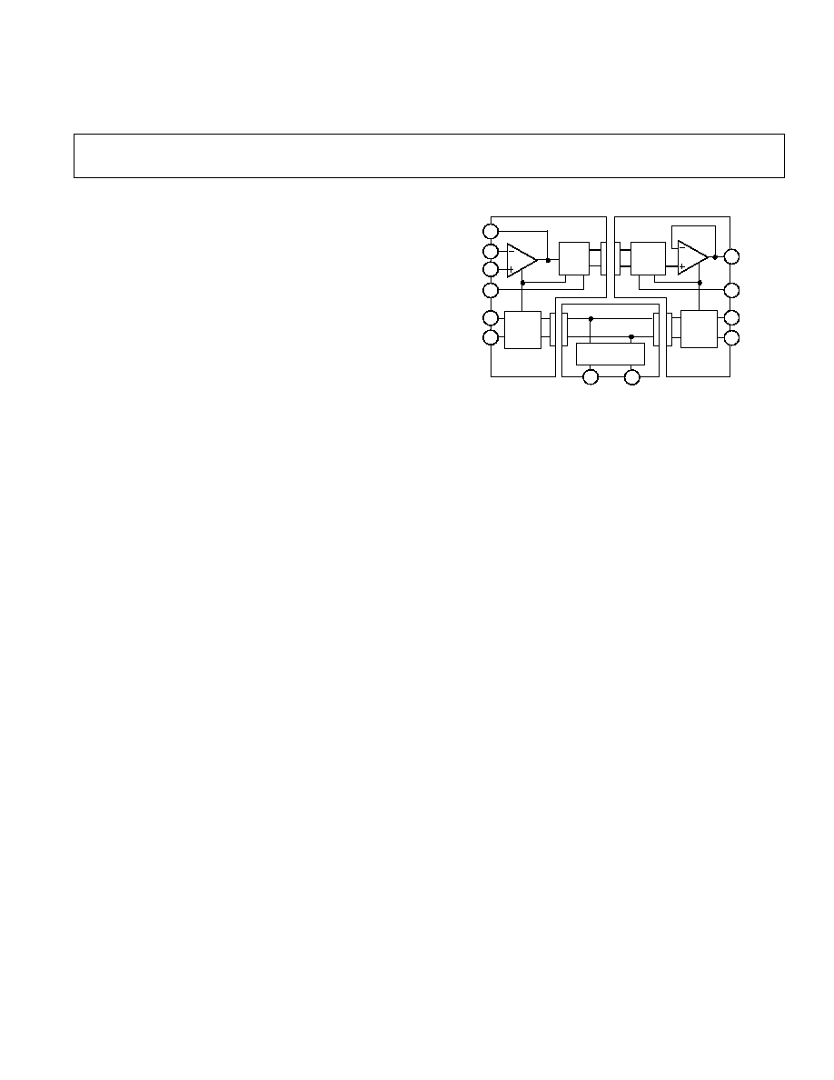
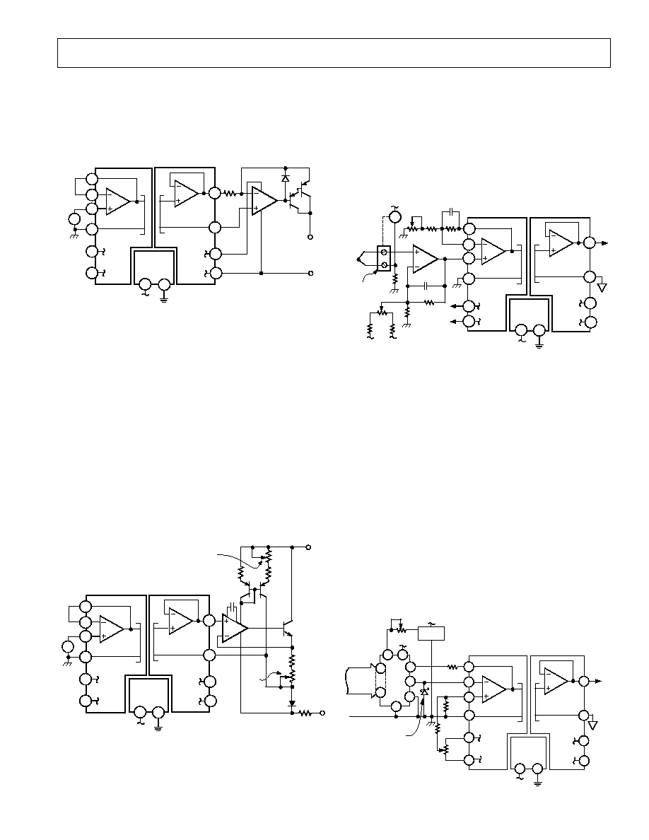
The AD210 basic block diagram is illustrated in Figure 1.
A +15 V supply is connected to the power port, and
±
15 V isolated power is supplied to both the input and
output ports via a 50 kHz carrier frequency. The uncom-
mitted input amplifier can be used to supply gain or buff-
ering of input signals to the AD210. The fullwave
modulator translates the signal to the carrier frequency for
application to transformer T1. The synchronous demodu-
lator in the output port reconstructs the input signal. A
20 kHz, three-pole filter is employed to minimize output
noise and ripple. Finally, an output buffer provides a low
impedance output capable of driving a 2 k
load.
INPUT
POWER
SUPPLY
19
14
15
16
17
18
V
O
30
29
T2
POWER
POWER
OSCILLATOR
INPUT
OUTPUT
MOD
DEMOD
FILTER
1
2
OUTPUT
POWER
SUPPLY
3
4
O
COM
+V
OSS
V
OSS
AD210
PWR COM
PWR
T3
T1
V
ISS
+V
ISS
I
COM
+IN
IN
FB
Figure 1. AD210 Block Diagram
USING THE AD210
The AD210 is very simple to apply in a wide range of ap-
plications. Powered by a single +15 V power supply, the
AD210 will provide outstanding performance when used
as an input or output isolator, in single and multichannel
configurations.
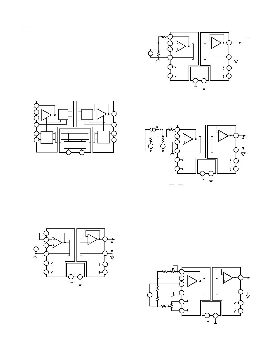
Input Configurations:
The basic unity gain configura-
tion for signals up to
±
10 V is shown in Figure 2. Addi-
tional input amplifier variations are shown in the following
figures. For smaller signal levels Figure 3 shows how to
obtain gain while maintaining a very high input impedance.
19
14
15
16
17
18
V
OUT
(
±
10V)
30
29
+V
OSS
V
SIG
±
10V
AD210
+V
ISS
V
ISS
+15V
2
3
4
V
OSS
1
V
OUT
Figure 2. Basic Unity Gain Configuration
The high input impedance of the circuits in Figures 2 and
3 can be maintained in an inverting application. Since the
AD210 is a three-port isolator, either the input leads or
the output leads may be interchanged to create the signal
inversion.
19
14
15
16
17
18
30
29
+V
OSS
V
SIG
AD210
+V
ISS
V
ISS
+15V
2
3
4
V
OSS
1
V
OUT
= V
SIG
1+
( )
R
F
R
G
R
G
R
F
Figure 3. Input Configuration for G > 1
Figure 4 shows how to accommodate current inputs or sum cur-
rents or voltages. This circuit configuration can also be used for
signals greater than
±
10 V. For example, a
±
100 V input span
can be handled with R
F
= 20 k
and R
S1
= 200 k
.
19
14
15
16
17
18
30
29
+V
OSS
AD210
+V
ISS
V
ISS
+15V
2
3
4
V
OSS
1
R
S1
I
S
V
S2
V
S1
R
S2
R
F
V
OUT
V
OUT
= R
F
V
S1
R
S1
( )
V
S2
R
S2
+
+ I
S
+ ...
Figure 4. Summing or Current Input Configuration
Adjustments
When gain and offset adjustments are required, the actual cir-
cuit adjustment components will depend on the choice of input
configuration and whether the adjustments are to be made at
the isolator's input or output. Adjustments on the output side
might be used when potentiometers on the input side would
represent a hazard due to the presence of high common-mode
voltage during adjustment. Offset adjustments are best done at
the input side, as it is better to null the offset ahead of the gain.
Figure 5 shows the input adjustment circuit for use when the in-
put amplifier is configured in the noninverting mode. This offset
adjustment circuit injects a small voltage in series with the
19
15
16
17
18
30
29
+V
OSS
AD210
+V
ISS
V
ISS
+15V
2
3
4
V
OSS
R
G
HI
V
OUT
V
SIG
14
200
47.5k
5k
100k
50k
LO
GAIN
OFFSET
1
Figure 5. Adjustments for Noninverting Input
AD210
REV. A
4
low side of the signal source. This will not work if the source has
another current path to input common or if current flows in the
signal source LO lead. To minimize CMR degradation, keep the
resistor in series with the input LO below a few hundred ohms.
Figure 5 also shows the preferred gain adjustment circuit. The
circuit shows R
F
of 50 k
, and will work for gains of ten or
greater. The adjustment becomes less effective at lower gains
(its effect is halved at G = 2) so that the pot will have to be a
larger fraction of the total R
F
at low gain. At G = 1 (follower)
the gain cannot be adjusted downward without compromising
input impedance; it is better to adjust gain at the signal source
or after the output.
Figure 6 shows the input adjustment circuit for use when the
input amplifier is configured in the inverting mode. The offset
adjustment nulls the voltage at the summing node. This is pref-
erable to current injection because it is less affected by subse-
quent gain adjustment. Gain adjustment is made in the feedback
and will work for gains from 1 V/V to 100 V/V.
19
15
16
17
18
30
29
+V
OSS
AD210
+V
ISS
V
ISS
+15V
2
3
4
V
OSS
V
OUT
V
SIG
14
200
47.5k
5k
100k
GAIN
OFFSET
50k
R
S
1
Figure 6. Adjustments for Inverting Input
Figure 7 shows how offset adjustments can be made at the out-
put, by offsetting the floating output port. In this circuit,
±
15 V
would be supplied by a separate source. The AD210's output
amplifier is fixed at unity, therefore, output gain must be made
in a subsequent stage.
19
15
16
17
18
30
29
+V
OSS
AD210
+V
ISS
V
ISS
+15V
2
3
4
V
OSS
V
OUT
14
200
1
0.1µF
100k
OFFSET
50k
+15V
15V
Figure 7. Output-Side Offset Adjustment
PCB
Layout for Multichannel Applications: The unique
pinout positioning minimizes board space constraints for multi-
channel applications. Figure 8 shows the recommended printed
circuit board layout for a noninverting input configuration with
gain.
R
F
R
G
R
F
R
G
R
F
R
G
POWER
CHANNEL INPUTS
1
2
3
0.1"
GRID
CHANNEL OUTPUTS
1
2
3
Figure 8. PCB Layout for Multichannel Applications with
Gain
Synchronization:
The AD210 is insensitive to the clock of an
adjacent unit, eliminating the need to synchronize the clocks.
However, in rare instances channel to channel pick-up may
occur if input signal wires are bundled together. If this happens,
shielded input cables are recommended.
PERFORMANCE CHARACTERISTICS
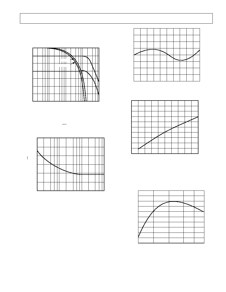
Common-Mode Rejection:
Figure 9 shows the common-
mode rejection of the AD210 versus frequency, gain and input
source resistance. For maximum common-mode rejection of
unwanted signals, keep the input source resistance low and care-
fully lay out the input, avoiding excessive stray capacitance at
the input terminals.
180
140
40
10 20 50 60 100 200 500 1k 2k 5k 10k
160
100
120
60
80
FREQUENCY Hz
R
LO
= 0
R
LO
= 500
R
LO
= 0
R
LO
= 10k
R
LO
= 10k
G = 100
G = 1
CMR dB
Figure 9. Common-Mode Rejection vs. Frequency
AD210
REV. A
5
+0.04
+0.03
+0.02
+0.01
0
0.01
0.02
0.03
0.04
10 8 6 4 2 0 +2 +4 +6 +8 +10
OUTPUT VOLTAGE SWING Volts
+8
+6
+4
+2
0
2
4
6
8
ERROR mV
ERROR %
Figure 12. Gain Nonlinearity Error vs. Output
0.01
0.009
0.008
0.007
0.006
0.005
0.004
0.003
0.002
0.001
0.000
100
90
80
70
60
50
40
30
20
10
0
0 2 4 6 8 10 12 14 16 18 20
TOTAL SIGNAL SWING Volts
ERROR % of Signal Swing
ERROR ppm of Signal Swing
Figure 13. Gain Nonlinearity vs. Output Swing
Gain vs. Temperature:
Figure 14 illustrates the AD210's
gain vs. temperature performance. The gain versus temperature
performance illustrated is for an AD210 configured as a unity
gain amplifier.
400
200
0
200
400
600
800
1000
1200
1400
1600
25 0 +25 +50 +70 +85
TEMPERATURE
°
C
GAIN ERROR ppm of Span
G = 1
Figure 14. Gain vs. Temperature
Phase Shift:
Figure 10 illustrates the AD210's low phase shift
and gain versus frequency. The AD210's phase shift and wide
bandwidth performance make it well suited for applications like
power monitors and controls systems.
60
20
80
100
100k
10k
1k
10
40
20
0
60
40
FREQUENCY Hz
0
20
40
60
80
100
120
140
PHASE SHIFT Degrees
GAIN dB
G = 1
G = 100
Figure 10. Phase Shift and Gain vs. Frequency
Input Noise vs. Frequency:
Voltage noise referred to the input
is dependent on gain and signal bandwidth. Figure 11 illustrates
the typical input noise in nV/
Hz
of the AD210 for a frequency
range from 10 to 10 kHz.
60
40
0
100
10k
1k
10
50
20
30
10
FREQUENCY Hz
NOISE nV/
Hz
Figure 11. Input Noise vs. Frequency
Gain Nonlinearity vs. Output:
Gain nonlinearity is defined as the
deviation of the output voltage from the best straight line, and is
specified as % peak-to-peak of output span. The AD210B provides
guaranteed maximum nonlinearity of
±
0.012% with an output span of
±
10 V. The AD210's nonlinearity performance is shown in Figure 12.
Gain Nonlinearity vs. Output Swing:
The gain nonlinearity
of the AD210 varies as a function of total signal swing. When
the output swing is less than 20 volts, the gain nonlinearity as a
fraction of signal swing improves. The shape of the nonlinearity
remains constant. Figure 13 shows the gain nonlinearity of the
AD210 as a function of total signal swing.
AD210
REV. A
6
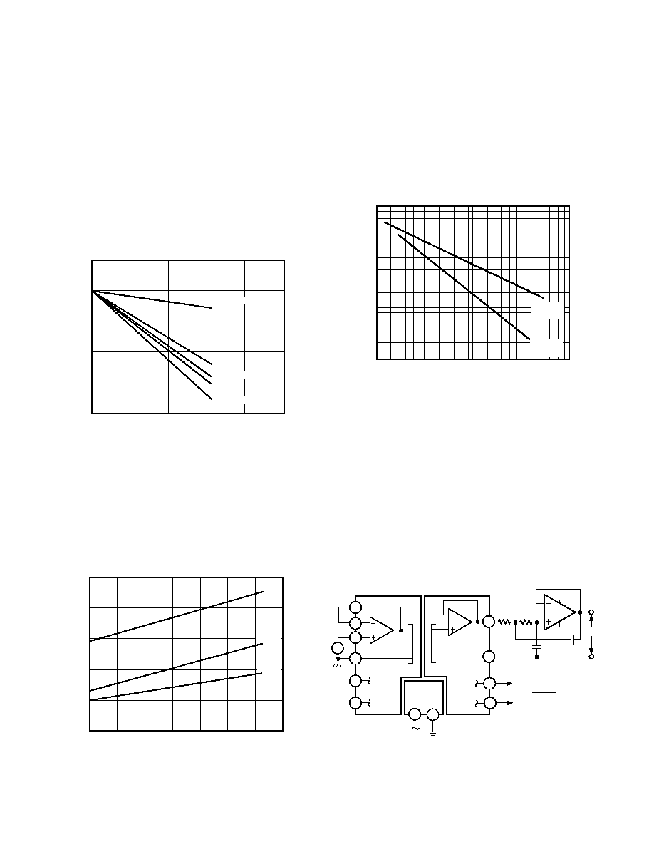
Isolated Power:
The AD210 provides isolated power at the
input and output ports. This power is useful for various signal
conditioning tasks. Both ports are rated at a nominal
±
15 V at
5 mA.
The load characteristics of the isolated power supplies are
shown in Figure 15. For example, when measuring the load
rejection of the input isolated supplies V
ISS
, the load is placed
between +V
ISS
and V
ISS
. The curves labeled V
ISS
and V
OSS
are
the individual load rejection characteristics of the input and the
output supplies, respectively.
There is also some effect on either isolated supply when loading
the other supply. The curve labeled CROSSLOAD indicates the
sensitivity of either the input or output supplies as a function of
the load on the opposite supply.
30
20
5
10
0
25
CURRENT mA
VOLTAGE
V
OSS
V
OSS
V
ISS
V
ISS
SIMULTANEOUS
SIMULTANEOUS
CROSSLOAD
30
Figure 15. Isolated Power Supplies vs. Load
Lastly, the curves labeled V
OSS
simultaneous and V
ISS
simulta-
neous indicate the load characteristics of the isolated power sup-
plies when an equal load is placed on both supplies.
The AD210 provides short circuit protection for its isolated
power supplies. When either the input supplies or the output
supplies are shorted to input common or output common,
respectively, no damage will be incurred, even under continuous
application of the short. However, the AD210 may be damaged
if the input and output supplies are shorted simultaneously.
100
50
1
0
75
LOAD mA
RIPPLE mV p-p
V
OSS
+V
ISS
30
25
0
+V
OSS
V
ISS
2
3
4
5
6
7
Figure 16a. Isolated Supply Ripple vs. Load
(External 4.7
µ
F Bypass)
Under any circumstances, care should be taken to ensure that
the power supplies do not accidentally become shorted.
The isolated power supplies exhibit some ripple which varies as
a function of load. Figure 16a shows this relationship. The
AD210 has internal bypass capacitance to reduce the ripple to a
point where performance is not affected, even under full load.
Since the internal circuitry is more sensitive to noise on the
negative supplies, these supplies have been filtered more heavily.
Should a specific application require more bypassing on the iso-
lated power supplies, there is no problem with adding external
capacitors. Figure 16b depicts supply ripple as a function of
external bypass capacitance under full load.
1V
10mV
0.1µF
100mV
1mV
CAPACITANCE
RIPPLE Peak-Peak Volts
1µF
10µF
100µF
( )
+V
ISS
+V
OSS
( )
V
ISS
V
OSS
Figure 16b. Isolated Power Supply Ripple vs. Bypass
Capacitance (Volts p-p, 1 MHz Bandwidth, 5 mA Load)
APPLICATIONS EXAMPLES
Noise Reduction in Data Acquisition Systems:
Transformer
coupled isolation amplifiers must have a carrier to pass both ac
and dc signals through their signal transformers. Therefore,
some carrier ripple is inevitably passed through to the isolator
output. As the bandwidth of the isolator is increased more of the
carrier signal will be present at the output. In most cases, the
ripple at the AD210's output will be insignificant when com-
pared to the measured signal. However, in some applications,
particularly when a fast analog-to-digital converter is used fol-
lowing the isolator, it may be desirable to add filtering; other-
wise ripple may cause inaccurate measurements. Figure 17
shows a circuit that will limit the isolator's bandwidth, thereby
reducing the carrier ripple.
V
OUT
15
30
29
+V
OSS
+V
ISS
V
ISS
+15V
2
4
V
OSS
14
1
0.001µF
0.002µF
R (k
) =
( )
112.5
f
C
(kHz)
AD542
+V
OSS
V
OSS
3
V
SIG
19
18
AD210
R
R
16
17
Figure 17. 2-Pole, Output Filter
Self-Powered Current Source
The output circuit shown in Figure 18 can be used to create a
self-powered output current source using the AD210. The 2 k
resistor converts the voltage output of the AD210 to an equiva-
AD210
REV. A
7
lent current V
OUT
/2 k
. This resistor directly affects the output
gain temperature coefficient, and must be of suitable stability for
the application. The external low power op amp, powered by
+V
OSS
and V
OSS,
maintains its summing junction at output
common. All the current flowing through the 2 k
resistor flows
through the output Darlington pass devices. A Darlington con-
figuration is used to minimize loss of output current to the base.
I
OUT
15
+V
OSS
+V
ISS
V
ISS
+15V
2
V
OSS
14
1
LF441
+V
OSS
V
OSS
3
V
SIG
0-10V
19
18
AD210
2k
2N3906
(2)
16
17
4
FDH333
I
OUT
RETURN
30
29
Figure 18. Self-Powered Isolated Current Source
The low leakage diode is used to protect the base-emitter junc-
tion against reverse bias voltages. Using V
OSS
as a current
return allows more than 10 V of compliance. Offset and gain
control may be done at the input of the AD210 or by varying
the 2 k
resistor and summing a small correction current
directly into the summing node. A nominal range of 1 mA
5 mA is recommended since the current output cannot reach
zero due to reverse bias and leakage currents. If the AD210 is
powered from the input potential, this circuit provides a fully
isolated, wide bandwidth current output. This configuration is
limited to 5 mA output current.
Isolated V-to-I Converter
Illustrated in Figure 19, the AD210 is used to convert a 0 V to
+10 V input signal to an isolated 420 mA output current. The
AD210 isolates the 0 V to +10 V input signal and provides a
proportional voltage at the isolator's output. The output circuit
converts the input voltage to a 420 mA output current, which
in turn is applied to the loop load R
LOAD
.
R
LOAD
15
+V
OSS
+V
ISS
V
ISS
+15V
2
V
OSS
14
1
+V
S
V
S
3
V
SIG
19
18
AD210
500
2N2907
16
17
4
CURRENT
LOOP
143
3.0k
ADJUST
TO 4mA
WITH 0V IN
+28V
CURRENT
LOOP
2N2219
576
1N4149
SPAN
ADJ
100
30
29
AD308
Figure 19. Isolated Voltage-to-Current Loop Converter
Isolated Thermocouple Amplifier
The AD210 application shown in Figure 20 provides amplifica-
tion, isolation and cold-junction compensation for a standard J
type thermocouple. The AD590 temperature sensor accurately
monitors the input terminal (cold-junction). Ambient tempera-
ture changes from 0
°
C to +40
°
C sensed by the AD590, are can-
celled out at the cold junction. Total circuit gain equals 183;
100 and 1.83, from A1 and the AD210 respectively. Calibration
is performed by replacing the thermocouple junction with plain
thermocouple wire and a millivolt source set at 0.0000 V (0
°
C)
and adjusting R
O
for E
OUT
equal to 0.000 V. Set the millivolt
source to +0.02185 V (400
°
C) and adjust R
G
for V
OUT
equal to
+4.000 V. This application circuit will produce a nonlinearized
output of about +10 mV/
°
C for a 0
°
C to +400
°
C range.
+V
OSS
+V
ISS
V
ISS
+15V
2
V
OSS
3
18
AD210
16
17
4
13.7k
30
29
10k
R
G
5k
A1
19
V
ISS
10k
220pF
100k
THERMAL
CONTACT
52.3
COLD
JUNCTION
V
ISS
+V
ISS
1k
-20k-
"J"
15
14
1000pF
1
V
OUT
AD590
AD OP-07
R
G
Figure 20. Isolated Thermocouple Amplifier
Precision Floating Programmable Reference
The AD210, when combined with a digital-to-analog converter,
can be used to create a fully floating voltage output. Figure 21
shows one possible implementation.
The digital inputs of the AD7541 are TTL or CMOS compat-
ible. Both the AD7541 and AD581 voltage reference are pow-
ered by the isolated power supply + V
ISS
. I
COM
should be tied to
input digital common to provide a digital ground reference for
the inputs.
The AD7541 is a current output DAC and, as such, requires an
external output amplifier. The uncommitted input amplifier
internal to the AD210 may be used for this purpose. For best
results, its input offset voltage must be trimmed as shown.
The output voltage of the AD210 will go from 0 V to 10 V for
digital inputs of 0 and full scale, respectively. However, since
the output port is truly isolated, V
OUT
and O
COM
may be freely
interchanged to get 0 V to +10 V.
This circuit provides a precision 0 V10 V programmable refer-
ence with a
±
3500 V common-mode range.
+V
OSS
+V
ISS
V
ISS
+15V
V
OSS
AD210
200
1k
+V
ISS
V
OUT
0 - 10V
100k
50k
17
1
3
2
18
16
12-BIT
DIGITAL
INPUT
AD7541
2k
GAIN
HP5082-2811
OR EQUIVALENT
+V
ISS
AD581
OFFSET
17
15
4
1
3
2
18
16
4
15
19
14
30
29
Figure 21. Precision Floating Programmable Reference
AD210
REV. A
8
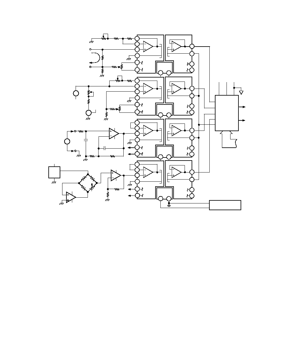
MULTICHANNEL DATA ACQUISITION FRONT-END
Illustrated in Figure 22 is a four-channel data acquisition front-
end used to condition and isolate several common input signals
found in various process applications. In this application, each
AD210 will provide complete isolation from input to output as
well as channel to channel. By using an isolator per channel,
maximum protection and rejection of unwanted signals is
obtained. The three-port design allows the AD210 to be
configured as an input or output isolator. In this application the
isolators are configured as input devices with the power port
providing additional protection from possible power source
faults.
Channel 1:
The AD210 is used to convert a 420 mA current
loop input signal into a 0 V10 V input. The 25
shunt resistor
converts the 4-20 mA current into a +100 mV to +500 mV signal.
The signal is offset by 100 mV via R
O
to produce a 0 mV to
+400 mV input. This signal is amplified by a gain of 25 to produce
the desired 0 V to +10 V output. With an open circuit, the AD210
will show 2.5 V at the output.
Channel 2:
In this channel, the AD210 is used to condition and
isolate a current output temperature transducer, Model AD590. At
+25
°
C, the AD590 produces a nominal current of 298.2
µ
A. This
level of current will change at a rate of 1
µ
A/
°
C. At 17.8
°
C (0
°
F),
the AD590 current will be reduced by 42.8
µ
A to +255.4
µ
A. The
AD580 reference circuit provides an equal but opposite current,
resulting in a zero net current flow, producing a 0 V output from
the AD210. At +100
°
C (+212
°
F), the AD590 current output will
be 373.2
µ
A minus the 255.4
µ
A offsetting current from the
AD580 circuit to yield a +117.8
µ
A input current. This current is
converted to a voltage via R
F
and R
G
to produce an output of
+2.12 V. Channel 2 will produce an output of +10 mV/
°
F over a
0
°
F to +212
°
F span.
Channel 3:
Channel 3 is a low level input channel configured with
a high gain amplifier used to condition millivolt signals. With the
AD210's input set to unity and the input amplifier set for a gain of
1000, a
±
10 mV input will produce a
±
10 V at the AD210's output.
Channel 4:
Channel 4 illustrates one possible configuration for
conditioning a bridge circuit. The AD584 produces a +10 V
excitation voltage, while A1 inverts the voltage, producing negative
excitation. A2 provides a gain of 1000 V/V to amplify the low level
bridge signal. Additional gain can be obtained by reconfiguration
of the AD210's input amplifier.
±
V
ISS
provides the complete power
for this circuit, eliminating the need for a separate isolated excita-
tion source.
Each channel is individually addressed by the multiplexer's chan-
nel select. Additional filtering or signal conditioning should follow
the multiplexer, prior to an analog-to-digital conversion stage.
+V
OSS
+V
ISS
V
ISS
V
OSS
AD210
R
O
50k
17
15
18
16
19
14
4
3
29
COM
+V
TO A/D
+V
OSS
+V
ISS
V
ISS
V
OSS
OFFSET
50k
17
15
18
16
19
14
4
3
2
30
29
+V
ISS
V
ISS
15
+V
OSS
V
OSS
AD210
18
19
14
4
3
2
1
30
+V
OSS
V
OSS
AD210
17
18
16
19
4
3
1
30
29
R
G
1k
1
200k
8.25k
AD210
1
10T
4-20mA
25
50k
1k
R
G
5k
10T
R
F
15.8k
10T
50k
30
16
17
100
AD590
AD580
V
ISS
+V
ISS
R
O
1k
10T
9.31k
AD OP-07
+V
ISS
V
ISS
+V
ISS
V
ISS
15
14
0.47µF
50k
50
1.0µF
39k
E
IN
1M
1k
20k
20k
20k
20k
+V
ISS
V
ISS
29
+V
ISS
V
ISS
A2
A1
AD584
+V
ISS
COM
+15V
DC POWER
SOURCE
2
2
AD7502
MULTIPLEXER
V
CHANNEL
SELECT
CHANNEL 3
CHANNEL 1
CHANNEL 2
CHANNEL 4
+10V
A1; A2 = AD547
Figure 22. Multichannel Data Acquisition Front-End
C100599/86
PRINTED IN U.S.A.