REV. B
Information furnished by Analog Devices is believed to be accurate and
reliable. However, no responsibility is assumed by Analog Devices for its
use, nor for any infringements of patents or other rights of third parties that
may result from its use. No license is granted by implication or otherwise
under any patent or patent rights of Analog Devices.
a
AD5200/AD5201
One Technology Way, P.O. Box 9106, Norwood, MA 02062-9106, U.S.A.
Tel: 781/329-4700
www.analog.com
Fax: 781/326-8703
© Analog Devices, Inc., 2001
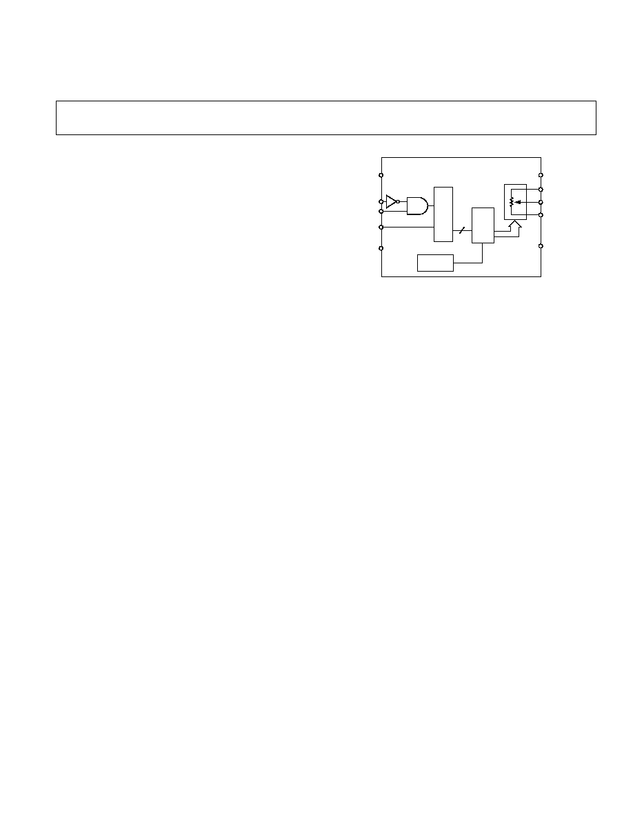
FUNCTIONAL BLOCK DIAGRAM
SER
REG
PWR-ON
PRESET
A
W
B
RDAC
REG
Dx
8/6
CS
CLK
SDI
AD5200/AD5201
V
SS
V
DD
GND
SHDN
256-Position and 33-Position
Digital Potentiometers
FEATURES
AD5200--256-Position
AD5201--33-Position
10 k , 50 k
3-Wire SPI-Compatible Serial Data Input
Single Supply 2.7 V to 5.5 V or
Dual Supply 2.7 V for AC or Bipolar Operations
Internal Power-On Midscale Preset
APPLICATIONS
Mechanical Potentiometer Replacement
Instrumentation: Gain, Offset Adjustment
Programmable Voltage-to-Current Conversion
Programmable Filters, Delays, Time Constants
Line Impedance Matching
GENERAL DESCRIPTION
The AD5200 and AD5201 are programmable resistor devices,
with 256 positions and 33 positions respectively, that can be digi-
tally controlled through a 3-wire SPI serial interface. The terms
programmable resistor, variable resistor (VR), and RDAC are
commonly used interchangeably to refer to digital potentiometers.
These devices perform the same electronic adjustment function
as a potentiometer or variable resistor. Both AD5200/AD5201
contain a single variable resistor in the compact
µSOIC-10
package. Each device contains a fixed wiper resistance at the
wiper contact that taps the programmable resistance at a point
determined by a digital code. The code is loaded in the serial
input register. The resistance between the wiper and either end
point of the programmable resistor varies linearly with respect to
the digital code transferred into the VR latch. Each variable
resistor offers a completely programmable value of resistance,
between the A terminal and the wiper, or the B terminal and the
wiper. The fixed A-to-B terminal resistance of 10 k
or 50 k
has a nominal temperature coefficient of 500 ppm/
∞C. The VR
has a VR latch that holds its programmed resistance value. The
VR latch is updated from an SPI-compatible serial-to-parallel
shift register that is loaded from a standard 3-wire serial-input
digital interface. Eight data bits for the AD5200 and six data
bits for the AD5201 make up the data word that is clocked into
the serial input register. The internal preset forces the wiper to
the midscale position by loading 80
H
and 10
H
into AD5200 and
AD5201 VR latches respectively. The
SHDN pin forces the
resistor to an end-to-end open-circuit condition on the A terminal
and shorts the wiper to the B terminal, achieving a microwatt
power shutdown state. When
SHDN is returned to logic high,
the previous latch setting puts the wiper in the same resistance
setting prior to shutdown. The digital interface is still active dur-
ing shutdown so that code changes can be made that will produce
a new wiper position when the device is returned from shutdown.
All parts are guaranteed to operate over the extended industrial
temperature range of ≠40
∞C to +85∞C.

REV. B
≠2≠
AD5200/AD5201≠SPECIFICATIONS
AD5200 ELECTRICAL CHARACTERISTICS
Parameter
Symbol
Conditions
Min
Typ
1
Max
Unit
DC CHARACTERISTICS RHEOSTAT MODE
Resistor Differential Nonlinearity
2
R-DNL
R
WB
, V
A
= No Connect
≠1
± 0.25 +1
LSB
Resistor Integral Nonlinearity
2
R-INL
R
WB
, V
A
= No Connect
≠2
± 0.5 +2
LSB
Nominal Resistor Tolerance
3
R
AB
T
A
= 25
∞C
≠30
+30
%
Resistance Temperature Coefficient
R
AB
/
T
V
AB
= V
DD
, Wiper = No Connect
500
ppm/
∞C
Wiper Resistance
R
W
V
DD
= 5 V
50
100
DC CHARACTERISTICS POTENTIOMETER DIVIDER MODE (Specifications apply to all VRs.)
Resolution
N
8
Bits
Differential Nonlinearity
4
DNL
≠1
± 1/4 +1
LSB
Integral Nonlinearity
4
INL
≠2
± 1/2 +2
LSB
Voltage Divider Temperature Coefficient
V
W
/
T
Code = 80
H
5
ppm/
∞C
Full-Scale Error
V
WFSE
Code = FF
H
≠1.5
≠0.5
0
LSB
Zero-Scale Error
V
WZSE
Code = 00
H
0
+0.5
+1.5
LSB
RESISTOR TERMINALS
Voltage Range
5
V
A,
B,
W
V
SS
V
DD
V
Capacitance
6
A, B
C
A,
B
f = 1 MHz, Measured to GND, Code = 80
H
45
pF
Capacitance
6
W
C
W
f = 1 MHz, Measured to GND, Code = 80
H
60
pF
Shutdown Supply Current
7
I
DD_SD
V
DD
= 5.5 V
0.01
5
µA
Common-Mode Leakage
I
CM
V
A
= V
B
= V
DD
/2
1
nA
DIGITAL INPUTS AND OUTPUTS
Input Logic High
V
IH
2.4
V
Input Logic Low
V
IL
0.8
V
Input Logic High
V
IH
V
DD
= 3 V, V
SS
= 0 V
2.1
V
Input Logic Low
V
IL
V
DD
= 3 V, V
SS
= 0 V
0.6
V
Input Current
I
IL
V
IN
= 0 V or 5 V
±1
µA
Input Capacitance
6
C
IL
5
pF
POWER SUPPLIES
Logic Supply
V
LOGIC
2.7
5.5
V
Power Single-Supply Range
V
DD
RANGE
V
SS
= 0 V
≠0.3
5.5
V
Power Dual-Supply Range
V
DD/SS
RANGE
± 2.3
± 2.7
V
Positive Supply Current
I
DD
V
IH
= +5 V or V
IL
= 0 V
15
40
µA
Negative Supply Current
I
SS
V
SS
= ≠5 V
15
40
µA
Power Dissipation
8
P
DISS
V
IH
= +5 V or V
IL
= 0 V, V
DD
= +5 V, V
SS
= 0 V
0.2
mW
Power Supply Sensitivity
PSS
V
DD
= +5 V
± 10%, Code = Midscale
≠0.01 0.001 +0.01
%/%
DYNAMIC CHARACTERISTICS
6, 9
Bandwidth ≠3 dB
BW_10 k
R
AB
= 10 k
, Code = 80
H
600
kHz
BW_50 k
R
AB
= 50 k
, Code = 80
H
100
kHz
Total Harmonic Distortion
THD
W
V
A
= 1 V rms, V
B
= 0 V, f = 1 kHz, R
AB
= 10 k
0.003
%
V
W
Settling Time (10 k
/50 k)
t
S
V
A
= 5 V, V
B
= 0 V,
± 1 LSB Error Band
2/9
µs
Resistor Noise Voltage Density
e
N_WB
R
WB
= 5 k
, RS = 0
9
nV
Hz
NOTES
1
Typicals represent average readings at 25
∞C and V
DD
= 5 V, V
SS
= 0 V.
2
Resistor position nonlinearity error R-INL is the deviation from an ideal value measured between the maximum resistance and the minimum resistance wiper posi-
tions. R-DNL measures the relative step change from ideal between successive tap positions. Parts are guaranteed monotonic. I
W
= V
DD
/R for both V
DD
= +2.7 V,
V
SS
= ≠2.7 V.
3
V
AB
= V
DD
, Wiper (V
W
) = No connect.
4
INL and DNL are measured at V
W
with the RDAC configured as a potentiometer divider similar to a voltage output D/A converter. V
A
= V
DD
and V
B
= 0 V. DNL
specification limits of
± 1 LSB maximum are Guaranteed Monotonic operating conditions.
5
Resistor Terminals A, B, W have no limitations on polarity with respect to each other.
6
Guaranteed by design and not subject to production test.
7
Measured at the A terminal. A terminal is open-circuited in shutdown mode.
8
P
DISS
is calculated from (I
DD
◊ V
DD
). CMOS logic level inputs result in minimum power dissipation.
9
All dynamic characteristics use V
DD
= 5 V, V
SS
= 0 V.
Specifications subject to change without notice.
(V
DD
= 5 V
10%, or 3 V 10%, V
SS
= 0 V, V
A
= +V
DD
, V
B
= 0 V,
≠40 C < T
A
< +85 C unless otherwise noted.)

REV. B
≠3≠
AD5200/AD5201
(V
DD
= 5 V 10%, or 3 V 10%, V
SS
= 0 V, V
A
= +V
DD
, V
B
= 0 V,
≠40 C < T
A
< +85 C unless otherwise noted.)
AD5201 ELECTRICAL CHARACTERISTICS
Parameter
Symbol
Conditions
Min
Typ
1
Max
Unit
DC CHARACTERISTICS RHEOSTAT MODE
Resistor Differential Nonlinearity
2
R-DNL
R
WB
, V
A
= No Connect
≠0.5
± 0.05 +0.5
LSB
Resistor Integral Nonlinearity
2
R-INL
R
WB
, V
A
= No Connect
≠1
± 0.1 +1
LSB
Nominal Resistor Tolerance
3
R
AB
T
A
= 25
∞C
≠30
+30
%
Resistance Temperature Coefficient
R
AB
/
T
V
AB
= V
DD
, Wiper = No Connect
500
ppm/
∞C
Wiper Resistance
R
W
V
DD
= 5 V
50
100
DC CHARACTERISTICS POTENTIOMETER DIVIDER MODE (Specifications apply to all VRs.)
Resolution
4
N
6
Bits
Differential Nonlinearity
5
DNL
≠0.5
± 0.01 +0.5
LSB
Integral Nonlinearity
5
INL
≠1
± 0.02 +1
LSB
Voltage Divider Temperature Coefficient
V
W
/
T
Code = 10
H
5
ppm/
∞C
Full-Scale Error
V
WFSE
Code = 20
H
≠1/2
≠1/4
0
LSB
Zero-Scale Error
V
WZSE
Code = 00
H
0
+1/4
+1/2
LSB
RESISTOR TERMINALS
Voltage Range
6
V
A,
B,
W
V
SS
V
DD
V
Capacitance
7
A, B
C
A,
B
f = 1 MHz, Measured to GND, Code = 10
H
45
pF
Capacitance
7
W
C
W
f = 1 MHz, Measured to GND, Code = 10
H
60
pF
Shutdown Supply Current
8
I
DD_SD
V
DD
= 5.5 V
0.01
5
µA
Common-Mode Leakage
I
CM
V
A
= V
B
= V
DD
/2
1
nA
DIGITAL INPUTS AND OUTPUTS
Input Logic High
V
IH
2.4
V
Input Logic Low
V
IL
0.8
V
Input Logic High
V
IH
V
DD
= 3 V, V
SS
= 0 V
2.1
V
Input Logic Low
V
IL
V
DD
= 3 V, V
SS
= 0 V
0.6
V
Input Current
I
IL
V
IN
= 0 V or 5 V
±1
µA
Input Capacitance
7
C
IL
5
pF
POWER SUPPLIES
Logic Supply
V
LOGIC
2.7
5.5
V
Power Single-Supply Range
V
DD
RANGE
V
SS
= 0 V
≠0.3
5.5
V
Power Dual-Supply Range
V
DD/SS
RANGE
± 2.3
± 2.7
V
Positive Supply Current
I
DD
V
IH
= +5 V or V
IL
= 0 V
15
40
µA
Negative Supply Current
I
SS
V
SS
= ≠5 V
15
40
µA
Power Dissipation
9
P
DISS
V
IH
= +5 V or V
IL
= 0 V, V
DD
= +5 V, V
SS
= ≠5 V
0.2
mW
Power Supply Sensitivity
PSS
V
DD
= +5 V
± 10%
≠0.01 0.001 +0.01
%/%
DYNAMIC CHARACTERISTICS
7, 10
Bandwidth ≠3 dB
BW_10 k
R
AB
= 10 k
, Code = 10
H
600
kHz
BW_50 k
R
AB
= 50 k
, Code = 10
H
100
kHz
Total Harmonic Distortion
THD
W
V
A
= 1 V rms, V
B
= 0 V, f = 1 kHz, R
AB
= 10 k
0.003
%
V
W
Settling Time (10 k
/50 k)
t
S
V
A
= 5 V, V
B
= 0 V,
± 1 LSB Error Band
2/9
µs
Resistor Noise Voltage Density
e
N_WB
R
WB
= 5 k
, RS = 0
9
nV
Hz
NOTES
1
Typicals represent average readings at 25
∞C and V
DD
= 5 V, V
SS
= 0 V.
2
Resistor position nonlinearity error R-INL is the deviation from an ideal value measured between the maximum resistance and the minimum resistance wiper posi-
tions. R-DNL measures the relative step change from ideal between successive tap positions. Parts are guaranteed monotonic. I
W
= V
DD
/R for both V
DD
= +2.7 V,
V
SS
= ≠2.7 V.
3
V
AB
= V
DD
, Wiper (V
W
) = No connect.
4
Six bits are needed for 33 positions even though it is not a 64-position device.
5
INL and DNL are measured at V
W
with the RDAC configured as a potentiometer divider similar to a voltage output D/A converter. V
A
= V
DD
and V
B
= 0 V. DNL
specification limits of
±1 LSB maximum are Guaranteed Monotonic operating conditions.
6
Resistor Terminals A, B, W have no limitations on polarity with respect to each other.
7
Guaranteed by design and not subject to production test.
8
Measured at the A terminal. A terminal is open-circuited in shutdown mode.
9
P
DISS
is calculated from (I
DD
◊ V
DD
). CMOS logic level inputs result in minimum power dissipation.
10
All dynamic characteristics use V
DD
= 5 V, V
SS
= 0 V.
Specifications subject to change without notice.
REV. B
≠4≠
AD5200/AD5201≠SPECIFICATIONS
ELECTRICAL CHARACTERISTICS
Parameter
Symbol
Conditions
Min
Typ
1
Max
Unit
INTERFACE TIMING CHARACTERISTICS (Applies to All Parts [Notes 2, 3])
Input Clock Pulsewidth
t
CH
, t
CL
Clock Level High or Low
20
ns
Data Setup Time
t
DS
5
ns
Data Hold Time
t
DH
5
ns
CS Setup Time
t
CSS
15
ns
CS High Pulsewidth
t
CSW
40
ns
CLK Fall to
CS Fall Hold Time
t
CSH0
0
ns
CLK Fall to
CS Rise Hold Time
t
CSH1
0
ns
CS Rise to Clock Rise Setup
t
CS1
10
ns
NOTES
1
Typicals represent average readings at 25
∞C and V
DD
= 5 V, V
SS
= 0 V.
2
Guaranteed by design and not subject to production test.
3
See timing diagram for location of measured values. All input control voltages are specified with t
R
= t
F
= 2 ns (10% to 90% of 3 V) and timed from a voltage level of
1.5 V. Switching characteristics are measured using V
LOGIC
= 5 V.
Specifications subject to change without notice.
(V
DD
= 5 V 10%, or 3 V 10%, V
SS
= 0 V, V
A
= +V
DD
, V
B
= 0 V, ≠40 C < T
A
< +85 C
unless otherwise noted.)
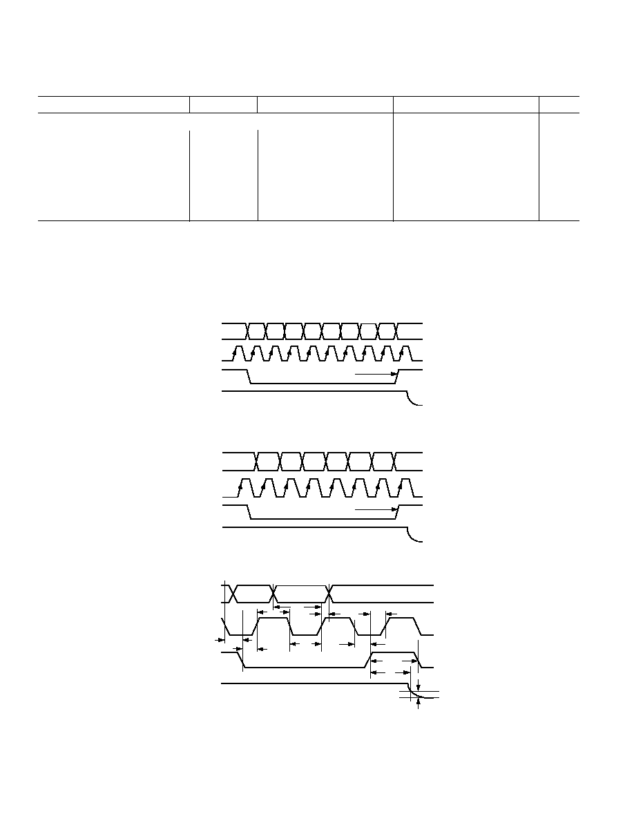
D7
D6
D5
D4
D3
D2
D1
D0
0
1
SDI
0
1
CLK
0
1
VOUT
0
1
CS
DAC REGISTER LOAD
Figure 1a. AD5200 Timing Diagram
0
1
SDI
D5
D4
D3
D2
D1
D0
0
1
CLK
0
1
CS
DAC REGISTER LOAD
0
1
VOUT
Figure 1b. AD5201 Timing Diagram
Dx
Dx
0
1
0
1
0
1
0
V
DD
SDI
(DATA IN)
CLK
CS
VOUT
t
CH
t
DS
t
DH
t
CS1
t
CSW
t
S
t
CL
t
CSH0
t
CSS
1LSB
t
CSH1
Figure 1c. Detail Timing Diagram

REV. B
AD5200/AD5201
≠5≠
ABSOLUTE MAXIMUM RATINGS
1
(T
A
= 25
∞C, unless otherwise noted)
V
DD
to V
SS
. . . . . . . . . . . . . . . . . . . . . . . . . . . . . . . . . . . . . 7 V
V
DD
to GND . . . . . . . . . . . . . . . . . . . . . . . . . . . . . ≠0.3, +7 V
V
SS
to GND . . . . . . . . . . . . . . . . . . . . . . . . . . . . . . . 0 V, ≠7 V
V
A
, V
B
, V
W
to GND . . . . . . . . . . . . . . . . . . . . . . . . . V
SS
, V
DD
I
MAX
. . . . . . . . . . . . . . . . . . . . . . . . . . . . . . . . . . . . .
±20 mA
2
Digital Inputs and Output Voltage to GND . . . . . . . 0 V, 7 V
Operating Temperature Range . . . . . . . . . . . ≠40
∞C to +85∞C
Maximum Junction Temperature (T
J
Max) . . . . . . . . . 150
∞C
Storage Temperature . . . . . . . . . . . . . . . . . . ≠65
∞C to +150∞C
Lead Temperature (Soldering, 10 sec) . . . . . . . . . . . . 300
∞C
Thermal Resistance
JA,
µSOIC-10 . . . . . . . . . . . . . 200∞C/W
Package Power Dissipation = (T
J
Max ≠ T
A
)/
JA
NOTES
1
Stresses above those listed under Absolute Maximum Ratings may cause perma-
nent damage to the device. This is a stress rating; functional operation of the device
at these or any other conditions above those listed in the operational sections of this
specification is not implied. Exposure to absolute maximum rating conditions for
extended periods may affect device reliability.
2
Max current is bounded by the maximum current handling of the switches,
maximum power dissipation of the package, and maximum applied voltage across
any two of the A, B, and W terminals at a given resistance. Please refer to TPC 31
and TPC 32 for detail.
PIN CONFIGURATION
TOP VIEW
(Not to Scale)
10
9
8
7
6
1
2
3
4
5
AD5200/
AD5201
B
V
SS
GND
CS
SDI
A
W
V
DD
SHDN
CLK
CAUTION
ESD (electrostatic discharge) sensitive device. Electrostatic charges as high as 4000 V readily
accumulate on the human body and test equipment and can discharge without detection. Although
the AD5200/AD5201 features proprietary ESD protection circuitry, permanent damage may occur
on devices subjected to high-energy electrostatic discharges. Therefore, proper ESD precautions
are recommended to avoid performance degradation or loss of functionality.
WARNING!
ESD SENSITIVE DEVICE
PIN FUNCTION DESCRIPTIONS
Pin
Name
Description
1
B
B Terminal.
2
V
SS
Negative Power Supply, specified for opera-
tion from 0 V to ≠2.7 V.
3
GND
Ground.
4
CS
Chip Select Input, Active Low. When
CS
returns high, data will be loaded into the
DAC register.
5
SDI
Serial Data Input.
6
CLK
Serial Clock Input, positive edge triggered.
7
SHDN
Active Low Input. Terminal A open circuit.
Shutdown controls Variable Resistors of
RDAC to temporary infinite.
8
V
DD
Positive Power Supply (Sum of V
DD
+ V
SS
5.5 V).
9
W
Wiper Terminal.
10
A
A Terminal.
ORDERING GUIDE
Temperature
Package
Package
Full
Branding
Model
RES
k
Range
Description
Option
Reel Qty.
Information
AD5200BRM10-REEL7
256
10
≠40
∞C/+85∞C
µSOIC-10
RM-10
5000
DLA
AD5200BRM50-REEL7
256
50
≠40
∞C/+85∞C
µSOIC-10
RM-10
5000
DLB
AD5201BRM10-REEL7
33
10
≠40
∞C/+85∞C
µSOIC-10
RM-10
5000
DMA
AD5201BRM50-REEL7
33
50
≠40
∞C/+85∞C
µSOIC-10
RM-10
5000
DMB

REV. B
≠6≠
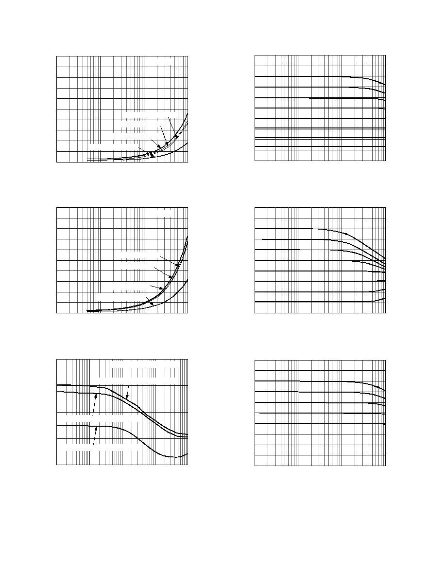
AD5200/AD5201≠Typical Performance Characteristics
CODE ≠ Decimal
0.20
RDNL ≠ LSB
224
0.15
0.10
0.05
0.00
0.05
0.10
0.15
0.20
192
160
128
96
64
32
0
256
V
DD
= 2.7V, V
SS
= 0V
V
DD
= 5.5V, V
SS
= 0V
V
DD
= +2.7V, V
SS
= ≠2.7V
TPC 1. AD5200 10 k
RDNL vs. Code
CODE ≠ Decimal
RDNL
≠
LSB
28
≠0.02
≠0.01
0.00
0.01
0.02
0.03
24
20
16
12
8
4
0
32
≠0.03
V
DD
= 2.7V, V
SS
= 0V
V
DD
= 5.5V, V
SS
= 0V
V
DD
= +2.7V, V
SS
= ≠2.7V
TPC 2. AD5201 10 k
RDNL vs. Code
CODE ≠ Decimal
RINL
≠
LSB
224
0.0
0.1
0.2
0.3
0.5
0.7
192
160
128
96
64
32
0
256
≠0.1
V
DD
= 2.7V, V
SS
= 0V
V
DD
= 5.5V, V
SS
= 0V
V
DD
= +2.7V, V
SS
= ≠2.7V
0.6
0.4
TPC 3. AD5200 10 k
RINL vs. Code
CODE ≠ Decimal
RINL
≠
LSB
28
0.00
0.02
0.04
0.06
0.08
0.12
24
20
16
12
8
4
0
32
≠0.02
V
DD
= +2.7V
V
SS
= ≠2.7V
V
DD
= 2.7V, V
SS
= 0V
V
DD
= 5.5V, V
SS
= 0V
0.10
TPC 4. AD5201 10 k
RINL vs. Code
CODE ≠ Decimal
DNL
≠
LSB
224
≠0.25
≠0.20
≠0.15
≠0.10
≠0.05
0.10
192
160
128
96
64
32
0
256
≠0.30
V
DD
= +2.7V, V
SS
= ≠2.7V
V
DD
= 5.5V, V
SS
= 0V
V
DD
= 2.7V, V
SS
= 0V
0.00
0.05
TPC 5. AD5200 10 k
DNL vs. Code
CODE ≠ Decimal
DNL
≠
LSB
28
≠0.005
0.000
0.005
0.010
0.020
24
20
16
12
8
4
0
32
≠0.010
V
DD
= +2.7V, V
SS
= ≠2.7V
V
DD
= 5.5V, V
SS
= 0V
V
DD
= 2.7V, V
SS
= 0V
0.015
TPC 6. AD5201 10 k
DNL vs. Code

REV. B
AD5200/AD5201
≠7≠
CODE ≠ Decimal
INL
≠
LSB
224
≠0.2
≠0.1
0.0
0.1
0.3
192
160
128
96
64
32
0
256
≠0.3
V
DD
= +2.7V, V
SS
= ≠2.7V
V
DD
= 5.5V, V
SS
= 0V
V
DD
= 2.7V, V
SS
= 0V
0.2
≠0.4
≠0.5
TPC 7. AD5200 10 k
INL vs. Code
CODE ≠ Decimal
INL
≠
LSB
28
0.005
0.010
0.020
24
20
16
12
8
4
0
32
0.000
V
DD
= +2.7V, V
SS
= ≠2.7V
V
DD
= 5.5V, V
SS
= 0V
V
DD
= 2.7V, V
SS
= 0V
0.015
≠0.005
≠0.010
TPC 8. AD5201 10 k
INL vs. Code
V
IH
≠ V
I
DD
/I
SS
≠
mA
0.01
0.1
10
5.0
4.0
3.0
2.0
1.0
0.0
0.001
1.0
I
DD
@ V
DD
/V
SS
= 5V/0V
I
DD
@ V
DD
/V
SS
= 3V/0V
I
DD
@ V
DD
/V
SS
= 2.5V
I
SS
@ V
DD
/V
SS
= 2.5V
TPC 9. Supply Current vs. Logic Input Voltage
TEMPERATURE ≠ C
I
DD
SUPPLY CURRENT
≠
A
20
≠40
18
16
14
12
10
8
6
4
2
0
≠20
0
20
40
60
80
100
V
IL
= V
SS
V
IH
= V
DD
V
DD
= 5.5V
V
DD
= 2.7V
TPC 10. Supply Current vs. Temperature
TEMPERATURE ≠ C
I
A
SHUTDOWN CURRENT
≠
nA
14
≠40
12
10
8
6
4
2
0
≠2
≠20
0
20
40
60
80
100
V
DD
= 5.5V
TPC 11. Shutdown Current vs. Temperature
V
SUPPLY
≠ V
R
ON
≠
160
0
6
140
120
100
80
60
40
20
0
5
4
3
2
1
V
DD
= 2.7V
V
DD
= 5.5V
SEE TEST CIRCUIT 13
T
A
= 25 C
TPC 12. Wiper ON Resistance vs. V
SUPPLY
REV. B
AD5200/AD5201
≠8≠
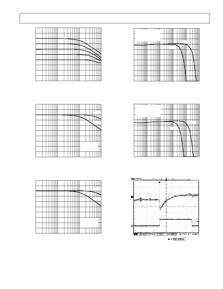
FREQUENCY ≠ Hz
I
DD
/I
SS
≠
A
500
10k
450
400
350
300
250
200
150
100
50
0
100k
1M
10M
CODE FF
H
I
SS
@ V
DD
/V
SS
= 2.5V
I
DD
@ V
DD
/V
SS
= 2.5V
I
DD
@ V
DD
/V
SS
= 5V/0V
I
DD
@ V
DD
/V
SS
= 3V/0V
TPC 13. AD5200 10 k
Supply Current vs. Clock Frequency
FREQUENCY ≠ Hz
I
DD
/I
SS
≠
A
500
10k
450
400
350
300
250
200
150
100
50
0
100k
1M
10M
CODE 55
H
I
SS
@ V
DD
/V
SS
= 2.5V
I
DD
@ V
DD
/V
SS
= 2.5V
I
DD
@ V
DD
/V
SS
= 5V/0V
I
DD
@ V
DD
/V
SS
= 3V/0V
TPC 14. AD5200 10 k
Supply Current vs. Clock Frequency
FREQUENCY ≠ Hz
PSRR
≠
dB
100
1k
10k
1M
+PSRR
@ V
DD
= 5V DC 10% p-p AC
100k
+PSRR
@ V
DD
= 3V DC 10% p-p AC
≠PSRR
@ V
DD
= 3V DC 10% p-p AC
CODE = 80
H
, V
A
= V
DD
, V
B
= 0V
80
60
40
20
0
TPC 15. Power Supply Rejection Ratio vs. Frequency
FREQUENCY ≠ Hz
6
≠54
GAIN
≠
dB
1k
10k
100k
1M
≠48
≠42
≠36
≠30
≠24
≠18
≠12
≠6
0
80
H
40
H
20
H
10
H
08
H
04
H
02
H
01
H
TPC 16. AD5200 10 k
Gain vs. Frequency vs. Code
FREQUENCY ≠ Hz
6
≠54
GAIN
≠
dB
1k
10k
100k
1M
≠48
≠42
≠36
≠30
≠24
≠18
≠12
≠6
0
80
H
40
H
20
H
10
H
08
H
04
H
02
H
01
H
TPC 17. AD5200 50 k
Gain vs. Frequency vs. Code
FREQUENCY ≠ Hz
6
≠54
GAIN
≠
dB
1k
10k
100k
1M
≠48
≠42
≠36
≠30
≠24
≠18
≠12
≠6
0
10
H
8
H
4
H
2
H
1
H
TPC 18. AD5201 10 k
Gain vs. Frequency vs. Code
REV. B
AD5200/AD5201
≠9≠
FREQUENCY ≠ Hz
6
≠54
GAIN
≠
dB
1k
10k
100k
1M
≠48
≠42
≠36
≠30
≠24
≠18
≠12
≠6
0
10
H
8
H
4
H
2
H
1
H
TPC 19. AD5201 50 k
Gain vs. Frequency vs. Code
FREQUENCY ≠ Hz
12
≠48
GAIN
≠
dB
1k
10k
100k
1M
≠42
≠36
≠30
≠24
≠18
≠12
≠6
0
6
10k
V
IN
= 100mV rms
V
DD
= 5V
R
L
= 1M
50k
TPC 20. AD5200 ≠3 dB Bandwidth
FREQUENCY ≠ Hz
12
≠48
GAIN
≠
dB
1k
10k
100k
1M
≠42
≠36
≠30
≠24
≠18
≠12
≠6
0
6
10k
V
IN
= 100mV rms
V
DD
= 5V
R
L
= 1M
50k
TPC 21. AD5201 ≠3 dB Bandwidth
FREQUENCY ≠ Hz
12
≠48
NORMALIZED GAIN FLATNESS
≠
0.1dB/DIV
10
10k
100k
1M
≠42
≠36
≠30
≠24
≠18
≠12
≠6
0
6
100
1k
50k
10k
SEE TEST CIRCUIT 10
CODE = 80
H
V
DD
= 5V
T
A
= 25 C
TPC 22. Normalized Gain Flatness vs. Frequency
FREQUENCY ≠ Hz
12
≠48
NORMALIZED GAIN FLATNESS
≠
0.1dB/DIV
10
10k
100k
1M
≠42
≠36
≠30
≠24
≠18
≠12
≠6
0
6
100
1k
50k
10k
SEE TEST CIRCUIT 10
CODE = 10
H
V
DD
= 5V
T
A
= 25 C
TPC 23. AD5201 Normalized Gain Flatness vs. Frequency
V
W
(20mV/DIV)
CS
(5V/DIV)
TPC 24. One Position Step Change at Half Scale
REV. B
AD5200/AD5201
≠10≠
OUTPUT
(2V/DIV)
INPUT
(5V/DIV)
TPC 25. Large Signal Settling Time
V
OUT
(20mV/DIV)
TPC 26. Digital Feedthrough vs. Time
CODE ≠ Decimal
4000
500
POTENTIOMETER MODE TEMPCO
≠
ppm/
C
0
3500
3000
2500
2000
1500
1000
500
0
32
64
96
128
160
192
224
256
TPC 27. AD5200
V
WB
/
T Potentiometer Mode
Temperature Coefficient
CODE ≠ Decimal
500
RHEOSTAT MODE TEMPCO
≠
ppm/
C
0
3500
3000
2500
2000
1500
1000
500
0
32
64
96
128
160
192
224
256
TPC 28. AD5200
R
WB
/
T Rheostat Mode Temperature
Coefficient
CODE ≠ Decimal
POTENTIOMETER MODE TEMPCO
≠
ppm/
C
3000
0
2500
2000
1500
1000
500
0
≠500
4
8
12
16
20
24
28
32
TPC 29. AD5201 Potentiometer Mode Temperature
Coefficient
CODE ≠ Decimal
POTENTIOMETER MODE TEMPCO
≠
ppm/
C
50
0
40
30
20
10
0
≠20
4
8
12
16
20
24
28
32
≠10
TPC 30. AD5201
V
WB
/
T Potentiometer Mode Tempco
REV. B
AD5200/AD5201
≠11≠
CODE ≠ Decimal
100.0
10.0
0.1
0
32
THEORETICAL I
MAX
≠
mA
1.0
64
96
128
160
192
224
256
R
AB
= 10k
R
AB
= 50k
TPC 31. AD5200 I
MAX
vs. Code
CODE ≠ Decimal
100.0
10.0
0.1
0
4
THEORETICAL I
MAX
≠
mA
1.0
8
12
16
20
24
28
32
R
AB
= 10k
R
AB
= 50k
TPC 32. AD5201 I
MAX
vs. Code
OPERATION
The AD5200/AD5201 provide 255 and 33 positions digitally-
controlled variable resistor (VR) devices. Changing the
programmed VR settings is accomplished by clocking in an 8-bit
serial data word for AD5200, and a 6-bit serial data word for
AD5201, into the SDI (Serial Data Input) pins. Table I provides
the serial register data word format. The AD5200/AD5201 are
preset to a midscale internally during power-on condition. In
addition, the AD5200/AD5201 contain power shutdown
SHDN pins that place the RDAC in a zero power consump-
tion state where the immediate switches next to Terminals A and
B are open-circuited. Meanwhile, the wiper W is connected to B
terminal, resulting in only leakage current consumption in the VR
structure. During shutdown, the VR latch contents are maintained
when the RDAC is inactive. When the part is returned from
shutdown, the stored VR setting will be applied to the RDAC.
Table I. AD5200 Serial-Data Word Format
7
B
6
B
5
B
4
B
3
B
2
B
1
B
0
B
7
D
6
D
5
D
4
D
3
D
2
D
1
D
0
D
B
S
M
B
S
L
2
7
2
0
Table II. AD5201 Serial-Data Word Format
5
B
*
4
B
3
B
2
B
1
B
0
B
5
D
*
4
D
3
D
2
D
1
D
0
D
B
S
M
B
S
L
2
5
2
0
*Six data bits are needed for 33 positions.
PROGRAMMING THE VARIABLE RESISTOR
Rheostat Operation
The nominal resistance of the RDAC between Terminals A and
B are available with values of 10 k
and 50 k. The final two
digits of the part number determine the nominal resistance
value, e.g., 10 k
= 10 and 50 k = 50. The nominal resistance
(R
AB
) of AD5200 has 256 contact points accessed by the wiper
terminal. The 8-bit data word in the RDAC latch of AD5200 is
decoded to select one of the 256 possible settings. In both parts,
the wiper's first connection starts at the B terminal for data 00
H
.
This B-terminal connection has a wiper contact resistance of
50
as long as valid V
DD
/V
SS
is applied, regardless of the nominal
resistance. For a 10 k
part, the second connection of AD5200 is
the first tap point with 89
[R
WB
= R
AB
/255 + R
W
= 39
+ 50 ]
for data 01
H
. The third connection is the next tap point representing
78 + 50 = 128
for data 02
H
. Due to its unique internal structure,
AD5201 has 5-bit + 1 resolution, but needs a 6-bit data word to
achieve the full 33 steps resolution. The 6-bit data word in the
RDAC latch is decoded to select one of the 33 possible settings.
Data 34 to 63 will automatically be equal to Position 33. The
wiper 00
H
connection of AD5201 gives 50
. Similarly, for a
10 k
part, the first tap point of AD5201 yields 363 for
data 01
H
, 675
for data 02
H
. For both AD5200 and AD5201,
each LSB data value increase moves the wiper up the resistor
ladder until the last tap point is reached. Figures 2a and 2b show
the simplified diagrams of the equivalent RDAC circuits.
REV. B
AD5200/AD5201
≠12≠
D7
D6
D5
D4
D3
D2
D1
D0
RDAC
LATCH &
DECODER
SHDN
SW
SHDN
SW
2
N
1
SW
2
N
2
SW
1
SW
0
A
R
R
R
B
W
DIGITAL CIRCUITRY
OMITTED FOR CLARITY
R
R
AB
2
N
≠1
Figure 2a. AD5200 Equivalent RDAC Circuit. 255 positions
can be achieved up to Switch SW
2
N
≠1
.
SW
2
N
1
D5
D4
D3
D2
D1
D0
RDAC
LATCH &
DECODER
SW
2
N
2
SW
1
SW
0
R
R
R
R
B
W
DIGITAL CIRCUITRY
OMITTED FOR CLARITY
SHDN
A
SW
SHDN
SW
2
N
R
R
AB
2
N
Figure 2b. AD5201 Equivalent RDAC Circuit. Unlike AD5200,
33 positions can be achieved all the way to Switch SW
2
N
.
The general equation determining the digitally programmed
output resistance between W and B is:
R
D
D
R
WB
AB
( )
=
+
255
50
for AD5200
(1)
R
D
D
R
WB
AB
( )
=
+
32
50
for AD5201
(2)
where:
D
is the decimal equivalent of the data contained in
RDAC latch.
R
AB
is the nominal end-to-end resistance.
R
W
is the wiper resistance contributed by the on-resistance
of the internal switch.
Note D in AD5200 is between 0 to 255 for 256 positions. On
the other hand, D in AD5201 is between 0 to 32 so that 33
positions can be achieved due to the slight internal structure
difference, Figure 2b.
Again if R
AB
= 10 k
and A terminal can be opened or tied to
W, the following output resistance between W to B will be set
for the following RDAC latch codes:
AD5200 Wiper-to-B Resistance
D
R
WB
(DEC)
( )
Output State
255
10050
Full-Scale (R
AB
+ R
W
)
128
5070
Midscale
1
89
1 LSB
0
50
Zero-Scale (Wiper Contact Resistance)
AD5201 Wiper-to-B Resistance
D
R
WB
(DEC)
( )
Output State
32
10050
Full-Scale (R
AB
+ R
W
)
16
5050
Midscale
1
363
1 LSB
0
50
Zero-Scale (Wiper Contact Resistance)
Note that in the zero-scale condition a finite wiper resistance of
50
is present. Care should be taken to limit the current flow
between W and B in this state to no more than
±20 mA to avoid
degradation or possible destruction of the internal switch contact.
Like the mechanical potentiometer the RDAC replaces, it is
totally symmetrical. The resistance between the wiper W and
Terminal A also produces a digitally controlled resistance R
WA
.
When these terminals are used, the B terminal should be tied to
the wiper. Setting the resistance value for R
WA
starts at a maxi-
mum value of resistance and decreases as the data loaded in
the latch is increased in value. The general equation for this
operation is:
R
D
D
R
WA
AB
( )
=
-
(
)
+
255
255
50
for AD5200
(3)
R
D
D
R
WA
AB
( )
=
-
(
)
+
32
32
50
for AD5201
(4)
Similarly, D in AD5200 is between 0 to 255, whereas D in
AD5201 is between 0 to 32.
For R
AB
= 10 k
and B terminal is opened or tied to the wiper
W, the following output resistance between W and A will be set
for the following RDAC latch codes:
REV. B
AD5200/AD5201
≠13≠
AD5200 Wiper-to-A Resistance
D
R
WA
(DEC)
( )
Output State
255
50
Full-Scale (R
W
)
128
5030
Midscale
1
10011
1 LSB
0
10050
Zero-Scale (R
AB
+ R
W
)
AD5201 Wiper-to-A Resistance
D
R
WA
(DEC)
( )
Output State
32
50
Full-Scale (R
W
)
16
5050
Midscale
1
9738
1 LSB
0
10050
Zero-Scale (R
AB
+ R
W
)
The tolerance of the nominal resistance can be
±30% due to
process lot dependance. If users apply the RDAC in rheostat
(variable resistance) mode, they should be aware of such specifi-
cation of tolerance. The change in R
AB
with temperature has a
500 ppm/
∞C temperature coefficient.
PROGRAMMING THE POTENTIOMETER DIVIDER
Voltage Output Operation
The digital potentiometer easily generates output voltages at
wiper-to-B and wiper-to-A to be proportional to the input volt-
age at A to B.
Unlike the polarity of V
DD
≠ V
SS
, which must be positive, volt-
age across A≠B, W≠A, and W≠B can be at either polarity.
If ignoring the effects of the wiper resistance for an approxima-
tion, connecting A terminal to 5 V and B terminal to ground
produces an output voltage at the wiper which can be any value
starting at almost zero to almost full scale with the minor devia-
tion contributed by the wiper resistance. Each LSB of voltage is
equal to the voltage applied across Terminal AB divided by the
2
N
-1
and 2
N
position resolution of the potentiometer divider for
AD5200 and AD5201 respectively. The general equation defin-
ing the output voltage with respect to ground for any valid input
voltage applied to Terminals A and B is:
V
D
D
V
V
W
AB
B
( )
=
+
255
for AD5200
(5)
V
D
D
V
V
W
AB
B
( )
=
+
32
for AD5201
(6)
where D in AD5200 is between 0 to 255 and D in AD5201 is
between 0 to 32.
For more accurate calculation, including the effects of wiper
resistance, V
W
can be found as:
V
D
R
D
R
V
R
D
R
V
W
WB
AB
A
WA
AB
B
( )
=
( )
+
( )
(7)
where R
WB
(D) and R
WA
(D) can be obtained from Equations
1 to 4.
Operation of the digital potentiometer in the divider mode results
in more accurate operation over temperature. Here the output
voltage is dependent on the ratio of the internal resistors and not
the absolute values; therefore, the drift reduces to 15 ppm/
∞C.
DIGITAL INTERFACING
The AD5200/AD5201 contain a standard three-wire serial input
control interface. The three inputs are clock (CLK),
CS, and
serial data input (SDI). The positive-edge-sensitive CLK input
requires clean transitions to avoid clocking incorrect data into
the serial input register. Standard logic families work well. If
mechanical switches are used for product evaluation, they
should be debounced by a flip-flop or other suitable means.
Figure 3 shows more detail of the internal digital circuitry. When
CS is low, the clock loads data into the serial register on each
positive clock edge (see Table III).
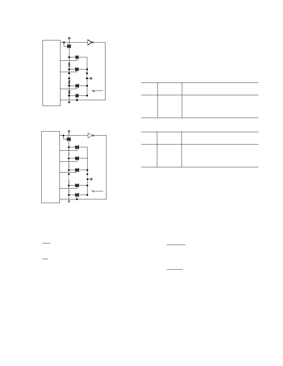
SER
REG
PWR-ON
PRESET
V
SS
A
W
B
SHDN
RDAC
REG
Dx
8/6
V
DD
CS
CLK
SDI
GND
AD5200/AD5201
Figure 3. Block Diagram
Table III. Input Logic Control Truth Table
CLK
CS
SHDN
Register Activity
L
L
H
No SR effect.
P
L
H
Shift one bit in from the SDI pin.
X
P
H
Load SR data into RDAC latch.
X
H
H
No operation.
X
H
L
Open circuit on A terminal and short
circuit between W to B terminals.
NOTE
P = positive edge, X = don't care, SR = shift register.
All digital inputs are protected with a series input resistor and
parallel Zener ESD structure shown in Figure 4. Applies to
digital input pins
CS, SDI, SHDN, CLK.
340
LOGIC
V
SS
Figure 4. ESD Protection of Digital Pins
A,B,W
V
SS
Figure 5. ESD Protection of Resistor Terminals
REV. B
AD5200/AD5201
≠14≠
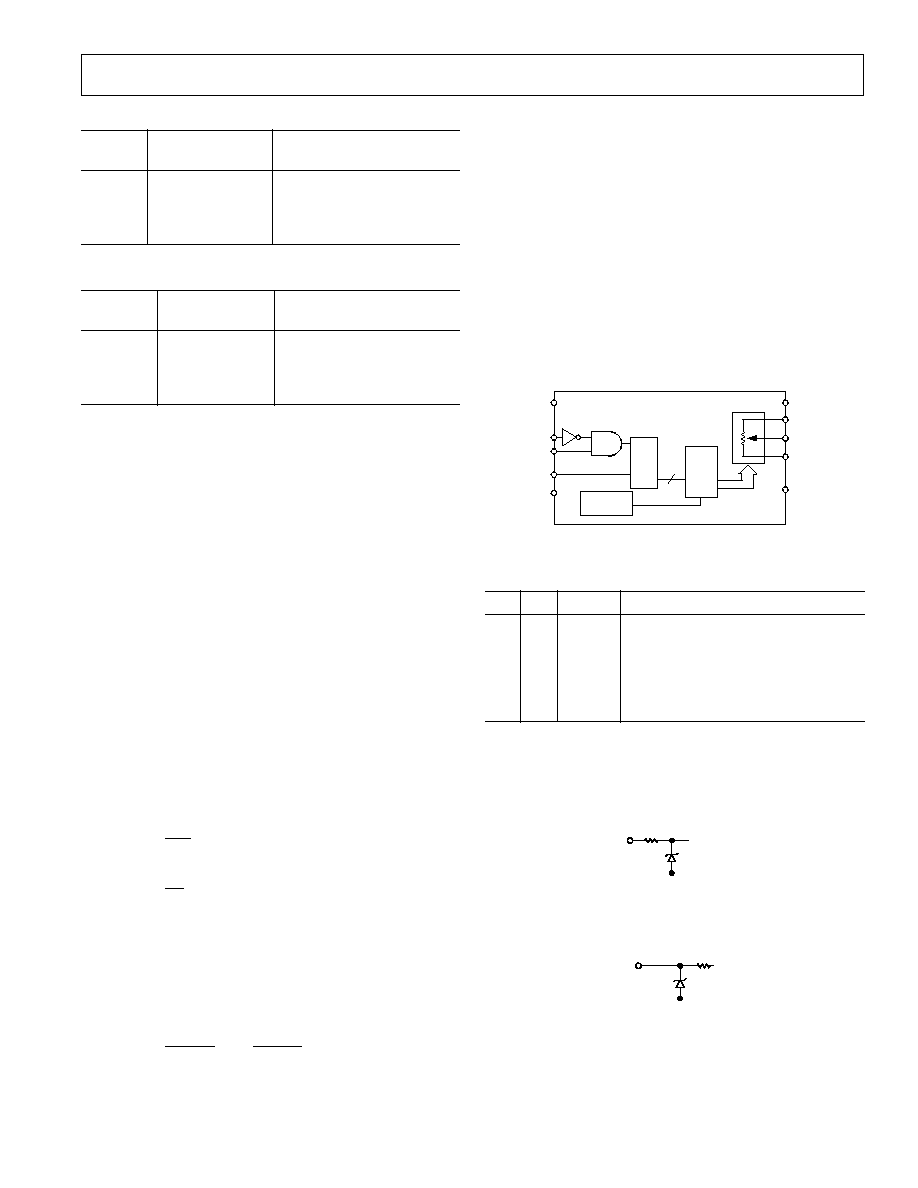
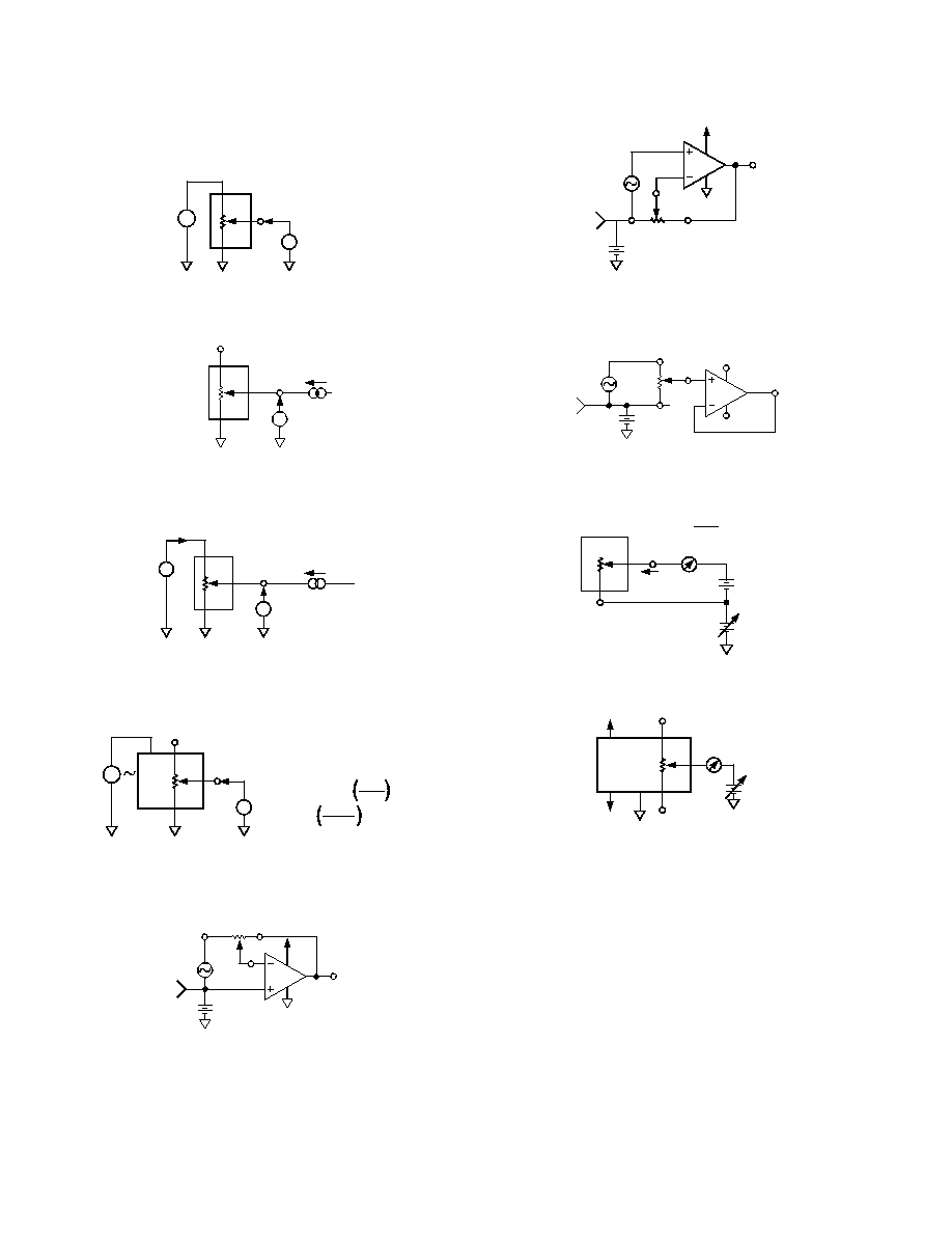
TEST CIRCUITS
Figures 6 to 14 define the test conditions used in the product
specification table.
V
MS
A
W
B
DUT
V+
V+
= V
DD
1 LSB = V+/2
N
Figure 6. Potentiometer Divider Nonlinearity Error Test
Circuit (INL, DNL)
V
MS
A
W
B
DUT
NO CONNECT
I
W
Figure 7. Resistor Position Nonlinearity Error
(Rheostat Operation; R-INL, R-DNL)
V
MS1
A
W
B
DUT
I
W
= V
DD
/R
NOMINAL
V
MS2
V
W
R
W
= [V
MS1
≠ V
MS2
]/I
W
Figure 8. Wiper Resistance Test Circuit
V
MS
%
V
DD
%
PSS (%/%) =
V+ = V
DD
10%
PSRR (dB) = 20 LOG
V
MS
V
DD
V
MS
A
W
B
V+
V
DD
V
A
Figure 9. Power Supply Sensitivity Test Circuit
(PSS, PSRR)
OP279
W
5V
B
V
OUT
OFFSET
GND
OFFSET BIAS
A
DUT
V
IN
Figure 10. Inverting Gain Test Circuit
OFFSET BIAS
B
OFFSET
GND
A
DUT
OP279
W
5V
V
OUT
V
IN
Figure 11. Noninverting Gain Test Circuit
OP42
V
OUT
V
IN
+15V
OFFSET
GND
≠15V
W
B
A
2.5V
Figure 12. Gain vs. Frequency Test Circuit
W
B
V
SS
TO V
DD
DUT
I
SW
CODE = OO
H
R
SW
=
0.1V
I
SW
0.1V
+
≠
Figure 13. Incremental ON Resistance Test Circuit
I
CM
A
W
B
NC
GND
NC
V
SS
V
DD
DUT
V
CM
NC = NO CONNECT
Figure 14. Common-Mode Leakage Current Test Circuit

REV. B
AD5200/AD5201
≠15≠
DIGITAL POTENTIOMETER SELECTION GUIDE
Number
Resolution
Power
of VRs
Terminal
Interface
Nominal
(Number
Supply
Part
per
Voltage
Data
Resistance
Of Wiper
Current
Number
Package
Range
Control
(k )
Positions)
(I
DD
)
Packages
Comments
AD5201
1
±3 V, +5.5 V
3-Wire
10, 50
33
60
µA
µSOIC-10
Full AC Specs, Dual Supply,
Pwr-On-Reset, Low Cost
AD5220
1
5.5 V
Up/Down
10, 50, 100
128
40
µA
PDIP, SO-8,
µSOIC-8 No Rollover, Pwr-On-Reset
AD7376
1
±15 V, +28 V
3-Wire
10, 50, 100, 1000
128
100
µA
PDIP-14, SOL-16,
Single 28 V or Dual
±15 V
TSSOP-14
Supply Operation
AD5200
1
±3 V, +5.5 V
3-Wire
10, 50
256
60
µA
µSOIC-10
Full AC Specs, Dual Supply,
Pwr-On-Reset
AD8400
1
5.5 V
3-Wire
1, 10, 50, 100
256
5
µA
SO-8
Full AC specs
AD5241
* 1
±3 V, +5.5 V
2-Wire
10, 100, 1000
256
5
µA
SO-14, TSSOP-14
I
2
C-Compatible, TC
< 50 ppm/
∞C
AD5231
* 1
±3 V, +5.5 V
3-Wire
10, 50, 100
1024
10
µA
TSSOP-16
Nonvolatile Memory, Direct
Program, I/D,
±6 dB Settability
AD5222
2
±3 V, +5.5 V
Up/Down
10, 50, 100, 1000
128
80
µA
SO-14, TSSOP-14
No Rollover, Stereo, Pwr-On-
Reset, TC < 50 ppm/
∞C
AD8402
2
5.5 V
3-Wire
1, 10, 50, 100
256
5
µA
PDIP, SO-14,
Full AC Specs, nA
TSSOP-14
Shutdown Current
AD5232
* 2
±3 V, +5.5 V
3-Wire
10, 50, 100
256
10
µA
TSSOP-16
Nonvolatile Memory, Direct
Program, I/D,
±6 dB Settability
AD5242
* 2
±3 V, +5.5 V
2-Wire
10, 100, 1000
256
5
µA
SO-16, TSSOP-16
I
2
C-Compatible, TC
< 50 ppm/
∞C
AD5262
* 2
±5 V, +12 V
3-Wire
10, 50, 100
256
60
µA
TSSOP-16
Medium Voltage Operation,
TC < 50 ppm/
∞C
AD5203
4
5.5 V
3-Wire
10, 100
64
5
µA
PDIP, SOL-24,
Full AC specs, nA
TSSOP-24
Shutdown Current
AD5233
* 4
±3 V, +5.5 V
3-Wire
10, 50, 100
64
10
µA
TSSOP-16
Nonvolatile Memory, Direct
Program, I/D,
±6 dB Settability
AD5204
4
±3 V, +5.5 V
3-Wire
10, 50, 100
256
5
µA
PDIP, SOL-24,
Full AC Specs, Dual Supply,
TSSOP-24
Pwr-On-Reset
AD8403
4
5.5 V
3-Wire
1, 10, 50, 100
256
5
µA
PDIP, SOL-24,
Full AC Specs, nA
TSSOP-24
Shutdown Current
AD5206
6
±3 V, +5.5 V
3-Wire
10, 50, 100
256
5
µA
PDIP, SOL-24,
Full AC Specs, Dual Supply,
TSSOP-24
Pwr-On-Reset
*Future product, consult factory for latest status.
≠16≠
C02188≠0≠8/01(B)
PRINTED IN U.S.A.
REV. B
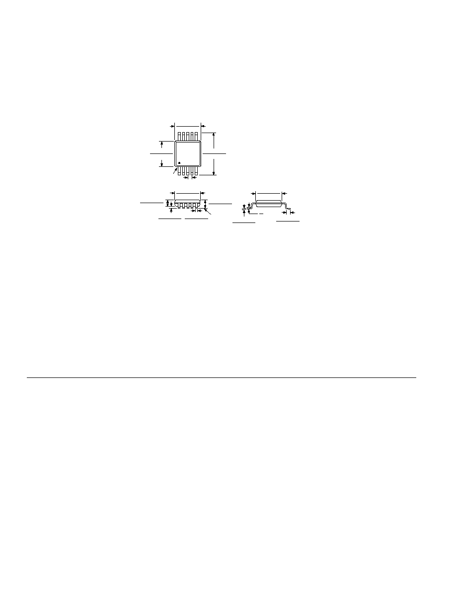
10-Lead SOIC
(RM-10)
0.011 (0.28)
0.003 (0.08)
0.120 (3.05)
0.112 (2.84)
0.022 (0.56)
0.021 (0.53)
6
0
10
6
5
1
0.0197 (0.50) BSC
0.124 (3.15)
0.112 (2.84)
0.124 (3.15)
0.112 (2.84)
0.199 (5.05)
0.187 (4.75)
PIN 1
0.122 (3.10)
0.110 (2.79)
0.006 (0.15)
0.002 (0.05)
0.016 (0.41)
0.006 (0.15)
0.038 (0.97)
0.030 (0.76)
SEATING
PLANE
0.043 (1.09)
0.037 (0.94)
OUTLINE DIMENSIONS
Dimensions shown in inches and (mm).
AD5200/AD5201
Revision History
Location
Page
Data Sheet changed from REV. A to REV. B.
Edits to ORDERING GUIDE . . . . . . . . . . . . . . . . . . . . . . . . . . . . . . . . . . . . . . . . . . . . . . . . . . . . . . . . . . . . . . . . . . . . . . . . . . . . . . 5
02/01--Data Sheet changed from REV. O to REV. A.
Edits to ORDERING GUIDE . . . . . . . . . . . . . . . . . . . . . . . . . . . . . . . . . . . . . . . . . . . . . . . . . . . . . . . . . . . . . . . . . . . . . . . . . . . . . 5
Edits to ABSOLUTE MAXIMUM RATINGS . . . . . . . . . . . . . . . . . . . . . . . . . . . . . . . . . . . . . . . . . . . . . . . . . . . . . . . . . . . . . . . . 5
TPCs 31 and 32 added . . . . . . . . . . . . . . . . . . . . . . . . . . . . . . . . . . . . . . . . . . . . . . . . . . . . . . . . . . . . . . . . . . . . . . . . . . . . . . . . . 11