Information furnished by Analog Devices is believed to be accurate and
reliable. However, no responsibility is assumed by Analog Devices for its
use, nor for any infringements of patents or other rights of third parties
which may result from its use. No license is granted by implication or
otherwise under any patent or patent rights of Analog Devices.
a
AD5204/AD5206
One Technology Way, P.O. Box 9106, Norwood, MA 02062-9106, U.S.A.
Tel: 781/329-4700
World Wide Web Site: http://www.analog.com
Fax: 781/326-8703
© Analog Devices, Inc., 1999
REV. 0
4-/6-Channel
Digital Potentiometers
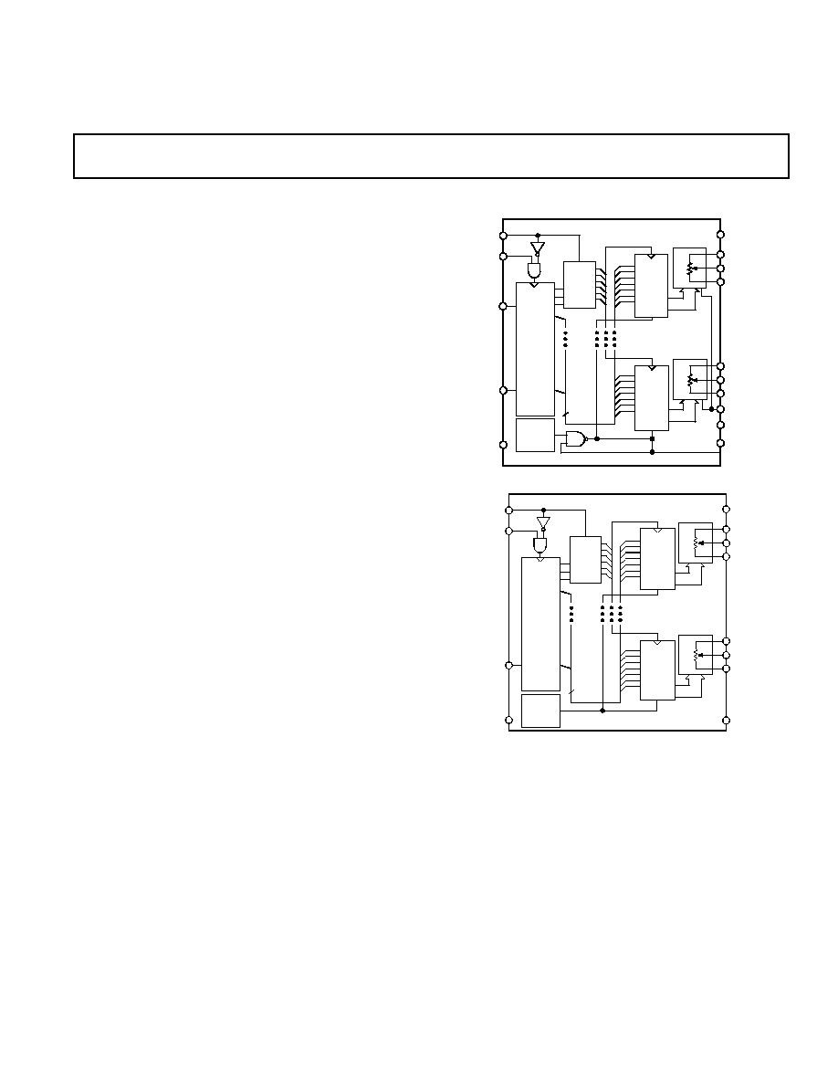
FUNCTIONAL BLOCK DIAGRAMS
D7
D0
A1
W1
B1
V
DD
AD5204
CS
CLK
8
EN
ADDR
DEC
A2
A1
A0
SDI
DI
SER
REG
D0
D7
A4
W4
B4
GND
RDAC
LATCH
#1
R
D7
D0
RDAC
LATCH
#4
R
POWER-
ON
PRESET
V
SS
SDO
DO
PR
SHDN
D7
D0
A1
W1
B1
V
DD
AD5206
CS
CLK
8
EN
ADDR
DEC
A2
A1
A0
SDI
DI
SER
REG
D0
D7
A6
W6
B6
GND
RDAC
LATCH
#1
R
D7
D0
RDAC
LATCH
#6
R
POWER-
ON
PRESET
V
SS
FEATURES
256 Position
Multiple Independently Programmable Channels
AD5204--4-Channel
AD5206--6-Channel
Potentiometer Replacement
10 k , 50 k , 100 k
3-Wire SPI-Compatible Serial Data Input
+2.7 V to +5.5 V Single Supply; 2.7 V Dual Supply
Operation
Power ON Midscale Preset
APPLICATIONS
Mechanical Potentiometer Replacement
Instrumentation: Gain, Offset Adjustment
Programmable Voltage-to-Current Conversion
Programmable Filters, Delays, Time Constants
Line Impedance Matching
GENERAL DESCRIPTION
The AD5204/AD5206 provides four-/six-channel, 256 position
digitally-controlled Variable Resistor (VR) devices. These de-
vices perform the same electronic adjustment function as a
potentiometer or variable resistor. Each channel of the AD5204/
AD5206 contains a fixed resistor with a wiper contact that taps
the fixed resistor value at a point determined by a digital code
loaded into the SPI-compatible serial-input register. The resis-
tance between the wiper and either endpoint of the fixed resistor
varies linearly with respect to the digital code transferred into
the VR latch. The variable resistor offers a completely program-
mable value of resistance between the A terminal and the wiper
or the B Terminal and the wiper. The fixed A-to-B terminal
resistance of 10 k
, 50 k
, or 100 k
has a nominal tempera-
ture coefficient of 700 ppm/
∞
C.
Each VR has its own VR latch which holds its programmed
resistance value. These VR latches are updated from an internal
serial-to-parallel shift register that is loaded from a standard
3-wire serial-input digital interface. Eleven data bits make up
the data word clocked into the serial input register. The first
three bits are decoded to determine which VR latch will be
loaded with the last eight bits of the data word when the
CS
strobe is returned to logic high. A serial data output pin at
the opposite end of the serial register (AD5204 only) allows
simple daisy-chaining in multiple VR applications without
additional external decoding logic.
An optional reset (
PR) pin forces all the AD5204 wipers to the
midscale position by loading 80
H
into the VR latch.
The AD5204/AD5206 is available in both surface mount
(SOL-24), TSSOP-24 and the 24-lead plastic DIP package. All
parts are guaranteed to operate over the extended industrial
temperature range of ≠40
∞
C to +85
∞
C. For additional single,
dual, and quad channel devices, see the AD8400/AD8402/
AD8403 products.

REV. 0
AD5204/AD5206≠SPECIFICATIONS
≠2≠
ELECTRICAL CHARACTERISTICS
Parameter
Symbol
Conditions
Min
Typ
1
Max
Units
DC CHARACTERISTICS RHEOSTAT MODE Specifications Apply to All VRs
Resistor Differential NL
2
R-DNL
R
WB
, V
A
= No Connect
≠1
±
1/4
+1
LSB
Resistor Nonlinearity Error
2
R-INL
R
WB
, V
A
= No Connect
≠2
±
1/2
+2
LSB
Nominal Resistor Tolerance
3
R
AB
T
A
= +25
∞
C
≠30
+30
%
Resistance Temperature Coefficient
R
AB
/
T
V
AB
= V
DD
, Wiper = No Connect
700
ppm/
∞
C
Nominal Resistance Match
R/R
AB
CH1 to 2, 3, 4, or 5, 6; V
AB
= V
DD
0.25
1.5
%
Wiper Resistance
R
W
I
W
= 1 V/R, V
DD
= +5 V
50
100
DC CHARACTERISTICS POTENTIOMETER DIVIDER MODE Specifications Apply to All VRs
Resolution
N
8
Bits
Differential Nonlinearity
4
DNL
≠1
±
1/4
+1
LSB
Integral Nonlinearity
4
INL
≠2
±
1/2
+2
LSB
Voltage Divider Temperature Coefficient
V
W
/
T
Code = 40
H
15
ppm/
∞
C
Full-Scale Error
V
WFSE
Code = 7F
H
≠2
≠1
0
LSB
Zero-Scale Error
V
WZSE
Code = 00
H
0
+1
+2
LSB
RESISTOR TERMINALS
Voltage Range
5
V
A,
V
B,
V
W
V
SS
V
DD
V
Capacitance
6
Ax, Bx
C
A,
C
B
f = 1 MHz, Measured to GND, Code = 40
H
45
pF
Capacitance
6
Wx
C
W
f = 1 MHz, Measured to GND, Code = 40
H
60
pF
Shutdown Current
7
I
A_SD
0.01
5
µ
A
Common-Mode Leakage
I
CM
V
A
= V
B
= V
W
= 0, V
DD
= +2.7 V, V
SS
= ≠2.5 V
1
nA
DIGITAL INPUTS AND OUTPUTS
Input Logic High
V
IH
V
DD
= +5 V/+3 V
2.4/2.1
V
Input Logic Low
V
IL
V
DD
= +5 V/+3 V
0.8/0.6
V
Output Logic High
V
OH
R
PULL≠UP
= 1 k
to +5 V
4.9
V
Output Logic Low
V
OL
I
OL
= 1.6 mA, V
LOGIC
= +5 V
0.4
V
Input Current
I
IL
V
IN
= 0 V or +5 V
±
1
µ
A
Input Capacitance
6
C
IL
5
pF
POWER SUPPLIES
Power Single Supply Range
V
DD
Range
V
SS
= 0 V
2.7
5.5
V
Power Dual Supply Range
V
DD/SS
Range
±
2.3
±
2.7
V
Positive Supply Current
I
DD
V
IH
= +5 V or V
IL
= 0 V
12
60
µ
A
Negative Supply Current
I
SS
V
SS
= ≠2.5 V, V
DD
= +2.7 V
12
60
µ
A
Power Dissipation
8
P
DISS
V
IH
= +5 V or V
IL
= 0 V
0.3
mW
Power Supply Sensitivity
PSS
V
DD
= +5 V
±
10%
0.0002
0.005
%/%
DYNAMIC CHARACTERISTICS
6, 9
Bandwidth ≠3 dB
BW_10K
R
AB
= 10 k
721
kHz
BW_50K
R
AB
= 50 k
137
kHz
BW_100K
R
AB
= 100 k
69
kHz
Total Harmonic Distortion
THD
W
V
A
= 1.414 V rms, V
B
= 0 V dc, f = 1 kHz
0.004
%
V
W
Settling Time (10K/50K/100K)
t
S
V
A
= 5 V, V
B
= 0 V,
±
1 LSB Error Band
2/9/18
µ
s
Resistor Noise Voltage
e
N_WB
R
WB
= 5 k
, f = 1 kHz,
PR = 0
9
nV/
Hz
INTERFACE TIMING CHARACTERISTICS Applies to All Parts
6, 10
Input Clock Pulsewidth
t
CH
, t
CL
Clock Level High or Low
20
ns
Data Setup Time
t
DS
5
ns
Data Hold Time
t
DH
5
ns
CLK to SDO Propagation Delay
11
t
PD
R
L
= 2 k
, C
L
< 20 pF
1
150
ns
CS Setup Time
t
CSS
15
ns
CS High Pulsewidth
t
CSW
40
ns
Reset Pulsewidth
t
RS
90
ns
CLK Fall to
CS Fall Setup
t
CSH0
0
ns
CLK Fall to
CS Rise Hold Time
t
CSH1
0
ns
CS Rise to Clock Rise Setup
t
CS1
10
ns
NOTES
1
Typicals represent average readings at +25
∞
C and V
DD
= +5 V.
2
Resistor position nonlinearity error R-INL is the deviation from an ideal value measured between the maximum resistance and the minimum resistance wiper posi-
tions. R-DNL measures the relative step change from ideal between successive tap positions. Parts are guaranteed monotonic. See Figure 23 test circuit. I
W
= V
DD
/R
for both V
DD
= +3 V or V
DD
= +5 V.
3
V
AB
= V
DD
, Wiper (V
W
) = No connect.
4
INL and DNL are measured at V
W
with the RDAC configured as a potentiometer divider similar to a voltage output D/A converter. V
A
= V
DD
and V
B
= 0 V.
DNL specification limits of
±
1 LSB maximum are guaranteed monotonic operating conditions. See Figure 22 test circuit.
(V
DD
= +5 V 10% or +3 V 10%, V
SS
= 0 V, V
A
= +V
DD
, V
B
= 0 V, ≠40 C < T
A
< +85 C
unless otherwise noted.)

≠3≠
AD5204/AD5206
REV. 0
5
Resistor Terminals A, B, W, have no limitations on polarity with respect to each other.
6
Guaranteed by design and not subject to production test.
7
Measured at the Ax terminals. All Ax terminals are open-circuited in shutdown mode.
8
P
DISS
is calculated from (I
DD
◊
V
DD
). CMOS logic level inputs result in minimum power dissipation.
9
All dynamic characteristics use V
DD
= +5 V.
10
See timing diagrams for location of measured values. All input control voltages are specified with t
R
= t
F
= 2.5 ns (10% to 90% of 3 V) and timed from a voltage
level of 1.5 V. Switching characteristics are measured using both V
DD
= +3 V or +5 V.
11
Propagation delay depends on value of V
DD
, R
L
and C
L
. See Operation section.
Specifications subject to change without notice.
ABSOLUTE MAXIMUM RATINGS*
(T
A
= +25
∞
C, unless otherwise noted)
V
DD
to GND . . . . . . . . . . . . . . . . . . . . . . . . . . . . ≠0.3 V, +7 V
V
SS
to GND . . . . . . . . . . . . . . . . . . . . . . . . . . . . . . . 0 V, ≠7 V
V
DD
to V
SS
. . . . . . . . . . . . . . . . . . . . . . . . . . . . . . . . . . . +7 V
V
A
, V
B
, V
W
to GND . . . . . . . . . . . . . . . . . . . . . . . . . . V
SS
, V
DD
Ax≠Bx, Ax≠Wx, Bx≠Wx . . . . . . . . . . . . . . . . . . . . . .
±
20 mA
Digital Input and Output Voltage to GND . . . . . . . 0 V, +7 V
Operating Temperature Range . . . . . . . . . . . ≠40
∞
C to +85
∞
C
Maximum Junction Temperature (T
J
MAX) . . . . . . . . +150
∞
C
Storage Temperature . . . . . . . . . . . . . . . . . . ≠65
∞
C to +150
∞
C
Lead Temperature (Soldering, 10 sec) . . . . . . . . . . . . +300
∞
C
CAUTION
ESD (electrostatic discharge) sensitive device. Electrostatic charges as high as 4000 V readily
accumulate on the human body and test equipment and can discharge without detection.
Although the AD5204/AD5206 features proprietary ESD protection circuitry, permanent dam-
age may occur on devices subjected to high energy electrostatic discharges. Therefore, proper
ESD precautions are recommended to avoid performance degradation or loss of functionality.
Package Power Dissipation . . . . . . . . . . . . . . (T
J
max≠T
A
)/
JA
Thermal Resistance
JA
P-DIP (N-24) . . . . . . . . . . . . . . . . . . . . . . . . . . . . 63
∞
C/W
SOIC (SOL-24) . . . . . . . . . . . . . . . . . . . . . . . . . . . 70
∞
C/W
TSSOP-24 . . . . . . . . . . . . . . . . . . . . . . . . . . . . . . 143
∞
C/W
*Stresses above those listed under Absolute Maximum Ratings may cause perma-
nent damage to the device. This is a stress rating only; functional operation of the
device at these or any other conditions above those indicated in the operational
sections of this specification is not implied. Exposure to absolute maximum rating
conditions for extended periods may affect device reliability.
WARNING!
ESD SENSITIVE DEVICE

AD5204/AD5206
≠4≠
REV. 0
ORDERING GUIDE
Model
k
Temperature Range
Package Descriptions
Package Options
AD5204BN10
10
≠40
∞
C to +85
∞
C
24-Lead Narrow Body (PDIP)
N-24
AD5204BR10
10
≠40
∞
C to +85
∞
C
24-Lead Wide Body (SOIC)
R-24/SOL-24
AD5204BRU10
10
≠40
∞
C to +85
∞
C
24-Lead Thin Shrink SO Package (TSSOP)
RU-24
AD5204BN50
50
≠40
∞
C to +85
∞
C
24-Lead Narrow Body (PDIP)
N-24
AD5204BR50
50
≠40
∞
C to +85
∞
C
24-Lead Wide Body (SOIC)
R-24/SOL-24
AD5204BRU50
50
≠40
∞
C to +85
∞
C
24-Lead Thin Shrink SO Package (TSSOP)
RU-24
AD5204BN100
100
≠40
∞
C to +85
∞
C
24-Lead Narrow Body (PDIP)
N-24
AD5204BR100
100
≠40
∞
C to +85
∞
C
24-Lead Wide Body (SOIC)
R-24/SOL-24
AD5204BRU100
100
≠40
∞
C to +85
∞
C
24-Lead Thin Shrink SO Package (TSSOP)
RU-24
AD5206BN10
10
≠40
∞
C to +85
∞
C
24-Lead Narrow Body (PDIP)
N-24
AD5206BR10
10
≠40
∞
C to +85
∞
C
24-Lead Wide Body (SOIC)
R-24/SOL-24
AD5206BRU10
10
≠40
∞
C to +85
∞
C
24-Lead Thin Shrink SO Package (TSSOP)
RU-24
AD5206BN50
50
≠40
∞
C to +85
∞
C
24-Lead Narrow Body (PDIP)
N-24
AD5206BR50
50
≠40
∞
C to +85
∞
C
24-Lead Wide Body (SOIC)
R-24/SOL-24
AD5206BRU50
50
≠40
∞
C to +85
∞
C
24-Lead Thin Shrink SO Package (TSSOP)
RU-24
AD5206BN100
100
≠40
∞
C to +85
∞
C
24-Lead Narrow Body (PDIP)
N-24
AD5206BR100
100
≠40
∞
C to +85
∞
C
24-Lead Wide Body (SOIC)
R-24/SOL-24
AD5206BRU100
100
≠40
∞
C to +85
∞
C
24-Lead Thin Shrink SO Package (TSSOP)
RU
-24
The AD5204/AD5206 contains 5,925 transistors. Die size; 92 mil
◊
114 mil, 10,488 sq. mil.
SDI
CLK
CS
V
OUT
1
0
1
0
1
0
V
DD
0V
A2 A1 A0 D7 D6 D5 D4 D3 D2 D1 D0
RDAC LATCH LOAD
Figure 1. Timing Diagram
SDI
(DATA IN)
SDO
(DATA OUT)
1
0
1
0
1
0
1
0
V
DD
0V
CLK
CS
V
OUT
Ax OR Dx
Ax OR Dx
Ax OR Dx
Ax OR Dx
t
CSS
t
DH
t
PD_MAX
t
CSH0
1 LSB ERROR BAND
1 LSB
t
CSH1
t
CH
t
CSW
t
S
t
CL
t
DS
t
CS1
Figure 2. Detail Timing Diagram
PR
V
OUT
V
DD
1
0
0V
1 LSB
t
S
1 LSB ERROR BAND
t
RS
Figure 3. AD5204 Preset Timing Diagram
AD5204/AD5206
≠5≠
REV. 0
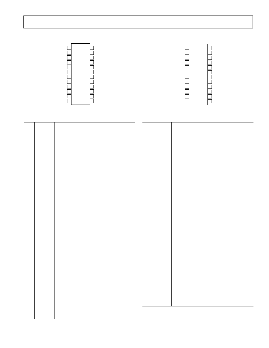
AD5204 PIN FUNCTION DESCRIPTIONS
Pin
No.
Name
Description
1, 2,
12
NC
Not Connected.
3
GND
Ground.
4
CS
Chip Select Input, Active Low. When
CS
returns high, data in the serial input register
is decoded based on the address bits and
loaded into the target RDAC latch.
5
PR
Active low preset to midscale; sets RDAC
registers to 80H.
6
V
DD
Positive power supply, specified for
operation at both +3 V or +5 V. (Sum of
|V
DD
| + |V
SS
| <5.5 V.)
7
SHDN
Active low input. Terminal A open-circuit.
Shutdown controls Variable Resistors #1
through #4.
8
SDI
Serial Data Input. MSB First.
9
CLK
Serial Clock Input, positive edge triggered.
10
SDO
Serial Data Output, Open Drain transistor
requires pull-up resistor.
11
V
SS
Negative Power Supply, specified for
operation at both 0 V or ≠2.7 V. (Sum of
|V
DD
| + |V
SS
| <5.5 V.)
13
B3
B Terminal RDAC #3.
14
W3
Wiper RDAC #3, addr = 010
2
.
15
A3
A Terminal RDAC #3.
16
B1
B Terminal RDAC #1.
17
W1
Wiper RDAC #1, addr = 000
2
.
18
A1
A Terminal RDAC #1.
19
A2
A Terminal RDAC #2.
20
W2
Wiper RDAC #2, addr = 001
2
.
21
B2
B Terminal RDAC #2.
22
A4
A Terminal RDAC #4.
23
W4
Wiper RDAC #4, addr = 011
2
.
24
B4
B Terminal RDAC #4.
AD5206 PIN FUNCTION DESCRIPTIONS
Pin
No.
Name
Description
1
A6
A Terminal RDAC #6.
2
W6
Wiper RDAC #6, addr = 101
2
.
3
B6
B Terminal RDAC #6.
4
GND
Ground.
5
CS
Chip Select Input, Active Low. When
CS
returns high, data in the serial input register
is decoded based on the address bits and
loaded into the target RDAC latch.
6
V
DD
Positive power supply, specified for
operation at both +3 V or +5 V. (Sum of
|V
DD
| + |V
SS
| <5.5 V.)
7
SDI
Serial Data Input. MSB First.
8
CLK
Serial Clock Input, positive edge triggered.
9
V
SS
Negative Power Supply, specified for
operation at both 0 V or ≠2.7 V. (Sum of
|V
DD
| + |V
SS
| <5.5 V.)
10
B5
B Terminal RDAC #5.
11
W5
Wiper RDAC #5, addr = 100
2
.
12
A5
A Terminal RDAC #5.
13
B3
B Terminal RDAC #3.
14
W3
Wiper RDAC #3, addr = 010
2
.
15
A3
A Terminal RDAC #3.
16
B1
B Terminal RDAC #1.
17
W1
Wiper RDAC #1, addr = 000
2
.
18
A1
A Terminal RDAC #1.
19
A2
A Terminal RDAC #2.
20
W2
Wiper RDAC #2, addr = 001
2
.
21
B2
B Terminal RDAC #2.
22
A4
A Terminal RDAC #4.
23
W4
Wiper RDAC #4, addr = 011
2
.
24
B4
B Terminal RDAC #4.
AD5206 PIN CONFIGURATION
24
23
22
21
20
19
18
17
16
15
14
13
1
2
3
4
5
6
7
8
9
10
11
12
A5
W5
B5
V
SS
CLK
A6
W6
B6
GND
SDI
V
DD
CS
B3
W3
A3
B1
W1
B4
W4
A4
B2
A1
A2
W2
AD5206
(NOT TO
SCALE)
AD5204 PIN CONFIGURATION
24
23
22
21
20
19
18
17
16
15
14
13
1
2
3
4
5
6
7
8
9
10
11
12
NC
V
SS
SDO
CLK
SDI
NC
NC
GND
CS
SHDN
V
DD
PR
B3
W3
A3
B1
W1
B4
W4
A4
B2
A1
A2
W2
AD5204
(NOT TO
SCALE)
NC = NO CONNECT