 | –≠–ª–µ–∫—Ç—Ä–æ–Ω–Ω—ã–π –∫–æ–º–ø–æ–Ω–µ–Ω—Ç: AD5204T | –°–∫–∞—á–∞—Ç—å:  PDF PDF  ZIP ZIP |
Information furnished by Analog Devices is believed to be accurate and
reliable. However, no responsibility is assumed by Analog Devices for its
use, nor for any infringements of patents or other rights of third parties
which may result from its use. No license is granted by implication or
otherwise under any patent or patent rights of Analog Devices.
a
AD5204/AD5206
One Technology Way, P.O. Box 9106, Norwood, MA 02062-9106, U.S.A.
Tel: 781/329-4700
World Wide Web Site: http://www.analog.com
Fax: 781/326-8703
© Analog Devices, Inc., 1999
REV. 0
4-/6-Channel
Digital Potentiometers
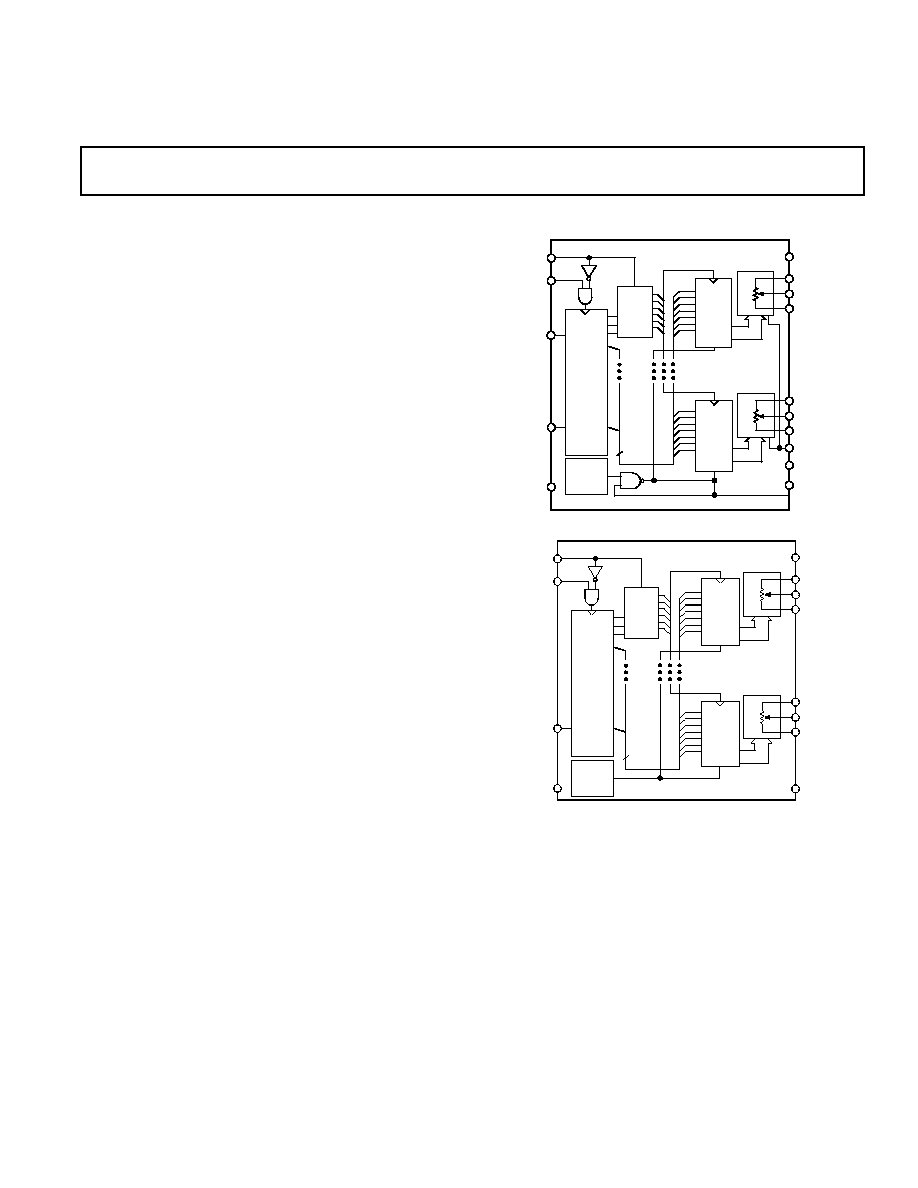
FUNCTIONAL BLOCK DIAGRAMS
D7
D0
A1
W1
B1
V
DD
AD5204
CS
CLK
8
EN
ADDR
DEC
A2
A1
A0
SDI
DI
SER
REG
D0
D7
A4
W4
B4
GND
RDAC
LATCH
#1
R
D7
D0
RDAC
LATCH
#4
R
POWER-
ON
PRESET
V
SS
SDO
DO
PR
SHDN
D7
D0
A1
W1
B1
V
DD
AD5206
CS
CLK
8
EN
ADDR
DEC
A2
A1
A0
SDI
DI
SER
REG
D0
D7
A6
W6
B6
GND
RDAC
LATCH
#1
R
D7
D0
RDAC
LATCH
#6
R
POWER-
ON
PRESET
V
SS
FEATURES
256 Position
Multiple Independently Programmable Channels
AD5204--4-Channel
AD5206--6-Channel
Potentiometer Replacement
10 k , 50 k , 100 k
3-Wire SPI-Compatible Serial Data Input
+2.7 V to +5.5 V Single Supply; 2.7 V Dual Supply
Operation
Power ON Midscale Preset
APPLICATIONS
Mechanical Potentiometer Replacement
Instrumentation: Gain, Offset Adjustment
Programmable Voltage-to-Current Conversion
Programmable Filters, Delays, Time Constants
Line Impedance Matching
GENERAL DESCRIPTION
The AD5204/AD5206 provides four-/six-channel, 256 position
digitally-controlled Variable Resistor (VR) devices. These de-
vices perform the same electronic adjustment function as a
potentiometer or variable resistor. Each channel of the AD5204/
AD5206 contains a fixed resistor with a wiper contact that taps
the fixed resistor value at a point determined by a digital code
loaded into the SPI-compatible serial-input register. The resis-
tance between the wiper and either endpoint of the fixed resistor
varies linearly with respect to the digital code transferred into
the VR latch. The variable resistor offers a completely program-
mable value of resistance between the A terminal and the wiper
or the B Terminal and the wiper. The fixed A-to-B terminal
resistance of 10 k
, 50 k
, or 100 k
has a nominal tempera-
ture coefficient of 700 ppm/
∞
C.
Each VR has its own VR latch which holds its programmed
resistance value. These VR latches are updated from an internal
serial-to-parallel shift register that is loaded from a standard
3-wire serial-input digital interface. Eleven data bits make up
the data word clocked into the serial input register. The first
three bits are decoded to determine which VR latch will be
loaded with the last eight bits of the data word when the
CS
strobe is returned to logic high. A serial data output pin at
the opposite end of the serial register (AD5204 only) allows
simple daisy-chaining in multiple VR applications without
additional external decoding logic.
An optional reset (
PR) pin forces all the AD5204 wipers to the
midscale position by loading 80
H
into the VR latch.
The AD5204/AD5206 is available in both surface mount
(SOL-24), TSSOP-24 and the 24-lead plastic DIP package. All
parts are guaranteed to operate over the extended industrial
temperature range of ≠40
∞
C to +85
∞
C. For additional single,
dual, and quad channel devices, see the AD8400/AD8402/
AD8403 products.

REV. 0
AD5204/AD5206≠SPECIFICATIONS
≠2≠
ELECTRICAL CHARACTERISTICS
Parameter
Symbol
Conditions
Min
Typ
1
Max
Units
DC CHARACTERISTICS RHEOSTAT MODE Specifications Apply to All VRs
Resistor Differential NL
2
R-DNL
R
WB
, V
A
= No Connect
≠1
±
1/4
+1
LSB
Resistor Nonlinearity Error
2
R-INL
R
WB
, V
A
= No Connect
≠2
±
1/2
+2
LSB
Nominal Resistor Tolerance
3
R
AB
T
A
= +25
∞
C
≠30
+30
%
Resistance Temperature Coefficient
R
AB
/
T
V
AB
= V
DD
, Wiper = No Connect
700
ppm/
∞
C
Nominal Resistance Match
R/R
AB
CH1 to 2, 3, 4, or 5, 6; V
AB
= V
DD
0.25
1.5
%
Wiper Resistance
R
W
I
W
= 1 V/R, V
DD
= +5 V
50
100
DC CHARACTERISTICS POTENTIOMETER DIVIDER MODE Specifications Apply to All VRs
Resolution
N
8
Bits
Differential Nonlinearity
4
DNL
≠1
±
1/4
+1
LSB
Integral Nonlinearity
4
INL
≠2
±
1/2
+2
LSB
Voltage Divider Temperature Coefficient
V
W
/
T
Code = 40
H
15
ppm/
∞
C
Full-Scale Error
V
WFSE
Code = 7F
H
≠2
≠1
0
LSB
Zero-Scale Error
V
WZSE
Code = 00
H
0
+1
+2
LSB
RESISTOR TERMINALS
Voltage Range
5
V
A,
V
B,
V
W
V
SS
V
DD
V
Capacitance
6
Ax, Bx
C
A,
C
B
f = 1 MHz, Measured to GND, Code = 40
H
45
pF
Capacitance
6
Wx
C
W
f = 1 MHz, Measured to GND, Code = 40
H
60
pF
Shutdown Current
7
I
A_SD
0.01
5
µ
A
Common-Mode Leakage
I
CM
V
A
= V
B
= V
W
= 0, V
DD
= +2.7 V, V
SS
= ≠2.5 V
1
nA
DIGITAL INPUTS AND OUTPUTS
Input Logic High
V
IH
V
DD
= +5 V/+3 V
2.4/2.1
V
Input Logic Low
V
IL
V
DD
= +5 V/+3 V
0.8/0.6
V
Output Logic High
V
OH
R
PULL≠UP
= 1 k
to +5 V
4.9
V
Output Logic Low
V
OL
I
OL
= 1.6 mA, V
LOGIC
= +5 V
0.4
V
Input Current
I
IL
V
IN
= 0 V or +5 V
±
1
µ
A
Input Capacitance
6
C
IL
5
pF
POWER SUPPLIES
Power Single Supply Range
V
DD
Range
V
SS
= 0 V
2.7
5.5
V
Power Dual Supply Range
V
DD/SS
Range
±
2.3
±
2.7
V
Positive Supply Current
I
DD
V
IH
= +5 V or V
IL
= 0 V
12
60
µ
A
Negative Supply Current
I
SS
V
SS
= ≠2.5 V, V
DD
= +2.7 V
12
60
µ
A
Power Dissipation
8
P
DISS
V
IH
= +5 V or V
IL
= 0 V
0.3
mW
Power Supply Sensitivity
PSS
V
DD
= +5 V
±
10%
0.0002
0.005
%/%
DYNAMIC CHARACTERISTICS
6, 9
Bandwidth ≠3 dB
BW_10K
R
AB
= 10 k
721
kHz
BW_50K
R
AB
= 50 k
137
kHz
BW_100K
R
AB
= 100 k
69
kHz
Total Harmonic Distortion
THD
W
V
A
= 1.414 V rms, V
B
= 0 V dc, f = 1 kHz
0.004
%
V
W
Settling Time (10K/50K/100K)
t
S
V
A
= 5 V, V
B
= 0 V,
±
1 LSB Error Band
2/9/18
µ
s
Resistor Noise Voltage
e
N_WB
R
WB
= 5 k
, f = 1 kHz,
PR = 0
9
nV/
Hz
INTERFACE TIMING CHARACTERISTICS Applies to All Parts
6, 10
Input Clock Pulsewidth
t
CH
, t
CL
Clock Level High or Low
20
ns
Data Setup Time
t
DS
5
ns
Data Hold Time
t
DH
5
ns
CLK to SDO Propagation Delay
11
t
PD
R
L
= 2 k
, C
L
< 20 pF
1
150
ns
CS Setup Time
t
CSS
15
ns
CS High Pulsewidth
t
CSW
40
ns
Reset Pulsewidth
t
RS
90
ns
CLK Fall to
CS Fall Setup
t
CSH0
0
ns
CLK Fall to
CS Rise Hold Time
t
CSH1
0
ns
CS Rise to Clock Rise Setup
t
CS1
10
ns
NOTES
1
Typicals represent average readings at +25
∞
C and V
DD
= +5 V.
2
Resistor position nonlinearity error R-INL is the deviation from an ideal value measured between the maximum resistance and the minimum resistance wiper posi-
tions. R-DNL measures the relative step change from ideal between successive tap positions. Parts are guaranteed monotonic. See Figure 23 test circuit. I
W
= V
DD
/R
for both V
DD
= +3 V or V
DD
= +5 V.
3
V
AB
= V
DD
, Wiper (V
W
) = No connect.
4
INL and DNL are measured at V
W
with the RDAC configured as a potentiometer divider similar to a voltage output D/A converter. V
A
= V
DD
and V
B
= 0 V.
DNL specification limits of
±
1 LSB maximum are guaranteed monotonic operating conditions. See Figure 22 test circuit.
(V
DD
= +5 V 10% or +3 V 10%, V
SS
= 0 V, V
A
= +V
DD
, V
B
= 0 V, ≠40 C < T
A
< +85 C
unless otherwise noted.)

≠3≠
AD5204/AD5206
REV. 0
5
Resistor Terminals A, B, W, have no limitations on polarity with respect to each other.
6
Guaranteed by design and not subject to production test.
7
Measured at the Ax terminals. All Ax terminals are open-circuited in shutdown mode.
8
P
DISS
is calculated from (I
DD
◊
V
DD
). CMOS logic level inputs result in minimum power dissipation.
9
All dynamic characteristics use V
DD
= +5 V.
10
See timing diagrams for location of measured values. All input control voltages are specified with t
R
= t
F
= 2.5 ns (10% to 90% of 3 V) and timed from a voltage
level of 1.5 V. Switching characteristics are measured using both V
DD
= +3 V or +5 V.
11
Propagation delay depends on value of V
DD
, R
L
and C
L
. See Operation section.
Specifications subject to change without notice.
ABSOLUTE MAXIMUM RATINGS*
(T
A
= +25
∞
C, unless otherwise noted)
V
DD
to GND . . . . . . . . . . . . . . . . . . . . . . . . . . . . ≠0.3 V, +7 V
V
SS
to GND . . . . . . . . . . . . . . . . . . . . . . . . . . . . . . . 0 V, ≠7 V
V
DD
to V
SS
. . . . . . . . . . . . . . . . . . . . . . . . . . . . . . . . . . . +7 V
V
A
, V
B
, V
W
to GND . . . . . . . . . . . . . . . . . . . . . . . . . . V
SS
, V
DD
Ax≠Bx, Ax≠Wx, Bx≠Wx . . . . . . . . . . . . . . . . . . . . . .
±
20 mA
Digital Input and Output Voltage to GND . . . . . . . 0 V, +7 V
Operating Temperature Range . . . . . . . . . . . ≠40
∞
C to +85
∞
C
Maximum Junction Temperature (T
J
MAX) . . . . . . . . +150
∞
C
Storage Temperature . . . . . . . . . . . . . . . . . . ≠65
∞
C to +150
∞
C
Lead Temperature (Soldering, 10 sec) . . . . . . . . . . . . +300
∞
C
CAUTION
ESD (electrostatic discharge) sensitive device. Electrostatic charges as high as 4000 V readily
accumulate on the human body and test equipment and can discharge without detection.
Although the AD5204/AD5206 features proprietary ESD protection circuitry, permanent dam-
age may occur on devices subjected to high energy electrostatic discharges. Therefore, proper
ESD precautions are recommended to avoid performance degradation or loss of functionality.
Package Power Dissipation . . . . . . . . . . . . . . (T
J
max≠T
A
)/
JA
Thermal Resistance
JA
P-DIP (N-24) . . . . . . . . . . . . . . . . . . . . . . . . . . . . 63
∞
C/W
SOIC (SOL-24) . . . . . . . . . . . . . . . . . . . . . . . . . . . 70
∞
C/W
TSSOP-24 . . . . . . . . . . . . . . . . . . . . . . . . . . . . . . 143
∞
C/W
*Stresses above those listed under Absolute Maximum Ratings may cause perma-
nent damage to the device. This is a stress rating only; functional operation of the
device at these or any other conditions above those indicated in the operational
sections of this specification is not implied. Exposure to absolute maximum rating
conditions for extended periods may affect device reliability.
WARNING!
ESD SENSITIVE DEVICE

AD5204/AD5206
≠4≠
REV. 0
ORDERING GUIDE
Model
k
Temperature Range
Package Descriptions
Package Options
AD5204BN10
10
≠40
∞
C to +85
∞
C
24-Lead Narrow Body (PDIP)
N-24
AD5204BR10
10
≠40
∞
C to +85
∞
C
24-Lead Wide Body (SOIC)
R-24/SOL-24
AD5204BRU10
10
≠40
∞
C to +85
∞
C
24-Lead Thin Shrink SO Package (TSSOP)
RU-24
AD5204BN50
50
≠40
∞
C to +85
∞
C
24-Lead Narrow Body (PDIP)
N-24
AD5204BR50
50
≠40
∞
C to +85
∞
C
24-Lead Wide Body (SOIC)
R-24/SOL-24
AD5204BRU50
50
≠40
∞
C to +85
∞
C
24-Lead Thin Shrink SO Package (TSSOP)
RU-24
AD5204BN100
100
≠40
∞
C to +85
∞
C
24-Lead Narrow Body (PDIP)
N-24
AD5204BR100
100
≠40
∞
C to +85
∞
C
24-Lead Wide Body (SOIC)
R-24/SOL-24
AD5204BRU100
100
≠40
∞
C to +85
∞
C
24-Lead Thin Shrink SO Package (TSSOP)
RU-24
AD5206BN10
10
≠40
∞
C to +85
∞
C
24-Lead Narrow Body (PDIP)
N-24
AD5206BR10
10
≠40
∞
C to +85
∞
C
24-Lead Wide Body (SOIC)
R-24/SOL-24
AD5206BRU10
10
≠40
∞
C to +85
∞
C
24-Lead Thin Shrink SO Package (TSSOP)
RU-24
AD5206BN50
50
≠40
∞
C to +85
∞
C
24-Lead Narrow Body (PDIP)
N-24
AD5206BR50
50
≠40
∞
C to +85
∞
C
24-Lead Wide Body (SOIC)
R-24/SOL-24
AD5206BRU50
50
≠40
∞
C to +85
∞
C
24-Lead Thin Shrink SO Package (TSSOP)
RU-24
AD5206BN100
100
≠40
∞
C to +85
∞
C
24-Lead Narrow Body (PDIP)
N-24
AD5206BR100
100
≠40
∞
C to +85
∞
C
24-Lead Wide Body (SOIC)
R-24/SOL-24
AD5206BRU100
100
≠40
∞
C to +85
∞
C
24-Lead Thin Shrink SO Package (TSSOP)
RU
-24
The AD5204/AD5206 contains 5,925 transistors. Die size; 92 mil
◊
114 mil, 10,488 sq. mil.
SDI
CLK
CS
V
OUT
1
0
1
0
1
0
V
DD
0V
A2 A1 A0 D7 D6 D5 D4 D3 D2 D1 D0
RDAC LATCH LOAD
Figure 1. Timing Diagram
SDI
(DATA IN)
SDO
(DATA OUT)
1
0
1
0
1
0
1
0
V
DD
0V
CLK
CS
V
OUT
Ax OR Dx
Ax OR Dx
Ax OR Dx
Ax OR Dx
t
CSS
t
DH
t
PD_MAX
t
CSH0
1 LSB ERROR BAND
1 LSB
t
CSH1
t
CH
t
CSW
t
S
t
CL
t
DS
t
CS1
Figure 2. Detail Timing Diagram
PR
V
OUT
V
DD
1
0
0V
1 LSB
t
S
1 LSB ERROR BAND
t
RS
Figure 3. AD5204 Preset Timing Diagram
AD5204/AD5206
≠5≠
REV. 0
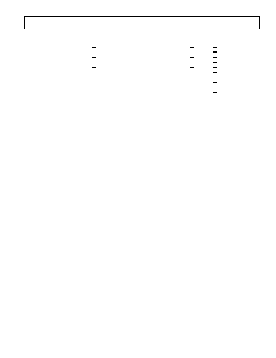
AD5204 PIN FUNCTION DESCRIPTIONS
Pin
No.
Name
Description
1, 2,
12
NC
Not Connected.
3
GND
Ground.
4
CS
Chip Select Input, Active Low. When
CS
returns high, data in the serial input register
is decoded based on the address bits and
loaded into the target RDAC latch.
5
PR
Active low preset to midscale; sets RDAC
registers to 80H.
6
V
DD
Positive power supply, specified for
operation at both +3 V or +5 V. (Sum of
|V
DD
| + |V
SS
| <5.5 V.)
7
SHDN
Active low input. Terminal A open-circuit.
Shutdown controls Variable Resistors #1
through #4.
8
SDI
Serial Data Input. MSB First.
9
CLK
Serial Clock Input, positive edge triggered.
10
SDO
Serial Data Output, Open Drain transistor
requires pull-up resistor.
11
V
SS
Negative Power Supply, specified for
operation at both 0 V or ≠2.7 V. (Sum of
|V
DD
| + |V
SS
| <5.5 V.)
13
B3
B Terminal RDAC #3.
14
W3
Wiper RDAC #3, addr = 010
2
.
15
A3
A Terminal RDAC #3.
16
B1
B Terminal RDAC #1.
17
W1
Wiper RDAC #1, addr = 000
2
.
18
A1
A Terminal RDAC #1.
19
A2
A Terminal RDAC #2.
20
W2
Wiper RDAC #2, addr = 001
2
.
21
B2
B Terminal RDAC #2.
22
A4
A Terminal RDAC #4.
23
W4
Wiper RDAC #4, addr = 011
2
.
24
B4
B Terminal RDAC #4.
AD5206 PIN FUNCTION DESCRIPTIONS
Pin
No.
Name
Description
1
A6
A Terminal RDAC #6.
2
W6
Wiper RDAC #6, addr = 101
2
.
3
B6
B Terminal RDAC #6.
4
GND
Ground.
5
CS
Chip Select Input, Active Low. When
CS
returns high, data in the serial input register
is decoded based on the address bits and
loaded into the target RDAC latch.
6
V
DD
Positive power supply, specified for
operation at both +3 V or +5 V. (Sum of
|V
DD
| + |V
SS
| <5.5 V.)
7
SDI
Serial Data Input. MSB First.
8
CLK
Serial Clock Input, positive edge triggered.
9
V
SS
Negative Power Supply, specified for
operation at both 0 V or ≠2.7 V. (Sum of
|V
DD
| + |V
SS
| <5.5 V.)
10
B5
B Terminal RDAC #5.
11
W5
Wiper RDAC #5, addr = 100
2
.
12
A5
A Terminal RDAC #5.
13
B3
B Terminal RDAC #3.
14
W3
Wiper RDAC #3, addr = 010
2
.
15
A3
A Terminal RDAC #3.
16
B1
B Terminal RDAC #1.
17
W1
Wiper RDAC #1, addr = 000
2
.
18
A1
A Terminal RDAC #1.
19
A2
A Terminal RDAC #2.
20
W2
Wiper RDAC #2, addr = 001
2
.
21
B2
B Terminal RDAC #2.
22
A4
A Terminal RDAC #4.
23
W4
Wiper RDAC #4, addr = 011
2
.
24
B4
B Terminal RDAC #4.
AD5206 PIN CONFIGURATION
24
23
22
21
20
19
18
17
16
15
14
13
1
2
3
4
5
6
7
8
9
10
11
12
A5
W5
B5
V
SS
CLK
A6
W6
B6
GND
SDI
V
DD
CS
B3
W3
A3
B1
W1
B4
W4
A4
B2
A1
A2
W2
AD5206
(NOT TO
SCALE)
AD5204 PIN CONFIGURATION
24
23
22
21
20
19
18
17
16
15
14
13
1
2
3
4
5
6
7
8
9
10
11
12
NC
V
SS
SDO
CLK
SDI
NC
NC
GND
CS
SHDN
V
DD
PR
B3
W3
A3
B1
W1
B4
W4
A4
B2
A1
A2
W2
AD5204
(NOT TO
SCALE)
NC = NO CONNECT
AD5204/AD5206
≠6≠
REV. 0
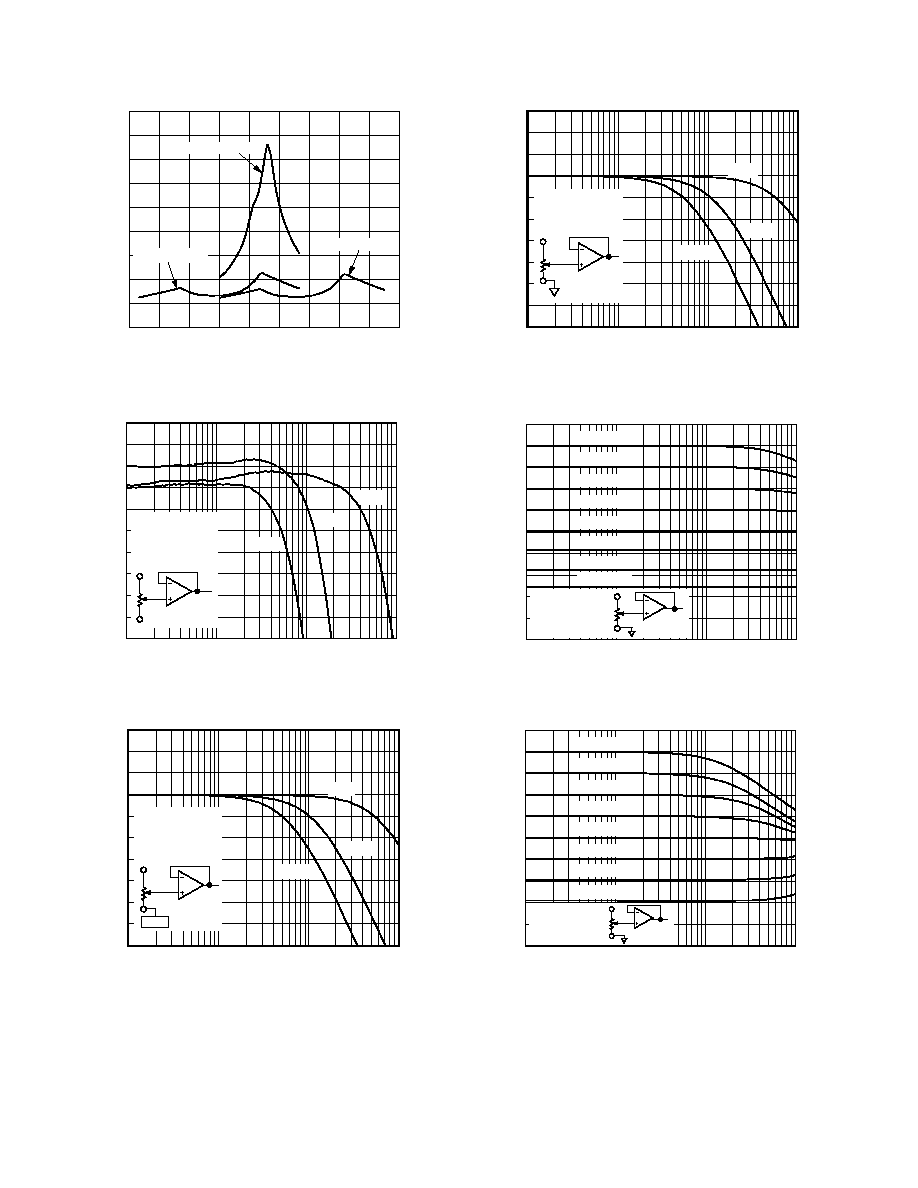
≠Typical Performance Characteristics
COMMON MODE ≠ V
≠3.0
6.0
≠2.0
≠1.0
0
1.0
2.0
3.0
4.0
5.0
120
110
30
SWITCH RESISTANCE ≠
70
60
50
40
90
80
100
V
DD
/V
SS
= 2.7V/0V
V
DD
/V
SS
= 5.5V/0V
V
DD
/V
SS
= 2.7V
Figure 4. Incremental Wiper ON Resistance vs. Voltage
FREQUENCY ≠ Hz
≠5.99
≠6.09
100
100k
GAIN ≠ dB
≠6.08
10k
1k
50k
100k
10k
≠6.07
≠6.06
≠6.05
≠6.04
≠6.03
≠6.02
≠6.01
≠6.00
V
A
OP42
V
B
= 0V
V
DD
= 2.7V
V
SS
= ≠2.7V
V
A
= 100mV rms
DATA = 80
H
T
A
= +25 C
Figure 5. Gain Flatness vs. Frequency
FREQUENCY ≠ Hz
1k
1M
NORMALIZED GAIN ≠ dB
100k
10k
50k
100k
10k
≠4
≠2
0
OP42
+1.5V
2.7V
V
DD
= 2.7V
V
SS
= 0V
V
A
= 100mV rms
DATA = 80
H
T
A
= +25 C
Figure 6. ≠3 dB Bandwidth vs. Terminal Resistance,
2.7 V Single Supply Operation
FREQUENCY ≠ Hz
1k
1M
NORMALIZED GAIN ≠ dB
100k
10k
50k
100k
10k
≠4
≠2
0
OP42
V
A
V
DD
= 2.7V
V
SS
= ≠2.7V
V
A
= 100mV rms
DATA = 80
H
Figure 7. ≠3 dB Bandwidth vs. Terminal Resistance,
±
2.7 V Dual Supply Operation
FREQUENCY ≠ Hz
0
≠60
1k
1M
GAIN ≠ dB
≠54
100k
10k
≠48
≠42
≠36
≠30
≠24
≠18
≠12
≠6
V
DD
= 2.7V
V
SS
= ≠2.7V
V
A
= 100mV rms
T
A
= +25 C
V
A
OP42
DATA = 80
H
DATA = 40
H
DATA = 20
H
DATA = 10
H
DATA = 08
H
DATA = 04
H
DATA = 02
H
DATA = 01
H
Figure 8. Bandwidth vs. Code, 10K Version
FREQUENCY ≠ Hz
0
≠60
1k
1M
GAIN ≠ dB
≠54
100k
10k
≠48
≠42
≠36
≠30
≠24
≠18
≠12
≠6
V
DD
= 2.7V
V
SS
= ≠2.7V
V
A
= 100mV rms
T
A
= +25 C
V
A
OP42
DATA = 80
H
DATA = 40
H
DATA = 20
H
DATA = 10
H
DATA = 08
H
DATA = 04
H
DATA = 02
H
DATA = 01
H
Figure 9. Bandwidth vs. Code, 50K Version
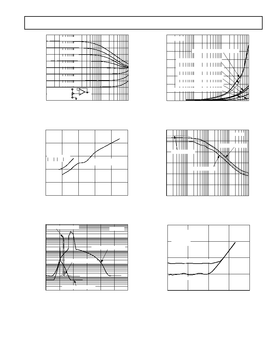
AD5204/AD5206
≠7≠
REV. 0
FREQUENCY ≠ Hz
0
≠60
1k
1M
GAIN ≠ dB
≠54
100k
10k
≠48
≠42
≠36
≠30
≠24
≠18
≠12
≠6
V
DD
= 2.7V
V
SS
= ≠2.7V
V
A
= 100mV rms
T
A
= +25 C
V
A
OP42
DATA = 80
H
DATA = 40
H
DATA = 20
H
DATA = 10
H
DATA = 08
H
DATA = 04
H
DATA = 02
H
DATA = 01
H
Figure 10. Bandwidth vs. Code, 100K Version
SUPPLY VOLTAGE V
DD
≠ Volts
2.5
2.0
0.0
1.0
6.0
2.0
TRIP POINT ≠ V
3.0
4.0
5.0
1.0
0.1
0.5
DUAL SUPPLY
V
SS
= 0V
SINGLE SUPPLY
V
DD
= V
SS
Figure 11. Digital Input Trip Point vs. Supply Voltage
INCREMENTAL INPUT LOGIC VOLTAGE ≠ Volts
100
0.001
0
5
SUPPLY CURRENT ≠ mA
10
1
2
3
4
6
1
0.1
0.01
T
A
= +25 C
I
DD
AT V
DD
/V
SS
= 2.7V/0V
I
DD
AT V
DD
/V
SS
= 5.5V/0V
I
SS
AT V
DD
/V
SS
= 2.7V
I
DD
AT V
DD
/V
SS
= 2.7V
Figure 12. Supply Current vs. Input Logic Voltage
8
0
10k
10M
SUPPLY CURRENT ≠ mA
7
1M
100k
FREQUENCY ≠ Hz
I
DD
, V
DD
/V
SS
= 5.5V/0V, DATA = 55H
I
SS
, V
DD
/V
SS
= 2.7V, DATA = 55H
I
SS
, V
DD
/V
SS
= 2.7V, DATA = FFH
I
DD
, V
DD
/V
SS
= 5,5V/0V, DATA = FFH
I
DD
, V
DD
/V
SS
= 2.7V/0V, DATA = FFH
I
DD
, V
DD
/V
SS
= 2.7V/0V, DATA = 55H
6
5
4
3
2
1
T
A
= +25 C
Figure 13. Supply Current vs. Clock Frequency
0
10
100k
PSRR ≠ dB
10k
100
FREQUENCY ≠ Hz
T
A
= +25 C
V
DD
= 5.0V 10%
V
DD
= 3.0V 10%
V
SS
= ≠3.0V 10%
60
50
40
30
20
10
1k
Figure 14. Power Supply Rejection vs. Frequency
FREQUENCY ≠ Hz
10
THD + NOISE ≠ %
1.0
V
DD
= +2.7V
V
SS
= ≠2.7V
T
A
= +25 C
R
AB
= 10k
NONINVERTING TEST CIRCUIT
INVERTING TEST CIRCUIT
100
1k
10k
100k
0.0001
0.001
0.01
0.1
Figure 15. Total Harmonic Distortion Plus Noise vs.
Frequency

AD5204/AD5206
≠8≠
REV. 0
OPERATION
The AD5204/AD5206 provides a four-/six-channel, 256-position
digitally-controlled variable resistor (VR) device. Changing the
programmed VR settings is accomplished by clocking in a 11-
bit serial data word into the SDI (Serial Data Input) pin. The
format of this data word is three address bits, MSB first, fol-
lowed by eight data bits, MSB first. Table I provides the serial
register data word format.
Table I. Serial-Data Word Format
ADDR
DATA
B10 B9
B8
B7
B6
B5
B4
B3
B2
B1
B0
A2
A1
A0
D7
D6
D5
D4
D3
D2
D1
D0
MSB
LSB
MSB
LSB
2
10
2
8
2
7
2
0
See Table IV for the AD5204/AD5206 address assignments to
decode the location of VR latch receiving the serial register data
in Bits B7 through B0. VR outputs can be changed one at a
time in random sequence. The AD5204 presets to a midscale by
asserting the PR pin, simplifying fault condition recovery at
power up. Both parts have an internal power ON preset that
places the wiper in a preset midscale condition at power ON. In
addition, the AD5204 contains a power shutdown SHDN pin
which places the RDAC in a zero power consumption state
where Terminals Ax are open circuited and the wiper Wx is
connected to Bx resulting in only leakage currents being con-
sumed in the VR structure. In shutdown mode the VR latch
settings are maintained, so that, returning to operational mode
from power shutdown, the VR settings return to their previous
resistance values.
Ax
Wx
Bx
R
S
R
S
R
S
R
S
SHDN
D7
D6
D5
D4
D3
D2
D1
D0
RDAC
LATCH
&
DECODER
Figure 16. AD5204/AD5206 Equivalent RDAC Circuit
PROGRAMMING THE VARIABLE RESISTOR
Rheostat Operation
The nominal resistance of the RDAC between Terminals A and
B are available with values of 10 k
, 50 k
and 100 k
. The
last digits of the part number determine the nominal resistance
value, e.g., 10 k
= 10; 100 k
= 100. The nominal resistance
(R
AB
) of the VR has 256 contact points accessed by the wiper
terminal, plus the B terminal contact. The eight-bit data word
in the RDAC latch is decoded to select one of the 256 possible
settings. The wiper's first connection starts at the B terminal for
data 00
H
. This B terminal connection has a wiper contact resis-
tance of 45
. The second connection (10 k
part) is the first
tap point located at 84
[= R
BA
(nominal resistance)/256 + R
W
= 84
+ 45
] for data 01
H
. The third connection is the next
tap point representing 78 + 45 = 123
for data 02
H
. Each LSB
data value increase moves the wiper up the resistor ladder until
the last tap point is reached at 10006
. The wiper does not
directly connect to the A terminal. See Figure 16 for a simplified
diagram of the equivalent RDAC circuit.
The general transfer equation determining the digitally pro-
grammed output resistance between Wx and Bx is:
R
WB
(Dx) = (Dx)/256
◊
R
BA
+ R
W
(1)
where Dx is the data contained in the 8-bit RDACx latch, and
R
BA
is the nominal end-to-end resistance.
For example, when V
B
= 0 V and A terminal is open-circuit, the
following output resistance values will be set for the following
RDAC latch codes (applies to the 10K potentiometer):
Table II.
D
(DEC)
R
WB
-
Output State
255
10006
Full Scale
128
5045
Midscale (
PR = 0 Condition)
1
84
1 LSB
0
45
Zero Scale (Wiper Contact Resistance)
Note that in the zero-scale condition a finite wiper resistance of
45
is present. Care should be taken to limit the current flow
between W and B in this state to a maximum value of 20 mA to
avoid degradation or possible destruction of the internal switch
contact.
Like the mechanical potentiometer the RDAC replaces, it is
totally symmetrical. The resistance between the Wiper W and
Terminal A produces a digitally controlled resistance R
WA
.
When these terminals are used the B terminal should be tied to
the wiper. Setting the resistance value for R
WA
starts at a maxi-
mum value of resistance and decreases as the data loaded in the
latch is increased in value. The general transfer equation for this
operation is:
R
WA
(Dx) = (256≠Dx)/256
◊
R
BA
+ R
W
(2)
where Dx is the data contained in the 8-bit RDACx latch, and
R
BA
is the nominal end-to-end resistance. For example, when
V
A
= 0 V and B terminal is tied to the Wiper W the following
output resistance values will be set for the following RDAC
latch codes:
Table III.
D
(DEC)
R
WA
-
Output State
255
84
Full Scale
128
5045
Midscale (
PR = 0 Condition)
1
10006
1 LSB
0
10045
Zero Scale
AD5204/AD5206
≠9≠
REV. 0
The typical distribution of R
BA
from channel-to-channel matches
within
±
1%. However, device-to-device matching is process lot
dependent, having a
±
30% variation. The change in R
BA
with
temperature has a 700 ppm/
∞
C temperature coefficient.
PROGRAMMING THE POTENTIOMETER DIVIDER
Voltage Output Operation
The digital potentiometer easily generates an output voltage
proportional to the input voltage applied to a given terminal.
For example, connecting A terminal to +5 V and B terminal to
ground produces an output voltage at the wiper which can be
any value starting at zero volts up to 1 LSB less than +5 V. Each
LSB of voltage is equal to the voltage applied across Terminal
AB divided by the 256-position resolution of the potentiometer
divider. The general equation defining the output voltage with
respect to ground for any given input voltage applied to termi-
nals AB is:
V
W
(Dx) = Dx/256
◊
V
AB
+ V
B
(3)
Operation of the digital potentiometer in the divider mode results
in more accurate operation over temperature. Here the output
voltage is dependent on the ratio of the internal resistors not the
absolute value, therefore, the drift improves to 15 ppm/
∞
C.
D7
D0
A1
W1
B1
V
DD
AD5204/AD5206
CS
CLK
8
EN
ADDR
DEC
A2
A1
A0
SDI
DI
SER
REG
D0
D7
A4/A6
W4/W6
B4/B6
SHDN
RDAC
LATCH
#1
R
D7
D0
RDAC
LATCH
#4/#6
R
SDO
DO
GND
PR
(AD5204 ONLY)
(AD5204
ONLY)
(AD5204
ONLY)
Figure 17. Block Diagram
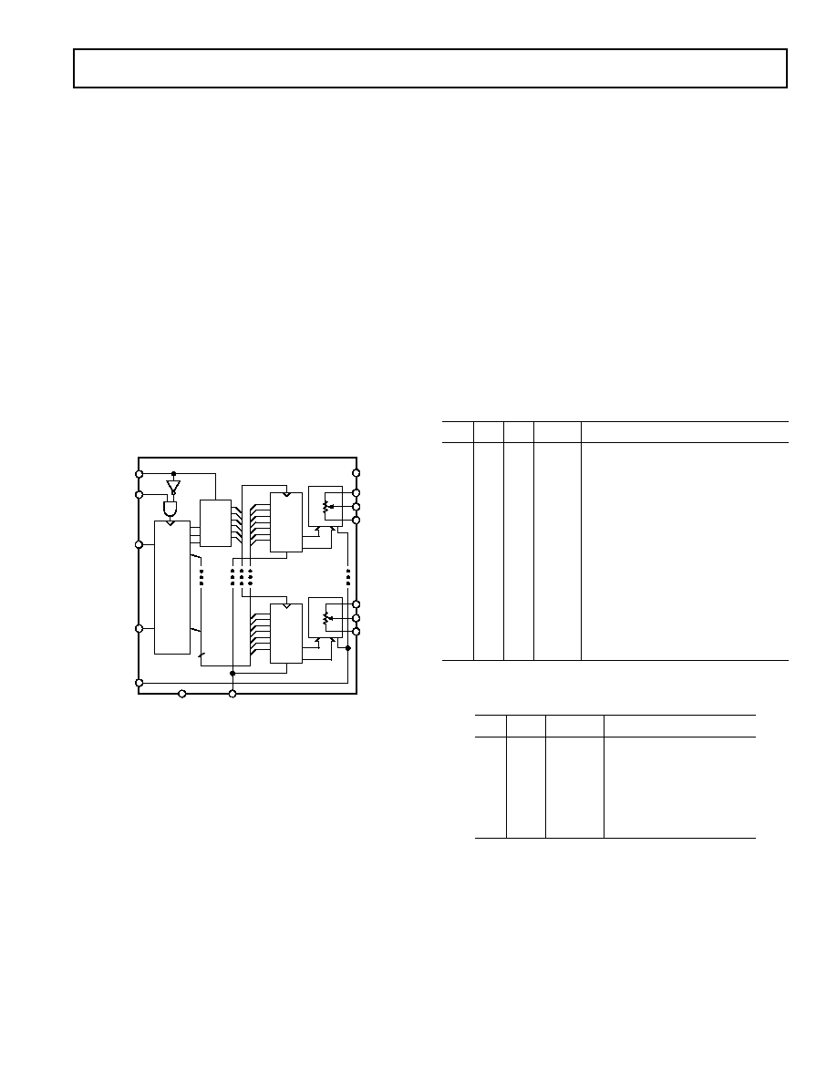
DIGITAL INTERFACING
The AD5204/AD5206 contain a standard three-wire serial input
control interface. The three inputs are clock (CLK),
CS and
serial data input (SDI). The positive-edge sensitive CLK input
requires clean transitions to avoid clocking incorrect data into
the serial input register. Standard logic families work well. If
mechanical switches are used for product evaluation they should
be debounced by a flip-flop or other suitable means. Figure 17
shows more detail of the internal digital circuitry. When
CS is
taken active low the clock loads data into the serial register on
each positive clock edge, see Table IV. When using a positive
(V
DD
) and negative (V
SS
) supply voltage, the logic levels are still
referenced to digital ground (GND).
The serial-data-output (SDO) pin contains an open drain n-
channel FET. This output requires a pull-up resistor in order to
transfer data to the next package's SDI pin. The pull-up resistor
termination voltage may be larger than the V
DD
supply of the
AD5204 SDO output device, e.g., the AD5204 could operate at
V
DD
= 3.3 V and the pull-up for interface to the next device
could be set at +5 V. This allows for daisy chaining several
RDACs from a single processor serial-data line. Clock period
needs to be increased when using a pull-up resistor to the SDI
pin of the following device in the series. Capacitive loading at
the daisy chain node SDO-SDI between devices must be ac-
counted for to successfully transfer data. When daisy chaining is
used, the
CS should be kept low until all the bits of every pack-
age are clocked into their respective serial registers insuring that
the address bits and data bits are in the proper decoding loca-
tion. This would require 22 bits of address and data complying
to the word format provided in Table I if two AD5204 four-
channel RDACs are daisy chained. During shutdown
(SHDN)
the SDO output pin is forced to the off (logic high state) to
disable power dissipation in the pull-up resistor. See Figure 19
for equivalent SDO output circuit schematic.
Table IV. Input Logic Control Truth Table
CLK
CS PR SHDN Register Activity
L
L
H
H
No SR effect, enables SDO pin.
P
L
H
H
Shift one bit in from the SDI pin.
The eleventh previously entered bit
is shifted out of the SDO pin.
X
P
H
H
Load SR data into RDAC latch based
on A2, A1, A0 decode (Table V).
X
H
H
H
No Operation.
X
X
L
H
Sets all RDAC latches to midscale,
wiper centered and SDO latch
cleared.
X
H
P
H
Latches all RDAC latches to 80
H
.
X
H
H
L
Open circuits all Resistor A termi-
nals, connects W to B, turns off
SDO output transistor.
NOTE: P = positive edge, X = don't care, SR = shift register.
Table V. Address Decode Table
A2
A1
A0
Latch Decoded
0
0
0
RDAC#1
0
0
1
RDAC#2
0
1
0
RDAC#3
0
1
1
RDAC#4
1
0
0
RDAC#5 AD5206 Only
1
0
1
RDAC#6 AD5206 Only
The data setup and data hold times in the specification table
determine the data valid time requirements. The last 11 bits of
the data word entered into the serial register are held when
CS
returns high. At the same time
CS goes high it gates the address
decoder enabling one of four or six positive edge triggered RDAC
latches, see Figure 18 detail.

AD5204/AD5206
≠10≠
REV. 0
RDAC 1
RDAC 2
RDAC 4/6
AD5204/AD5206
SDI
CLK
CS
ADDR
DECODE
SERIAL
REGISTER
Figure 18. Equivalent Input Control Logic
The target RDAC latch is loaded with the last eight bits of the
serial data word completing one DAC update. Four separate 8-
bit data words must be clocked in to change all four VR settings.
SERIAL
REGISTER
SDI
CK
RS
D
Q
SHDN
CS
CLK
PR
SDO
GND
Figure 19. Detail SDO Output Schematic of the AD5204
All digital pins are protected with a series input resistor and
parallel Zener ESD structure shown in Figure 20. Applies to
digital pins
CS, SDI, SDO, PR, SHDN, CLK
340k
LOGIC
V
SS
Figure 20. ESD Protection of Digital Pins
A, B, W
V
SS
Figure 21. ESD Protection of Resistor Terminals
V+
DUT
V
MS
A
B
W
V+ = V
DD
1LSB = V+/256
Figure 22. Potentiometer Divider Nonlinearity Error Test
Circuit (INL, DNL)
NO CONNECT
I
W
DUT
V
MS
A
B
W
Figure 23. Resistor Position Nonlinearity Error (Rheostat
Operation; R-INL, R-DNL)
I
MS
V
W
I
W
=
1V/R
NOMINAL
DUT
V
MS
A
B
W
V+
I
W
R
W
= ≠≠≠≠≠≠≠≠≠≠≠≠≠≠≠≠≠≠≠≠≠≠≠≠≠≠
V
W 2
≠[V
W1
+ I
W
(R
AW
II R
BW
)]
WHERE V
W1
= V
MS
WHEN I
W
= 0
AND V
W2
= V
MS
WHEN I
W
= 1/R
V+
V
DD
Figure 24. Wiper Resistance Test Circuit
PSRR (dB) = 20 LOG
(
≠≠≠≠≠
)
PSS (%/%) = ≠≠≠≠≠≠≠
V
MS
V
DD
V
MS
%
V
DD
%
V+ = V
DD
± 10%
V
DD
V
A
~
V+
V
MS
A
B
W
Figure 25. Power Supply Sensitivity Test Circuit (PSS,
PSRR)
A
B
V
IN
OP279
+5V
V
OUT
DUT
W
OFFSET
GND
+
OFFSET BIAS
Figure 26. Inverting Programmable Gain Test Circuit
A
B
V
IN
OP279
+5V
V
OUT
DUT
W
OFFSET
GND
OFFSET BIAS
Figure 27. Noninverting Programmable Gain Test Circuit
+15V
≠15V
A
B
V
IN
2.5V
OP42
V
OUT
DUT
W
OFFSET
GND
+
Figure 28. Gain vs. Frequency Test Circuit
I
SW
V
SS
TO V
DD
R
SW
=
0.1V
I
SW
CODE = ÿÿ
H
0.1V
DUT
B
W
+
Figure 29. Incremental ON Resistance Test Circuit

AD5204/AD5206
≠11≠
REV. 0
24-Lead Narrow Body PDIP
(N-24)
24
1
12
13
PIN 1
1.275 (32.30)
1.125 (28.60)
0.280 (7.11)
0.240 (6.10)
0.195 (4.95)
0.115 (2.93)
0.015 (0.381)
0.008 (0.204)
0.325 (8.25)
0.300 (7.62)
SEATING
PLANE
0.060 (1.52)
0.015 (0.38)
0.210
(5.33)
MAX
0.022 (0.558)
0.014 (0.356)
0.200 (5.05)
0.125 (3.18)
0.150
(3.81)
MIN
0.100
(2.54)
BSC
0.070 (1.77)
0.045 (1.15)
24-Lead SOIC
(R-24/SOL-24)
0.0125 (0.32)
0.0091 (0.23)
8
0
0.0291 (0.74)
0.0098 (0.25)
45
0.0500 (1.27)
0.0157 (0.40)
SEATING
PLANE
0.0118 (0.30)
0.0040 (0.10)
0.0192 (0.49)
0.0138 (0.35)
0.1043 (2.65)
0.0926 (2.35)
0.0500
(1.27)
BSC
24
13
12
1
0.4193 (10.65)
0.3937 (10.00)
0.2992 (7.60)
0.2914 (7.40)
PIN 1
0.6141 (15.60)
0.5985 (15.20)
24-Lead Thin Shrink SO Package (TSSOP)
(RU-24)
24
13
12
1
0.256 (6.50)
0.246 (6.25)
0.177 (4.50)
0.169 (4.30)
PIN 1
0.311 (7.90)
0.303 (7.70)
SEATING
PLANE
0.006 (0.15)
0.002 (0.05)
0.0118 (0.30)
0.0075 (0.19)
0.0256 (0.65)
BSC
0.0433 (1.10)
MAX
0.0079 (0.20)
0.0035 (0.090)
0.028 (0.70)
0.020 (0.50)
8
0
OUTLINE DIMENSIONS
Dimensions shown in inches and (mm).
C3677≠8≠9/99
PRINTED IN U.S.A.