Äîêóìåíòàöèÿ è îïèñàíèÿ www.docs.chipfind.ru
REV. 0
Information furnished by Analog Devices is believed to be accurate and
reliable. However, no responsibility is assumed by Analog Devices for its
use, nor for any infringements of patents or other rights of third parties
which may result from its use. No license is granted by implication or
otherwise under any patent or patent rights of Analog Devices.
a
AD5220
One Technology Way, P.O. Box 9106, Norwood, MA 02062-9106, U.S.A.
Tel: 781/329-4700
World Wide Web Site: http://www.analog.com
Fax: 781/326-8703
© Analog Devices, Inc., 1998
Increment/Decrement
Digital Potentiometer
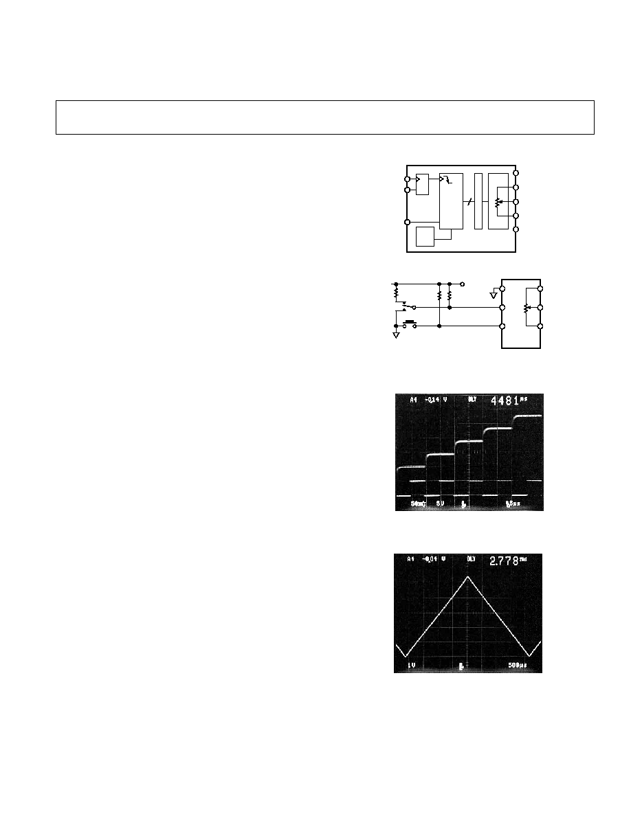
FUNCTIONAL BLOCK DIAGRAM
UP/
DOWN
CNTR
RS
D
E
C
O
D
E
7
40
H
POR
EN
AD5220
V
DD
A
W
B
GND
CLK
CS
U/
D
FEATURES
128 Position
Potentiometer Replacement
10 k , 50 k , 100 k
Very Low Power: 40 A Max
Increment/Decrement Count Control
APPLICATIONS
Mechanical Potentiometer Replacement
Remote Incremental Adjustment Applications
Instrumentation: Gain, Offset Adjustment
Programmable Voltage-to-Current Conversion
Programmable Filters, Delays, Time Constants
Line Impedance Matching
Power Supply Adjustment
GENERAL DESCRIPTION
The AD5220 provides a single channel, 128-position digitally
controlled variable resistor (VR) device. This device performs
the same electronic adjustment function as a potentiometer or
variable resistor. These products were optimized for instrument
and test equipment push-button applications. A choice between
bandwidth or power dissipation are available as a result of the
wide selection of end-to-end terminal resistance values.
The AD5220 contains a fixed resistor with a wiper contact that
taps the fixed resistor value at a point determined by a digitally
controlled UP/DOWN counter. The resistance between the
wiper and either end point of the fixed resistor provides a con-
stant resistance step size that is equal to the end-to-end resis-
tance divided by the number of positions (e.g., R
STEP
= 10 k
/
128 = 78
). The variable resistor offers a true adjustable value
of resistance, between the A terminal and the wiper, or the B
terminal and the wiper. The fixed A-to-B terminal resistance of
10 k
, 50 k
, or 100 k
has a nominal temperature coefficient
of 800 ppm/
°
C.
The chip select CS, count CLK and U/D direction control
inputs set the variable resistor position. These inputs that con-
trol the internal UP/DOWN counter can be easily generated
with mechanical or push button switches (or other contact closure
devices). External debounce circuitry is required for the nega-
tive-edge sensitive CLK pin. This simple digital interface elimi-
nates the need for microcontrollers in front panel interface designs.
The AD5220 is available in both surface mount (SO-8) and the
8-lead plastic DIP package. For ultracompact solutions selected
models are available in the thin
µ
SOIC package. All parts are
guaranteed to operate over the extended industrial temperature
range of 40
°
C to +85
°
C. For 3-wire, SPI compatible inter-
face applications, see the AD7376/AD8400/AD8402/AD8403
products.
UPCOUNT DETAIL
V
DD
= 5.5V
V
A
= 5.5V
V
B
= 0V
f = 100kHz
CLK
V
WB
50mV/DIV
5V/DIV
Figure 2a. Stair-Step Increment Output
V
DD
= 5.5V
V
A
= 5.5V
V
B
= 0V
f = 60kHz
COUNT
00
H
v
3F
H
v
00
H
V
WR
f
CLK
= 60kHz
Figure 2b. Full-Scale Up/Down Count
AD5220
CS
U/
D
CLK
+5V
UP/DOWN
INCREMENT
Figure 1. Typical Push-Button Control Application

2
REV. 0
AD5220SPECIFICATIONS
ELECTRICAL CHARACTERISTICS
Parameter
Symbol
Conditions
Min
Typ
1
Max
Units
DC CHARACTERISTICS RHEOSTAT MODE Specifications Apply to All VRs
Resistor Differential NL
2
R-DNL
R
WB
, V
A
= NC, R
AB
= 10 k
1
±
0.4
+1
LSB
R
WB
, V
A
= NC, R
AB
= 50 k
or 100 k
0.5
±
0.1
+0.5
LSB
Resistor Nonlinearity
2
R-INL
R
WB
, V
A
= NC, R
AB
= 10 k
1
±
0.5
+1
LSB
R
WB
, V
A
= NC, R
AB
= 50 k
or 100 k
0.5
±
0.1
+0.5
LSB
Nominal Resistor Tolerance
R
T
A
= +25
°
C
30
+30
%
Resistance Temperature Coefficient
R
AB
/
T
V
AB
= V
DD
, Wiper = No Connect
800
ppm/
°
C
Wiper Resistance
R
W
I
W
= V
DD
/R, V
DD
= +3 V or +5 V
40
100
DC CHARACTERISTICS POTENTIOMETER DIVIDER MODE Specifications Apply to All VRs
Resolution
N
7
Bits
Integral Nonlinearity
3
INL
R
AB
= 10 k
1
±
0.5
+1
LSB
R
AB
= 50 k
, 100 k
0.5
±
0.2
+0.5
LSB
Differential Nonlinearity Error
3
DNL
R
AB
= 10 k
1
±
0.4
+1
LSB
R
AB
= 50 k
, 100 k
0.5
±
0.1
+0.5
LSB
Voltage Divider Temperature Coefficient
V
W
/
T
Code = 40
H
20
ppm/
°
C
Full-Scale Error
V
WFSE
Code = 7F
H
2
0.5
0
LSB
Zero-Scale Error
V
WZSE
Code = 00
H
0
+0.5
+1
LSB
RESISTOR TERMINALS
Voltage Range
4
V
A,
V
B,
V
W
0
V
DD
V
Capacitance
5
A, B
C
A,
C
B
f = 1 MHz, Measured to GND, Code = 40
H
10
pF
Capacitance
5
W
C
W
f = 1 MHz, Measured to GND, Code = 40
H
48
pF
Common-Mode Leakage
I
CM
V
A
= V
B
= V
W
7.5
nA
DIGITAL INPUTS AND OUTPUTS
Input Logic High
V
IH
V
DD
= +5 V/+3 V
2.4/2.1
V
Input Logic Low
V
IL
V
DD
= +5 V/+3 V
0.8/0.6
V
Input Current
I
IL
V
IN
= 0 V or +5 V
±
1
µ
A
Input Capacitance
5
C
IL
5
pF
POWER SUPPLIES
Power Supply Range
V
DD
2.7
5.5
V
Supply Current
I
DD
V
IH
= +5 V or V
IL
= 0 V, V
DD
= +5 V
15
40
µ
A
Power Dissipation
6
P
DISS
V
IH
= +5 V or V
IL
= 0 V, V
DD
= +5 V
75
200
µ
W
Power Supply Sensitivity
PSS
0.004
0.015
%/%
DYNAMIC CHARACTERISTICS
5, 7, 8
Bandwidth 3 dB
BW_10K
R
AB
= 10 k
, Code = 40
H
650
kHz
BW_50K
R
AB
= 50 k
, Code = 40
H
142
kHz
BW_100K
R
AB
= 100 k
, Code = 40
H
69
kHz
Total Harmonic Distortion
THD
W
V
A
=1 V rms + 2.5 V dc, V
B
= 2.5 V dc, f = 1 kHz
0.002
%
V
W
Settling Time
t
S
V
A
= V
DD
, V
B
= 0 V, 50% of Final Value,
10K/50K/100K
0.6/3/6
µ
s
Resistor Noise Voltage
e
NWB
R
WB
= 5 k
, f = 1 kHz
14
nV/
Hz
INTERFACE TIMING CHARACTERISTICS Applies to All Parts
5, 9
Input Clock Pulsewidth
t
CH
, t
CL
Clock Level High or Low
25
ns
CS to CLK Setup Time
t
CSS
20
ns
CS Rise to Clock Hold Time
t
CSH
20
ns
U/D to Clock Fall Setup Time
t
UDS
10
ns
NOTES
1
Typicals represent average readings at +25
°
C and V
DD
= +5 V.
2
Resistor position nonlinearity error R-INL is the deviation from an ideal value measured between the maximum resistance and the minimum resistance wiper
positions. R-DNL measures the relative step change from ideal between successive tap positions. Parts are guaranteed monotonic. See Figure 29 test circuit.
3
INL and DNL are measured at V
W
with the RDAC configured as a potentiometer divider similar to a voltage output D/A converter. V
A
= V
DD
and V
B
= 0 V.
DNL specification limits of
±
1 LSB maximum are guaranteed monotonic operating conditions. See Figure 28 test circuit.
4
Resistor terminals A, B, W have no limitations on polarity with respect to each other.
5
Guaranteed by design and not subject to production test.
6
P
DISS
is calculated from (I
DD
×
V
DD
). CMOS logic level inputs result in minimum power dissipation.
7
Bandwidth, noise and settling time are dependent on the terminal resistance value chosen. The lowest R value results in the fastest settling time and highest band-
width. The highest R value results in the minimum overall power consumption.
8
All dynamic characteristics use V
DD
= +5 V.
9
See timing diagrams for location of measured values. All input control voltages are specified with t
R
= t
F
= 1 ns (10% to 90% of V
DD
) and timed from a voltage level
of 1.6 V. Switching characteristics are measured using both V
DD
= +3 V or +5 V.
Specifications subject to change without notice.
(V
DD
= +3 V 10% or +5 V 10%, V
A
= +V
DD
, V
B
= 0 V, 40 C < T
A
< +85 C unless
otherwise noted)
AD5220
3
REV. 0
ABSOLUTE MAXIMUM RATINGS*
(T
A
= +25
°
C, unless otherwise noted)
V
DD
to GND . . . . . . . . . . . . . . . . . . . . . . . . . . . . 0.3 V, +7 V
V
A
, V
B
, V
W
to GND . . . . . . . . . . . . . . . . . . . . . . . . . . 0 V, V
DD
A
X
B
X
, A
X
W
X
, B
X
W
X
. . . . . . . . . . . . . . . . . . . . . .
±
20 mA
Digital Input Voltage to GND . . . . . . . . . . . 0 V, V
DD
+ 0.3 V
Operating Temperature Range . . . . . . . . . . . 40
°
C to +85
°
C
Maximum Junction Temperature (T
J
MAX) . . . . . . . . +150
°
C
Storage Temperature . . . . . . . . . . . . . . . . . . 65
°
C to +150
°
C
Lead Temperature (Soldering, 10 sec) . . . . . . . . . . . . +300
°
C
Package Power Dissipation . . . . . . . . . . . . . . (T
J
maxT
A
)/
JA
Thermal Resistance
JA
P-DIP (N-8) . . . . . . . . . . . . . . . . . . . . . . . . . . . . 103
°
C/W
SOIC (SO-8) . . . . . . . . . . . . . . . . . . . . . . . . . . . . 158
°
C/W
µ
SOIC (RM-8) . . . . . . . . . . . . . . . . . . . . . . . . . . . 206
°
C/W
*Stresses above those listed under Absolute Maximum Ratings may cause
permanent damage to the device. This is a stress rating only; functional operation
of the device at these or any other conditions above those indicated in the
operational sections of this specification is not implied. Exposure to absolute
maximum rating conditions for extended periods may affect device reliability.
CAUTION
ESD (electrostatic discharge) sensitive device. Electrostatic charges as high as 4000 V readily
accumulate on the human body and test equipment and can discharge without detection.
Although the AD5220 features proprietary ESD protection circuitry, permanent damage may
occur on devices subjected to high energy electrostatic discharges. Therefore, proper ESD
precautions are recommended to avoid performance degradation or loss of functionality.
WARNING!
ESD SENSITIVE DEVICE
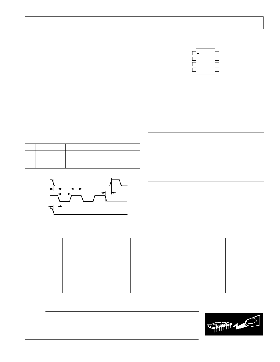
PIN CONFIGURATION
TOP VIEW
(Not to Scale)
8
7
6
5
1
2
3
4
CLK
U/
D
A1
GND
V
DD
CS
B1
W1
AD5220
t
CSS
t
CH
t
CSH
t
UDS
t
CL
1
0
1
0
1
0
CS
CLK
U/
D
Figure 3. Detail Timing Diagram
ORDERING GUIDE
Model
k
Temperature Range
Package Descriptions
Package Options
AD5220BN10
10
40
°
C to +85
°
C
8-Lead Plastic DIP
N-8
AD5220BR10
10
40
°
C to +85
°
C
8-Lead (SOIC)
SO-8
AD5220BRM10
10
40
°
C to +85
°
C
8-Lead
µ
SOIC
RM-8
AD5220BN50
50
40
°
C to +85
°
C
8-Lead Plastic DIP
N-8
AD5220BR50
50
40
°
C to +85
°
C
8-Lead (SOIC)
SO-8
AD5220BRM50
50
40
°
C to +85
°
C
8-Lead
µ
SOIC
RM-8
AD5220BN100
100
40
°
C to +85
°
C
8-Lead Plastic DIP
N-8
AD5220BR100
100
40
°
C to +85
°
C
8-Lead (SOIC)
SO-8
AD5220BRM100
100
40
°
C to +85
°
C
8-Lead
µ
SOIC
RM-8
NOTE
The AD5220 die size is 37 mil
×
54 mil, 1998 sq mil; 0.938 mm
×
1.372 mm, 1.289 sq mm. Contains 754 transistors. Patent Number 5495245 applies.
Table I. Truth Table
CS
CLK
U/D
Operation
L
t
H
Wiper Increment Toward Terminal A
L
t
L
Wiper Decrement Toward Terminal B
H
X
X
Wiper Position Fixed
PIN FUNCTION DESCRIPTIONS
Pin
No.
Name
Description
1
CLK
Serial Clock Input, Negative Edge Triggered
2
U/D
UP/DOWN Direction Increment Control
3
A1
Terminal A1
4
GND
Ground
5
W1
Wiper Terminal
6
B1
Terminal B1
7
CS
Chip Select Input, Active Low
8
V
DD
Positive Power Supply
AD5220
4
REV. 0
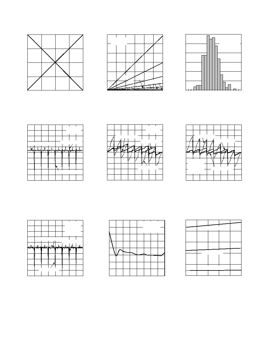
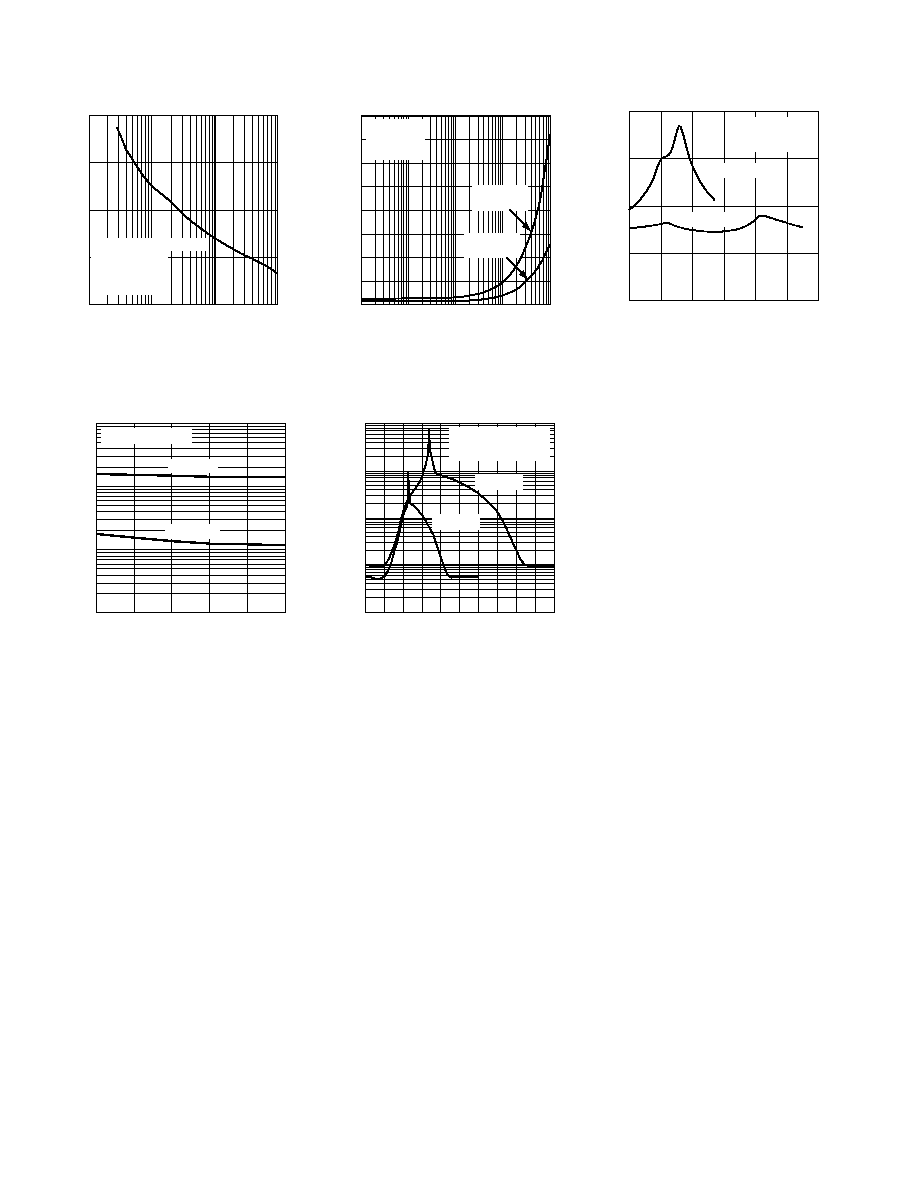
Typical Performance Characteristics
PERCENT OF NOMINAL
END-TO-END RESISTANCE % R
AB
100
75
0
0
32
128
64
96
50
25
R
WB
R
WA
CODE Decimal
Figure 4. Wiper to End Terminal
Resistance vs. Code
CODE Decimal
RDNL LSB
0.5
0.5
0
16
128
32
48
64
80
96
112
0.4
0.1
0.0
0.2
0.4
0.3
0.2
0.1
0.3
T
A
= +25 C
V
DD
= +5.5V
50k
VERSION
10k
VERSION
100k
VERSION
Figure 7. R-DNL Relative Resistance
Step Position Nonlinearity Error vs.
Code
CODE Decimal
DNL LSB
0.5
0.5
0
16
128
32
48
64
80
96
112
0.4
0.1
0.0
0.2
0.4
0.3
0.2
0.1
0.3
50k
VERSION
10k
VERSION
100k
VERSION
T
A
= +25 C
V
DD
= +5.5V
V
A
= +5.5V
V
B
= 0V
Figure 10. Potentiometer Divider
DNL Error vs. Code
CONDUCTION CURRENT, I
WB
A
V
WB
V
6
0
0
20
120
40
60
80
100
5
4
3
2
1
V
DD
= 5.5V
R
AB
= 50k
7F
H
08
H
01
H
02
H
04
H
10
H
20
H
40
H
Figure 5. Resistance Linearity vs.
Conduction Current
CODE Decimal
RINL LSB
0.5
0.5
0
16
128
32
48
64
80
96
112
0.4
0.1
0.0
0.2
0.4
0.3
0.2
0.1
0.3
T
A
= +25 C
V
DD
= +5.5V
50k
VERSION
10k
VERSION
100k
VERSION
Figure 8. R-INL Resistance Non-
linearity Error vs. Supply Voltage
SUPPLY VOLTAGE V
POTENTIOMETER DIVIDER
NONLINEARITY LSB
0.600
0.000
2.00 2.50
6.00
3.00 3.50 4.00 4.50 5.00 5.50
0.525
0.300
0.255
0.150
0.075
0.450
0.375
CODE = 40
H
R
AB
= 50k
V
A
= V
DD
Figure 11. Potentiometer Divider
INL Error vs. Supply Voltage
WIPER RESISTANCE
FREQUENCY
48
24
0
20
40
32
16
8
28
36
44
52
60
SS = 300 UNITS
V
DD
= +2.7V
T
A
= +25 C
Figure 6. Wiper Contact Resistance
CODE Decimal
INL LSB
0.5
0.5
0
16
128
32
48
64
80
96
112
0.4
0.1
0.0
0.2
0.4
0.3
0.2
0.1
0.3
T
A
= +25 C
V
DD
= +5.5V
V
A
= +5.5V
V
B
= 0V
50k
VERSION
10k
VERSION
100k
VERSION
Figure 9. Potentiometer Divider INL
Error vs. Code
TEMPERATURE C
NOMINAL END-TO-END RESISTANCE k
100
80
0
40
15
85
10
35
60
60
40
20
100k
VERSION
50k
VERSION
10k
VERSION
Figure 12. Nominal Resistance vs.
Temperature
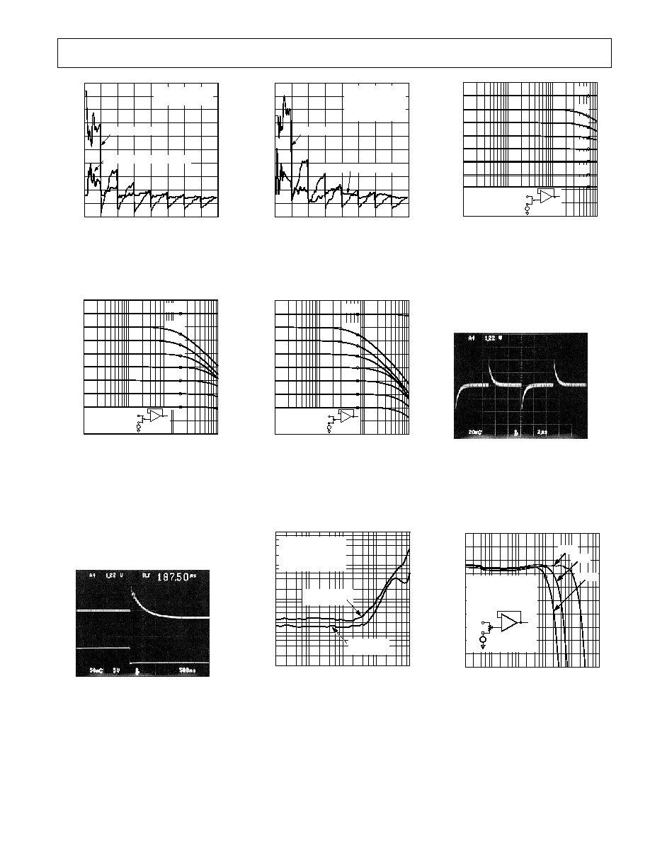
AD5220
5
REV. 0
CODE Decimal
POTENTIOMETER MODE TEMPCO ppm/
C
60
10
0
16
128
32
48
64
80
96
112
53
32
25
11
3
46
39
18
4
55 C < T
A
< +85 C
V
DD
= +5.5V
50k
AND 100k
VERSION
10k
VERSION
Figure 13.
V
WB
/
T Potentiometer
Mode Tempco (10 k
and 50 k
)
FREQUENCY Hz
GAIN dB
6
1k
1M
10k
100k
0
6
12
18
24
30
36
42
48
54
00
H
+
2.5V
W
A
B
OP42
+
DATA = 40
H
V
DD
= +5V
V
IN
= VA = 100mV rms
V
B
= +2.5V
40
H
20
H
10
H
08
H
04
H
02
H
01
H
Figure 16. 50 k
Gain vs. Frequency
vs. Code
V
WB
V
DD
= +5.5V
V
A
= +5.5V
V
B
= 0V
f = 100kHz
DATA
40
H
v
3F
H
150mV
100mV
50mV
0mV
5V
0V
CLK
TIME 500ns / DIV
Figure 19. Midscale Transition Glitch
CODE Decimal
RHEOSTAT MODE TEMPCO ppm/
C
60
10
0
16
128
32
48
64
80
96
112
53
32
25
11
3
46
39
18
4
55 C < T
A
< +85 C
V
DD
= +5.5V
R
WB
MEASURED
V
A
= NO CONNECT
50k
AND 100k
VERSION
10k
VERSION
Figure 14.
R
WB
/
T Rheostat
FREQUENCY Hz
GAIN dB
6
1k
1M
10k
100k
0
6
12
18
24
30
36
42
48
54
+
2.5V
W
A
B
OP42
+
DATA = 40
H
V
DD
= +5V
V
IN
= VA = 100mV rms
V
B
= +2.5V
00
H
20
H
10
H
08
H
04
H
02
H
01
H
40
H
Figure 17. 100 k
Gain vs. Fre-
quency vs. Code
FREQUENCY Hz
THD + NOISE %
0.0001
10
T
A
= +25 C
V
DD
= +5.0V
OFFSET GND = +2.5V
R
AB
= 10k
NONINVERTING
TEST CKT 32
INVERTING
TEST CKT 31
0.001
0.01
0.10
1.00
100
1k
10k
100k
Figure 20. Total Harmonic Distortion
Plus Noise vs. Frequency
FREQUENCY Hz
GAIN dB
6
1k
1M
10k
100k
0
6
12
18
24
30
36
42
48
54
DATA = 40
H
V
DD
= +5V
V
IN
= VA = 100mV rms
V
B
= +2.5V
+
2.5V
W
A
B
OP42
+
40
H
20
H
10
H
08
H
04
H
02
H
01
H
00
H
Figure 15. 10 k
Gain vs. Frequency
vs. Code
V
WB
V
DD
= +5.5V
V
A
= V
B
= 0V
f = 100kHz
20mV/
DIV
TIME 2 s / DIV
Figure 18. Digital Feedthrough
FREQUENCY Hz
NORMALIZED GAIN FLATNESS dB
5.8
6.8
10
100
1M
6.3
1k
10k
100k
5.9
6.0
6.1
6.2
6.4
6.5
6.6
6.7
50k
10k
DATA = 40
H
V
DD
= +5V
V
IN
= V
A
= 50mV rms
V
B
= +2.5V
100k
+
2.5V
W
A
B
OP42
+
Figure 21. Normalized Gain Flatness
vs. Frequency
AD5220
6
REV. 0
80
0
100k
1k
10k
60
40
20
1M
FREQUENCY Hz
PSRR dB
V
DD
= +5V DC 1V p-p AC
T
A
= +25 C
CODE = 40
H
C
L
= 10pF
V
A
= 4V, V
B
= 0V
Figure 22. Power Supply Rejection
vs. Frequency
TEMPERATURE C
I
DD
SUPPLY CURRENT mA
0.10
0.0001
40
0.001
15
10
35
60
85
LOGIC = 0V OR V
DD
V
D
= +5.5V
V
DD
= +3.3V
0.01
Figure 25. Supply Current vs. Tem-
perature I
DD
CLOCK FREQUENCY Hz
I
DD
SUPPLY CURRENT
A
400
0
1k
10M
200
10k
100k
1M
350
150
300
100
250
50
DATA = 3F
H
V
B
= 0V
T
A
= +25 C
V
DD
= +5.5V
V
A
= +5.5V
V
DD
= +2.7V
V
A
= +2.7V
Figure 23. I
DD
Supply Current vs.
Clock Frequency
DIGITAL INPUT VOLTAGE V
SUPPLY CURRENT mA
10
0
1
0.1
0.01
0.001
1.0
2.0
3.0
4.0
5.0
T
A
= +25 C
ALL LOGIC INPUT
PINS TIED TOGETHER
V
DD
= +5V
V
DD
= +3V
Figure 26. Supply Current vs. Input
Logic Voltage
V
B
Volts
R
ON
80
0
0
1
6
2
3
4
5
60
40
20
T
A
= +25 C
SEE FIGURE 34
FOR TEST CIRCUIT
V
DD
= +2.7V
V
DD
= +5.5V
Figure 24. Incremental Wiper
Contact Resistance vs. V
B
AD5220
7
REV. 0
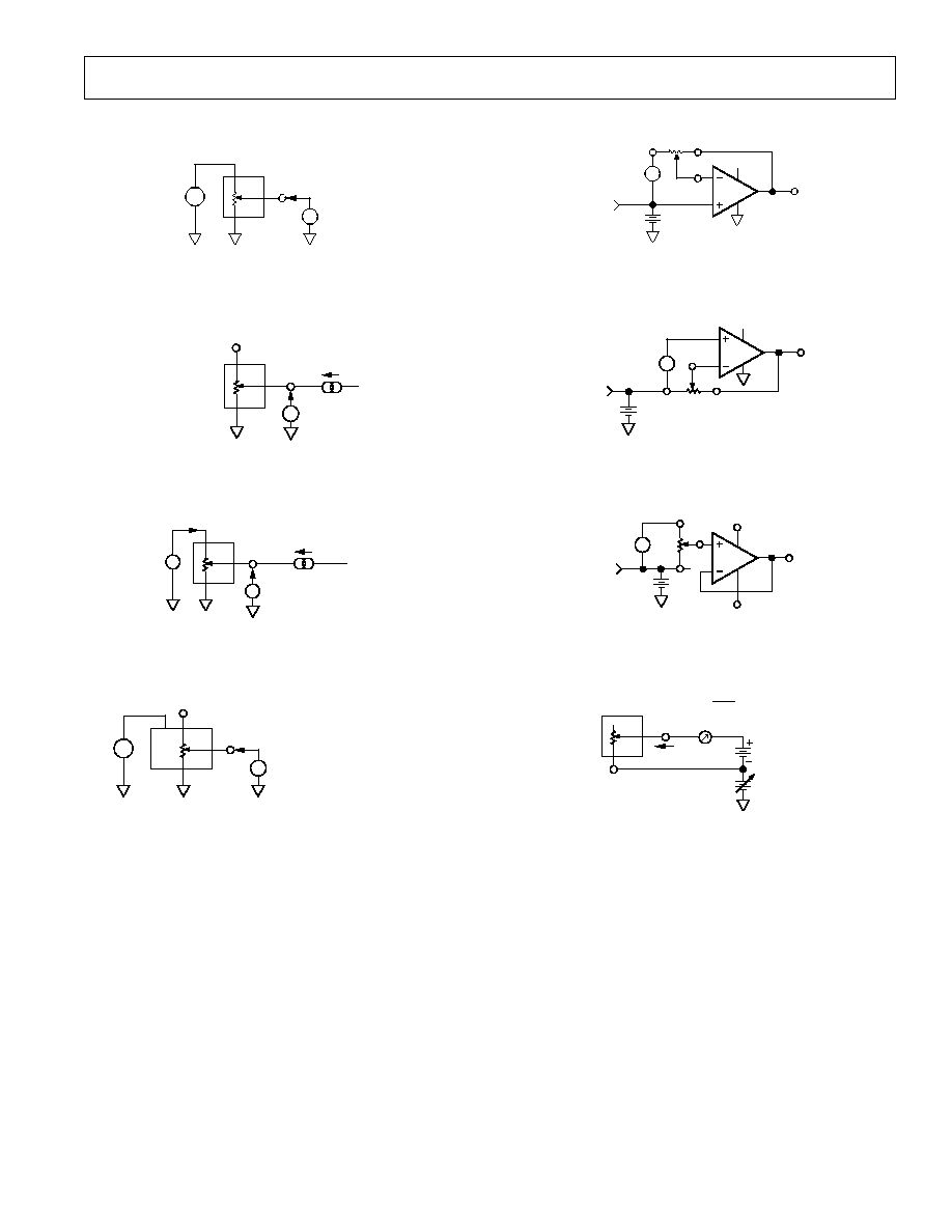
V+
DUT
V
MS
A
B
W
V+ = V
DD
1LSB = V+/128
Figure 27. Potentiometer Divider Nonlinearity Error Test
Circuit (INL, DNL)
NO CONNECT
I
W
DUT
V
MS
A
B
W
Figure 28. Resistor Position Nonlinearity Error (Rheostat
Operation; R-INL, R-DNL)
V
MS2
V
W
I
W
=
V
DD
/R
NOMINAL
DUT
V
MS1
A
B
W
R
W
= [V
MS1
V
MS2
]/I
W
Figure 29. Wiper Resistance Test Circuit
PSRR (dB) = 20 LOG
(
)
PSS (%/%) =
V
MS
V
DD
V
MS
%
V
DD
%
V+ = V
DD
± 10%
V
DD
V
A
~
V+
V
MS
A
B
W
Figure 30. Power Supply Sensitivity Test Circuit (PSS,
PSRR)
~
A
B
V
IN
2.5V DC
OP279
+5V
V
OUT
DUT
W
OFFSET
GND
Figure 31. Inverting Programmable Gain Test Circuit
~
A
B
V
IN
2.5V
OP279
+5V
V
OUT
DUT
W
OFFSET
GND
Figure 32. Noninverting Programmable Gain Test Circuit
A
B
2.5V
DUT
W
OFFSET
GND
~
V
IN
OP42
+15V
V
OUT
15V
Figure 33. Gain vs. Frequency Test Circuit
I
SW
0 TO V
DD
R
SW
=
0.1V
I
SW
CODE = ØØ
H
0.1V
DUT
B
W
Figure 34. Incremental ON Resistance Test Circuit
Parametric Test Circuits
AD5220
8
REV. 0
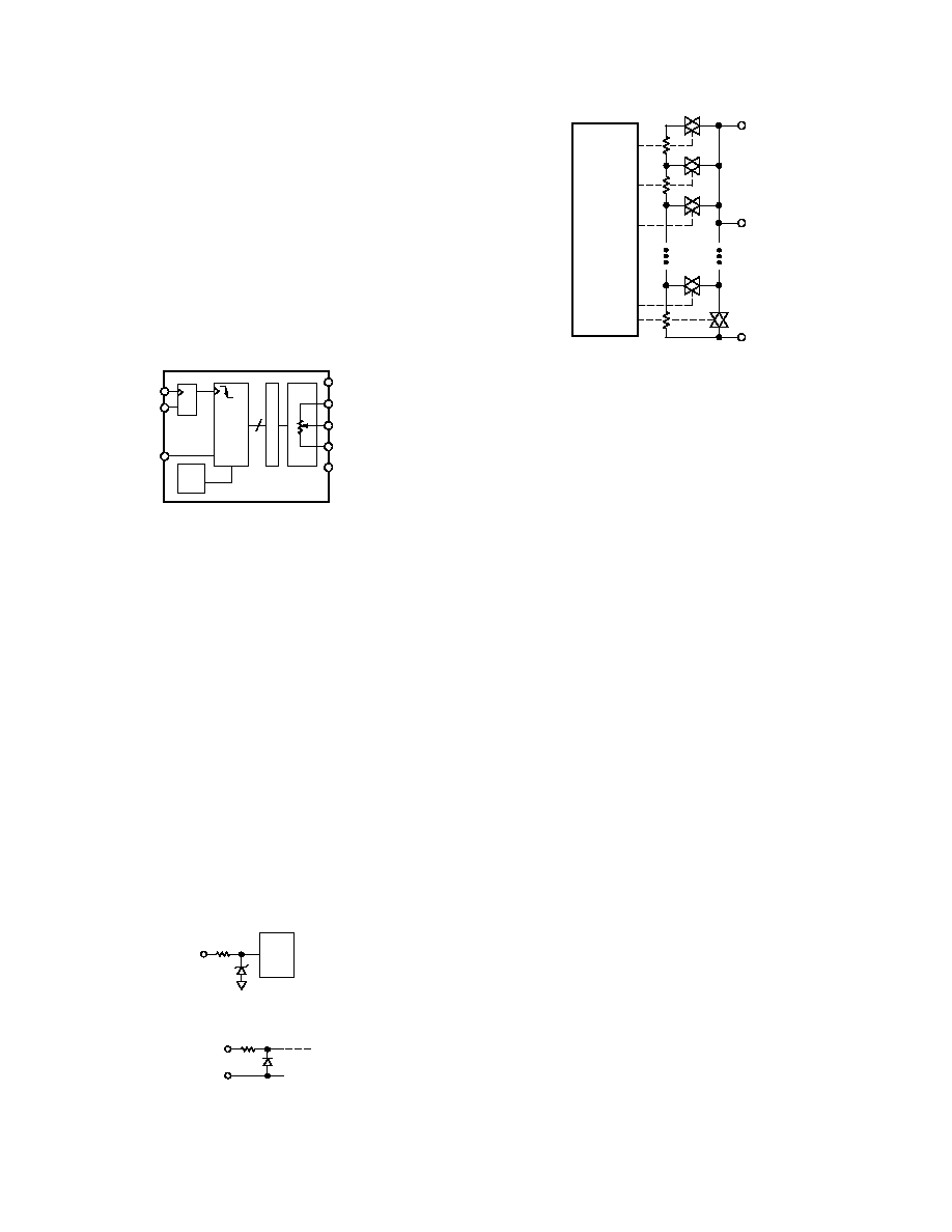
OPERATION
The AD5220 provides a 128-position digitally controlled vari-
able resistor (VR) device. Changing the VR settings is accom-
plished by pulsing the CLK pin while CS is active low. The
direction of the increment is controlled by the U/D (UP/DOWN)
control input pin. When the wiper hits the end of the resistor
(Terminals A or B) additional CLK pulses no longer change
the wiper setting. The wiper position is immediately decoded
by the wiper decode logic changing the wiper resistance. Ap-
propriate debounce circuitry is required when push button
switches are used to control the count sequence and direction
of count. The exact timing requirements are shown in Figure 3.
The AD5220 powers ON in a centered wiper position exhibit-
ing nearly equal resistances of R
WA
and R
WB
.
UP/
DOWN
CNTR
RS
D
E
C
O
D
E
7
40
H
POR
EN
AD5220
V
DD
A
W
B
GND
CLK
CS
U/
D
Figure 35. Block Diagram
DIGITAL INTERFACING OPERATION
The AD5220 contains a three-wire serial input interface. The
three inputs are clock (CLK), CS and UP/DOWN (U/D). The
negative-edge sensitive CLK input requires clean transitions to
avoid clocking multiple pulses into the internal UP/DOWN
counter register, see Figure 35. Standard logic families work
well. If mechanical switches are used for product evaluation
they should be debounced by a flip-flop or other suitable
means. When CS is taken active low the clock begins to incre-
ment or decrement the internal UP/DOWN counter dependent
upon the state of the U/D control pin. The UP/DOWN counter
value (D) starts at 40
H
at system power ON. Each new CLK
pulse will increment the value of the internal counter by one
LSB until the full scale value of 3F
H
is reached as long as the
U/D pin is logic high. If the U/D pin is taken to logic low the
counter will count down stopping at code 00
H
(zero-scale).
Additional clock pulses on the CLK pin are ignored when the
wiper is at either the 00
H
position or the 3F
H
position.
All digital inputs (CS, U/D, CLK) are protected with a series
input resistor and parallel Zener ESD structure shown in
Figure 36.
LOGIC
1k
Figure 36. Equivalent ESD Protection Digital Pins
20
A, B, W
GND
Figure 37. Equivalent ESD Protection Analog Pins
D0
D1
D2
D3
D4
D5
D6
RDAC
UP/DOWN
CNTR
&
DECODE
Wx
Bx
R
S
= R
NOMINAL
/128
R
S
R
S
R
S
Ax
Figure 38. AD5220 Equivalent RDAC Circuit
PROGRAMMING THE VARIABLE RESISTOR
Rheostat Operation
The nominal resistance of the RDAC between terminals A and
B is available with values of 10 k
, 50 k
, and 100 k
. The
final three characters of the part number determine the nominal
resistance value, e.g., 10 k
=10; 50 k
= 50; 100 k
= 100.
The nominal resistance (R
AB
) of the VR has 128 contact points
accessed by the wiper terminal, plus the B terminal contact. At
power ON the resistance from the wiper to either end Terminal
A or B is approximately equal. Clocking the CLK pin will in-
crease the resistance from the Wiper W to Terminal B by one
unit of R
S
resistance (see Figure 38). The resistance R
WB
is
determined by the number of pulses applied to the clock pin.
Each segment of the internal resistor string has a nominal resis-
tance value of R
S
= R
AB
/128, which becomes 78
in the case of
the 10 k
AD5220BN10 product. Care should be taken to limit
the current flow between W and B in the direct contact state to
a maximum value of 5 mA to avoid degradation or possible de-
struction of the internal switch contact.
Like the mechanical potentiometer the RDAC replaces, it is
totally symmetrical (see Figure 38). The resistance between the
Wiper W and Terminal A also produces a digitally controlled
resistance R
WA
. When these terminals are used the Bterminal
should be tied to the wiper.
The typical part-to-part distribution of R
BA
is process lot depen-
dent having a
±
30% variation. The change in R
BA
with tempera-
ture has a 800 ppm/
°
C temperature coefficient.
The R
BA
temperature coefficient increases as the wiper is pro-
grammed near the B-terminal due to the larger percentage con-
tribution of the wiper contact switch resistance, which has a
0.5%/
°
C temperature coefficient. Figure 14 shows the effect of
the wiper contact resistance as a function of code setting. An-
other performance factor influenced by the switch contact resis-
tance is the relative linearity error performance between the
10 k
, and the 50 k
or 100 k
versions. The same switch
contact resistance is used in all three versions. Thus the perfor-
mance of the 50 k
and 100 k
devices which have the least
impact on wiper switch resistance exhibits the best linearity
error, see Figures 7 and 8.

AD5220
9
REV. 0
PROGRAMMING THE POTENTIOMETER DIVIDER
Voltage Output Operation
The digital potentiometer easily generates an output voltage
proportional to the input voltage applied to a given terminal.
For example connecting A Terminal to +5 V and B Terminal to
ground produces an output voltage at the wiper which can be
any value starting at zero volts up to 1 LSB less than +5 V. Each
LSB of voltage is equal to the voltage applied across terminals
AB divided by the 128-position resolution of the potentiometer
divider. The general equation defining the output voltage with
respect to ground for any given input voltage applied to termi-
nals AB is:
V
W
(D) = D/128
×
V
AB
+ V
B
(1)
D represents the current contents of the internal UP/DOWN
counter.
Operation of the digital potentiometer in the divider mode re-
sults in more accurate operation over temperature. Here the
output voltage is dependent on the ratio of the internal resistors,
not the absolute value, therefore, the drift improves to 20 ppm/
°
C.
APPLICATIONS INFORMATION
The negative-edge sensitive CLK pin does not contain any
internal debounce circuitry. This standard CMOS logic input
responds to fast negative edges and needs to be debounced
externally with an appropriate circuit designed for the type of
switch closure device being used. Good performance results at
the CLK input pin when the negative logic transition has a
minimum slew rate of 1 V/
µ
s. A wide variety of standard circuits
can be used such as a one-shot multivibrator, Schmitt Triggered
gates, cross coupled flip-flops, or RC filters to drive the CLK
pin with uniform negative edges. This will prevent the digital
potentiometer from skipping output codes while counting due to
switch contact bounce.
AD5220
10
REV. 0
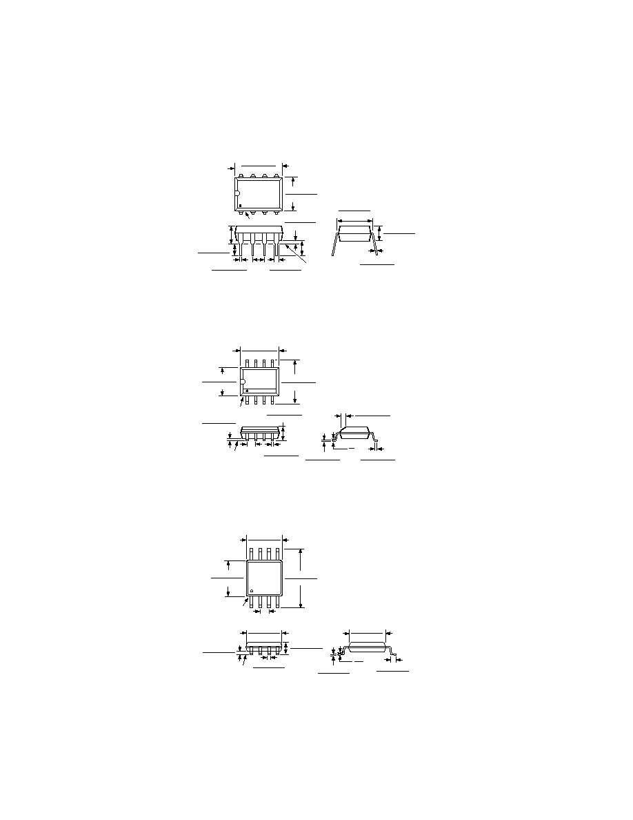
OUTLINE DIMENSIONS
Dimensions shown in inches and (mm).
8-Lead Plastic DIP
(N-8)
8
1
4
5
0.430 (10.92)
0.348 (8.84)
0.280 (7.11)
0.240 (6.10)
PIN 1
SEATING
PLANE
0.022 (0.558)
0.014 (0.356)
0.060 (1.52)
0.015 (0.38)
0.210 (5.33)
MAX
0.130
(3.30)
MIN
0.070 (1.77)
0.045 (1.15)
0.100
(2.54)
BSC
0.160 (4.06)
0.115 (2.93)
0.325 (8.25)
0.300 (7.62)
0.015 (0.381)
0.008 (0.204)
0.195 (4.95)
0.115 (2.93)
8-Lead SOIC
(SO-8)
0.1968 (5.00)
0.1890 (4.80)
8
5
4
1
0.2440 (6.20)
0.2284 (5.80)
PIN 1
0.1574 (4.00)
0.1497 (3.80)
0.0688 (1.75)
0.0532 (1.35)
SEATING
PLANE
0.0098 (0.25)
0.0040 (0.10)
0.0192 (0.49)
0.0138 (0.35)
0.0500
(1.27)
BSC
0.0098 (0.25)
0.0075 (0.19)
0.0500 (1.27)
0.0160 (0.41)
8
0
0.0196 (0.50)
0.0099 (0.25)
45
8-Lead SOIC
(RM-8)
8
5
4
1
0.122 (3.10)
0.114 (2.90)
0.199 (5.05)
0.187 (4.75)
PIN 1
0.0256 (0.65) BSC
0.122 (3.10)
0.114 (2.90)
SEATING
PLANE
0.006 (0.15)
0.002 (0.05)
0.018 (0.46)
0.008 (0.20)
0.043 (1.09)
0.037 (0.94)
0.120 (3.05)
0.112 (2.84)
0.011 (0.28)
0.003 (0.08)
0.028 (0.71)
0.016 (0.41)
33
27
0.120 (3.05)
0.112 (2.84)
C3426810/98
PRINTED IN U.S.A.