Document Outline
- FEATURES
- APPLICATIONS
- GENERAL DESCRIPTION
- SPECIFICATIONS
- ABSOLUTE MAXIMUM RATINGS
- ORDERING GUIDE
- PIN CONFIGURATION
- PIN FUNCTION DESCRIPTIONS
- TYPICAL PERFORMANCE CHARACTERISTICS
- OPERATIONAL OVERVIEW
- Scratch Pad and EEMEM Programming
- Basic Operation
- EEMEM Protection
- Digital Input/Output Configuration
- Serial Data Interface
- Daisy-Chain Operation
- Terminal Voltage Operation Range
- Power-Up Sequence
- Latched Digital Outputs
- ADVANCED CONTROL MODES
- Linear Increment and Decrement Commands
- Logarithmic Taper Mode Adjustment
- Using Additional Internal Nonvolatile EEMEM
- RDAC STRUCTURE
- PROGRAMMING THE VARIABLE RESISTOR
- PROGRAMMING THE POTENTIOMETER DIVIDER
- PROGRAMMING EXAMPLES
- TEST CIRCUITS
- FLASH/EEMEM RELIABILITY
- APPLICATIONS
- Bipolar Operation From Dual Supplies
- High Voltage Operation
- Bipolar Programmable Gain Amplifier
- 10-Bit Bipolar DAC
- Programmable Voltage Reference
- Programmable Voltage Source with Boosted Output
- Programmable 4 mA to 20 mA Current Source
- Programmable Bidirectional Current Source
- Resistance Scaling
- RDAC CIRCUIT SIMULATION MODEL
- DIGITAL POTENTIOMETER FAMILY SELECTION GUIDE
- OUTLINE DIMENSIONS
REV. 0
Information furnished by Analog Devices is believed to be accurate and
reliable. However, no responsibility is assumed by Analog Devices for its
use, nor for any infringements of patents or other rights of third parties that
may result from its use. No license is granted by implication or otherwise
under any patent or patent rights of Analog Devices.
a
AD5231
*
One Technology Way, P.O. Box 9106, Norwood, MA 02062-9106, U.S.A.
Tel: 781/329-4700
www.analog.com
Fax: 781/326-8703
© Analog Devices, Inc., 2001
Nonvolatile Memory,
1024-Position Digital Potentiometers
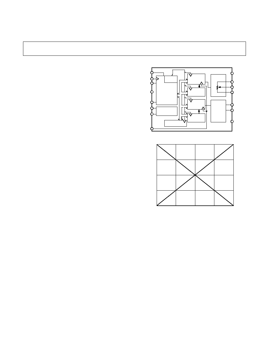
FUNCTIONAL BLOCK DIAGRAM
RDAC
REGISTER
EEMEM1
DIGITAL
REGISTER
EEMEM
CONTROL
28 BYTES
USER EEMEM
EEMEM2
AD5231
RDAC
DIGITAL
OUTPUT
BUFFER
CS
CLK
WP
PR
SDI
GND
SDO
RDY
SDO
SERIAL
INTERFACE
ADDR
DECODE
V
DD
V
SS
A
W
B
O1
O2
SDI
2
CODE ≠ Decimal
100
75
0
0
1023
256
R
WA
(D),
R
WB
(D) ≠ P
e
r
cent of Nominal ≠ % R
AB
512
768
50
25
R
WB
R
WA
Figure 1. R
WA
(D) and R
WB
(D) vs. Decimal Code
FEATURES
Nonvolatile Memory
1
Preset Maintains Wiper Settings
1024-Position Resolution
Full Monotonic Operation
10 k , 50 k , and 100 k Terminal Resistance
Permanent Memory Write-Protection
Wiper Settings Read Back
Linear Increment/Decrement
Log Taper Increment/Decrement
Push Button Increment/Decrement Compatible
SPI Compatible Serial Interface with Readback Function
3 V to 5 V Single Supply or 2.5 V Dual Supply
28 Bytes User Nonvolatile Memory for Constant Storage
100 Year Typical Data Retention T
A
= 55 C
APPLICATIONS
Mechanical Potentiometer Replacement
Instrumentation: Gain, Offset Adjustment
Programmable Voltage to Current Conversion
Programmable Filters, Delays, Time Constants
Line Impedance Matching
Power Supply Adjustment
Low Resolution DAC Replacement
GENERAL DESCRIPTION
The AD5231 provides nonvolatile memory digitally controlled
potentiometers
2
with 1024-position resolution. These devices
perform the same electronic adjustment function as a mechanical
potentiometer. The AD5231's versatile programming via a stan-
dard 3-wire serial interface allows 16 modes of operation and
adjustment, including scratch pad programming, memory stor-
ing and retrieving, increment/decrement, log taper adjustment,
wiper setting read back, and extra user-defined EEMEM.
In the scratch pad programming mode, a specific setting can be
programmed directly to the RDAC
2
register, which sets the resis-
tance at terminals W-A and W-B. The RDAC register can also
be loaded with a value previously stored in the EEMEM
1
regis-
ter. The value in the EEMEM can be changed or protected.
When changes are made to the RDAC register, the value of the
new setting can be saved into the EEMEM. Thereafter, such value
will be transferred automatically to the RDAC register during
system power ON. It is enabled by the internal preset strobe.
EEMEM can also be retrieved through direct programming and
external preset pin control.
Other operations include linear step increment and decrement
commands such that the setting in the RDAC register can be
moved UP or DOWN, one step at a time. For logarithmic changes
in wiper setting, a left/right bit shift command adjusts the level
in
±6 dB steps.
The AD5231 is available in thin TSSOP-16 package. All parts
are guaranteed to operate over the extended industrial tempera-
ture range of ≠40
∞C to +85∞C.
NOTES
1
The terms Nonvolatile Memory and EEMEM are used interchangeably.
2
The terms Digital Potentiometer and RDAC are used interchangeably.
*Patent pending

REV. 0
≠2≠
AD5231≠SPECIFICATIONS
ELECTRICAL CHARACTERISTICS 10 k , 50 k , 100 k VERSIONS
Parameter
Symbol
Conditions
Min
Typ
1
Max
Unit
DC CHARACTERISTICS
RHEOSTAT MODE
Resistor Differential Nonlinearity
2
R-DNL
R
WB,
V
A
= NC, Monotonic
≠1
±1/2
+1.8
LSB
Resistor Integral Nonlinearity
2
R-INL
R
WB,
V
A
= NC
≠0.2
+0.2
% FS
Nominal Resistor Tolerance
R
WB
D = 3FF
H
≠40
+20
%
Resistance Temperature Coefficient
R
AB
/ T
600
ppm/
∞C
Wiper Resistance
R
W
I
W
= 100
µA, V
DD
= 5.5 V,
15
100
Code = Half-Scale
I
W
= 100
µA, V
DD
= 3 V,
50
Code = Half-Scale
DC CHARACTERISTICS
POTENTIOMETER DIVIDER MODE
Resolution
N
10
Bits
Differential Nonlinearity
3
DNL
Monotonic, T
A
= 25
∞C
≠1
±1/2
+1
LSB
Monotonic, T
A
= ≠40
∞C or +85∞C
≠1
+1.25
LSB
Integral Nonlinearity
3
INL
≠0.4
+0.4
% FS
Voltage Divider Temperature Coefficient
V
W
/ T
Code = Half-Scale
15
ppm/
∞C
Full-Scale Error
V
WFSE
Code = Full-Scale
≠3
0
% FS
Zero-Scale Error
V
WZSE
Code = Zero-Scale
0
+1.5
% FS
RESISTOR TERMINALS
Terminal Voltage Range
4
V
A, B, W
V
SS
V
DD
V
Capacitance
5
A, B
C
A, B
f = 1 MHz, Measured to GND,
50
pF
Code = Half-Scale
Capacitance
5
W
C
W
f = 1 MHz, Measured to GND,
50
pF
Code = Half-Scale
Common-Mode Leakage Current
5, 6
I
CM
V
W
= V
DD
/2
0.01
1
µA
DIGITAL INPUTS and OUTPUTS
Input Logic High
V
IH
With Respect to GND, V
DD
= 5 V
2.4
V
Input Logic Low
V
IL
With Respect to GND, V
DD
= 5 V
0.8
V
Input Logic High
V
IH
With Respect to GND, V
DD
= 3 V
2.1
V
Input Logic Low
V
IL
With Respect to GND, V
DD
= 3 V
0.6
V
Input Logic High
V
IH
With Respect to GND,
V
DD
= +2.5 V, V
SS
= ≠2.5 V
2.0
V
Input Logic Low
V
IL
With Respect to GND,
V
DD
= +2.5 V, V
SS
= ≠2.5 V
0.5
V
Output Logic High (SDO, RDY)
V
OH
R
PULL-UP
= 2.2 k
to 5 V
4.9
V
Output Logic Low
V
OL
I
OL
= 1.6 mA, V
LOGIC
= 5 V
0.4
V
Input Current
I
IL
V
IN
= 0 V or V
DD
±2.5
µA
Input Capacitance
5
C
IL
4
pF
Output Current
5
I
O1,
I
O2
V
DD
= 5 V, V
SS
= 0 V, T
A
= 25
∞C
50
mA
V
DD
= 2.5 V, V
SS
= 0 V, T
A
= 25
∞C
7
mA
POWER SUPPLIES
Single-Supply Power Range
V
DD
V
SS
= 0 V
2.7
5.5
V
Dual-Supply Power Range
V
DD
/V
SS
±2.25
±2.75
V
Positive Supply Current
I
DD
V
IH
= V
DD
or V
IL
= GND
2.7
10
µA
Programming Mode Current
I
DD(PG)
V
IH
= V
DD
or V
IL
= GND
40
mA
Read Mode Current
7
I
DD(XFR)
V
IH
= V
DD
or V
IL
= GND
0.3
3
9
mA
Negative Supply Current
I
SS
V
IH
= V
DD
or V
IL
= GND,
V
DD
= +2.5 V, V
SS
= ≠2.5 V
0.5
10
µA
Power Dissipation
8
P
DISS
V
IH
= V
DD
or V
IL
= GND
0.018
0.05
mW
Power Supply Sensitivity
5
I
O
I
OL
P
SS
V
DD
= 5 V
± 10%
0.002
0.01
%/%
DYNAMIC CHARACTERISTICS
5, 9
Bandwidth
BW
≠3 dB, R = 10 k
/50 k/100 k
370/85/44
kHz
Total Harmonic Distortion
THD
W
V
A
= 1 V
RMS
, V
B
= 0 V, f = 1 kHz,
R
AB
= 10 k
0.022
%
Total Harmonic Distortion
THD
W
V
A
= 1 V
RMS
, V
B
= 0 V, f = 1 kHz,
R
AB
= 50 k
, 100 k
0.045
%
(V
DD
= 3 V
10% or 5 V 10% and V
SS
= 0 V, V
A
= +V
DD
, V
B
= 0 V, ≠40 C < T
A
< +85 C, unless otherwise noted.)

REV. 0
≠3≠
AD5231
Parameter
Symbol
Conditions
Min
Typ
1
Max
Unit
V
W
Settling Time
t
S
V
A
= V
DD
, V
B
= 0 V,
1.2/3.7/7
µs
V
W
= 0.50% Error Band,
Code 000
H
to 200
H
For R
AB
= 10 k
/50 k
/100 k
Resistor Noise Voltage
e
N_WB
R
WB
= 5 k
, f = 1 kHz
9
nV/
Hz
NOTES
1
Typicals represent average readings at 25 C and V
DD
= 5 V.
2
Resistor position nonlinearity error R-INL is the deviation from an ideal value measured between the maximum resistance and the minimum resistance wiper positions.
R-DNL measures the relative step change from ideal between successive tap positions. I
W
~ 50
µA @ V
DD
= +2.7 V and I
W
~ 400
µA @ V
DD
= +5 V for the R
AB
= 10 k
version, I
W
~ 50 A for the R
AB
= 50 k
and I
W
~ 25 A for the R
AB
= 100 k
version. See test circuit Figure 12.
3
INL and DNL are measured at V
W
with the RDAC configured as a potentiometer divider similar to a voltage output D/A converter. V
A
= V
DD
and V
B
= V
SS
. DNL
specification limits of ≠1 LSB minimum are Guaranteed Monotonic operating conditions. See test circuit Figure 13.
4
Resistor terminals A, B, and W have no limitations on polarity with respect to each other. Dual Supply Operat ion enables ground-referenced bipolar signal adjustment.
5
Guaranteed by design and not subject to production test.
6
Common-mode leakage current is a measure of the dc leakage from any terminal B and W to a common-mode bias level of V
DD
/2.
7
Transfer (XFR) Mode current is not continuous. Current consumed while EEMEM locations are read and transferred to the RDAC register. See TPC 19.
8
P
DISS
is calculated from (I
DD
V
DD
) + (I
SS
V
SS
).
9
All dynamic characteristics use V
DD
= +2.5 V and V
SS
= ≠2.5 V.
Specifications subject to change without notice.
ELECTRICAL CHARACTERISTICS 10 k , 50 k , 100 k VERSIONS
Parameter
Symbol
Conditions
Min
Typ
1
Max
Unit
INTERFACE TIMING
CHARACTERISTICS
2, 3
Clock Cycle Time (t
CYC
)
t
1
20
ns
CS Setup Time
t
2
10
ns
CLK Shutdown Time to
CS Rise
t
3
1
t
CYC
Input Clock Pulsewidth
t
4
, t
5
Clock Level High or Low
10
ns
Data Setup Time
t
6
From Positive CLK Transition
5
ns
Data Hold Time
t
7
From Positive CLK Transition
5
ns
CS to SDO-SPI Line Acquire
t
8
40
ns
CS to SDO-SPI Line Release
t
9
50
ns
CLK to SDO Propagation Delay
4
t
10
R
P
= 2.2 k
, C
L
< 20 pF
50
ns
CLK to SDO Data Hold Time
t
11
R
P
= 2.2 k
, C
L
< 20 pF
0
ns
CS High Pulsewidth
5
t
12
10
ns
CS High to CS High
5
t
13
4
t
CYC
RDY Rise to
CS Fall
t
14
0
ns
CS Rise to RDY Fall Time
t
15
0.1
0.15
ms
Read/Store to Nonvolatile EEMEM
6
t
16
Applies to Command 2
H
, 3
H
, 9
H
25
ms
CS Rise to Clock Rise/Fall Setup
t
17
10
ms
Preset Pulsewidth (Asynchronous)
t
PRW
Not Shown in Timing Diagram
50
ms
Preset Response Time to RDY High
t
PRESP
PR Pulsed Low to Refreshed
Wiper Positions
70
µs
FLASH/EE MEMORY RELIABILITY
Endurance
7
100
K Cycles
Data Retention
8
100
Years
NOTES
1
Typicals represent average readings at 25 C and V
DD
= 5 V.
2
Guaranteed by design and not subject to production test.
3
See timing diagram for location of measured values. All input control voltages are specified with t
R
= t
F
= 2.5 ns (10% to 90% of 3 V) and timed from a voltage level
of 1.5 V. Switching characteristics are measured using both V
DD
= 3 V and 5 V.
4
Propagation delay depends on value of V
DD
, R
PULL_UP
, and C
L
. See applications text.
5
Valid for commands that do not activate the RDY pin.
6
RDY pin low only for commands 2, 3, 8, 9, 10, and the PR hardware pulse: CMD_8 ~ 1 s; CMD_9,10 ~0.12 s; CMD_2,3 ~20 s. Device operation at T
A
= ≠40 C
and V
DD
< +3 V extends the save time to 35 s.
7
Endurance is qualified to 100,000 cycles as per JEDEC Std. 22 method A117 and measured at ≠40 C, +25 C, and +85 C; typical endurance at 25 C is 700,000 cycles.
8
Retention lifetime equivalent at junction temperature (T
J
) = 55 C as per JEDEC Std. 22, Method A117. Retention lifetime based on an activation energy of 0.6 eV
will derate with junction temperature as shown in Figure 20 in the Flash/EE Memory Description section of this data sheet. The AD5231 contains 9,646 transistors.
Die size: 69 mil 115 mil, 7,993 sq. mil.
Specifications subject to change without notice.
(V
DD
= 3 V to 5.5 V and ≠40 C < T
A
< +85 C, unless otherwise noted.)
REV. 0
AD5231
≠4≠
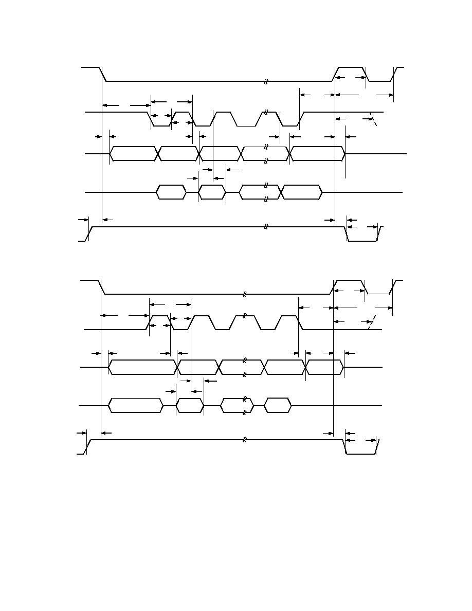
CPOL = 1
t
12
t
13
t
3
t
17
t
9
t
11
t
5
t
4
t
2
t
1
CLK
t
8
*
MSB
LSB OUT
MSB
LSB
RDY
CPHA = 1
t
10
t
7
t
6
t
14
t
15
t
16
*NOT DEFINED, BUT NORMALLY LSB OF CHARACTER PREVIOUSLY TRANSMITTED.
THE CPOL = 1 MICROCONTROLLER COMMAND ALIGNS THE INCOMING DATA TO THE POSITIVE EDGE OF THE CLOCK.
CS
SDO
SDI
Figure 2a. CPHA = 1 Timing Diagram
t
12
t
13
t
3
t
17
t
9
t
11
t
5
t
4
t
2
t
1
CLK
CPOL = 0
t
8
MSB OUT
LSB
SDO
MSB IN
LSB
SDI
RDY
CPHA = 0
t
10
t
7
t
6
t
14
t
15
t
16
*NOT DEFINED, BUT NORMALLY MSB OF CHARACTER JUST RECEIVED.
THE CPOL = 0 MICROCONTROLLER COMMAND ALIGNS THE INCOMING DATA TO THE POSITIVE EDGE OF THE CLOCK.
*
CS
Figure 2b. CPHA = 0 Timing Diagram

REV. 0
AD5231
≠5≠
ABSOLUTE MAXIMUM RATIN
GS
1
(T
A
= 25
∞C, unless otherwise noted)
V
DD
to GND . . . . . . . . . . . . . . . . . . . . . . . . . . . ≠0.3 V, +7 V
V
SS
to GND . . . . . . . . . . . . . . . . . . . . . . . . . . . . +0.3 V, ≠7 V
V
DD
to V
SS
. . . . . . . . . . . . . . . . . . . . . . . . . . . . . . . . . . . . . 7 V
V
A
, V
B
, V
W
to GND . . . . . . . . . . . . . V
SS
≠ 0.3 V, V
DD
+ 0.3 V
A≠B, A≠W, B≠W
Intermittent
2
. . . . . . . . . . . . . . . . . . . . . . . . . . . . .
±20 mA
Continuous . . . . . . . . . . . . . . . . . . . . . . . . . . . . . . .
±2 mA
Digital Inputs and Output Voltage to GND
. . . . . . . . . . . . . . . . . . . . . . . . . . . . . . ≠0.3 V, V
DD
+ 0.3 V
Operating Temperature Range
3
. . . . . . . . . . . ≠40
∞C to +85∞C
Maximum Junction Temperature (T
J
Max) . . . . . . . . . 150
∞C
Storage Temperature . . . . . . . . . . . . . . . . . . ≠65
∞C to +150∞C
Lead Temperature, Soldering
Vapor Phase (60 sec) . . . . . . . . . . . . . . . . . . . . . . . 215
∞C
Infrared (15 sec) . . . . . . . . . . . . . . . . . . . . . . . . . . . 220
∞C
Thermal Resistance Junction-to-Ambient
JA
,
TSSOP-16 . . . . . . . . . . . . . . . . . . . . . . . . . . . . . 150
∞C/W
Thermal Resistance Junction-to-Case
JC
,
TSSOP-16 . . . . . . . . . . . . . . . . . . . . . . . . . . . . . . 28
∞C/W
Package Power Dissipation = (T
J
Max ≠ T
A
)/
JA
NOTES
1
Stresses above those listed under Absolute Maximum Ratings may cause perma-
nent damage to the device. This is a stress rating; functional operation of the device
at these or any other conditions above those listed in the operational sections of this
specification is not implied. Exposure to absolute maximum rating conditions for
extended periods may affect device reliability.
2
Maximum terminal current is bounded by the maximum current handling of the
switches, maximum power dissipation of the package, and maximum applied
voltage across any two of the A, B, and W terminals at a given resistance.
3
Includes programming of nonvolatile memory
WARNING!
ESD SENSITIVE DEVICE
CAUTION
ESD (electrostatic discharge) sensitive device. Electrostatic charges as high as 4000 V readily
accumulate on the human body and test equipment and can discharge without detection. Although
the AD5231 features proprietary ESD protection circuitry, permanent damage may occur on
devices subjected to high-energy electrostatic discharges. Therefore, proper ESD precautions are
recommended to avoid performance degradation or loss of functionality.
ORDERING GUIDE
R
AB
Temperature
Package
Package
Ordering
Model
(k ) Range ( C)
Description
Option
Quantity
Top Mark
*
AD5231BRU10
10
≠40 to +85
TSSOP-16
RU-16
96
5231B10
AD5231BRU10-REEL7
10
≠40 to +85
TSSOP-16
RU-16
1,000
5231B10
AD5231BRU50
50
≠40 to +85
TSSOP-16
RU-16
96
5231B50
AD5231BRU50-REEL7
50
≠40 to +85
TSSOP-16
RU-16
1,000
5231B50
AD5231BRU100
100
≠40 to +85
TSSOP-16
RU-16
96
5231BC
AD5231BRU100-REEL7
100
≠40 to +85
TSSOP-16
RU-16
1,000
5231BC
*Line 1 contains ADI logo symbol and the date code YYWW; line 2 contains detail model number listed in this column.