PRELIMINARY TECHNICAL DATA
a
Nonvolatile Memory, Dual 1024
Position Digital Potentiometers
AD5235
REV PrD 6 Nov 2000
Information furnished by Analog Devices is believed to be accurate and reliable. However, no
responsibility is assumed by Analog Devices for its use; nor for any infringements of patents or
other rights of third parties which may result from its use. No license is granted by implication
or otherwise under any patent or patent rights of Analog Devices.
One Technology Way, P.O. Box 9106,
Norwood, MA 02062-9106 U
.
S
.
A
.
Tel: 781/329-4700
Fax:781/326-8703
FEATURES
Dual, 1024 Position Resolution
25K, 250K Ohm Terminal Resistance with 50ppm/�C Tempco
Nonvolatile Memory Preset
SPI Compatible Serial Data Input with Readback Function
Increment/Decrement Commands, Push Button Command
+3 to +5V Single Supply Operation
�2.5V Dual Supply Operation
30 bytes of general purpose nonvolatile memory
APPLICATIONS
Mechanical Potentiometer Replacement
Instrumentation: Gain, Offset Adjustment
Programmable Voltage to Current Conversion
Programmable Filters, Delays, Time Constants
Line Impedance Matching
Power Supply Adjustment
DIP Switch Setting
GENERAL DESCRIPTION
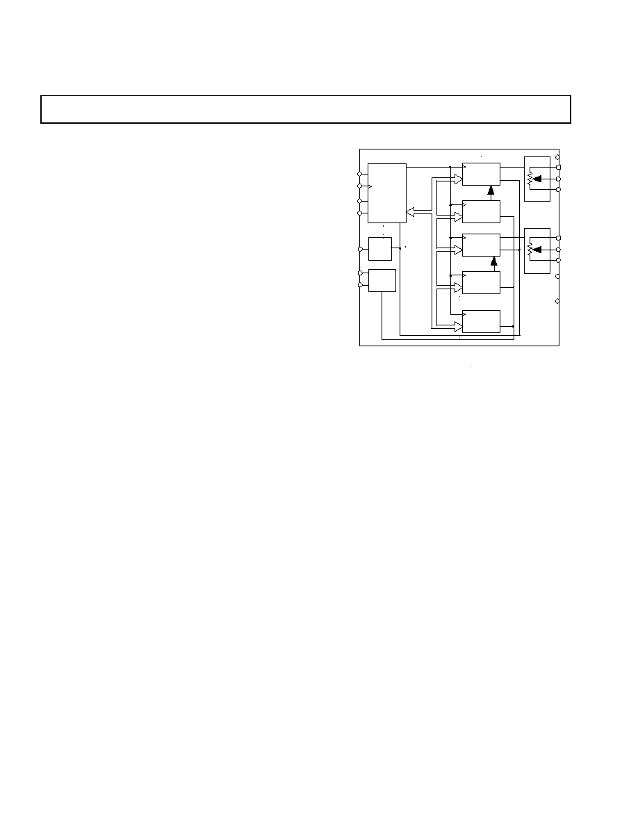
The AD5235 provides a dual channel, digitally controlled variable
resistor (VR) with resolutions of 1024 positions. These devices
perform the same electronic adjustment function as a potentiometer or
variable resistor. The AD5235's versatile programming via a Micro
Controller allows multiple modes of operation and adjustment.
In the direct program mode a predetermined setting of the RDAC
register can be loaded directly from the micro controller. Another key
mode of operation allows the RDAC register to be refreshed with the
setting previously stored in the EEMEM register. When changes are
made to the RDAC register to establish a new wiper position, the
value of the setting can be saved into the EEMEM by executing an
EEMEM save operation. Once the settings are saved in the EEMEM
register, these values will be transferred automatically to the RDAC
register to set the wiper position at system power ON. Such operation
is enabled by the internal preset strobe and the preset can also be
accessed externally.
An internal scratch pad RDAC register can be programmed by the
micro controller to set the resistance between terminals W-and-B.
Once the target value is achieved, the RDAC content register can be
placed in the non-volatile memory for automatic recall during Power
Up.
The AD5235 is available in the thin TSSOP-16 package. All parts are
guaranteed to operate over the extended industrial temperature range
of -40�C to +85�C.
FUNCTIONAL BLOCK DIAGRAMS
G ND
RDAC2
RDAC1
PWR ON
PRESET
S E R I A L
IN P U T
R E G IS T E R
RDAC1
REGISTER
PR
WP
CS
G ND
VDD
W1
A1
B1
VSS
ADDRESS
DECO DE
RDY
CLK
EEMEM1
W2
A2
B2
EEMEM2
EEMEM
CONTROL
RDAC2
REGISTER
SDI
SDO
SPARE
EEMEM

PRELIMINARY TECHNICAL DATA
Nonvolatile Memory Digital Potentiometers
AD5235
REV PrD 6 NOV, 2000
2
Information contained in this Product Concept data sheet describes a product in the early definition stage. There is no guarantee that the
information contained here will become a final product in its present form. For latest information contact Walt Heinzer/Analog Devices, Santa Clara,
CA. TEL(408)562-7254; FAX (408)727-1550; walt.heinzer@analog.com
ELECTRICAL CHARACTERISTICS 25K, 250K OHM VERSIONS
(V
DD
= +3V�10% or +5V�10% and V
SS
=0V, V
A
= +V
DD
, V
B
= 0V, -40�C < T
A
< +85�C unless otherwise noted.)
Parameter Symbol
Conditions
Min
Typ
1
Max
Units
DC CHARACTERISTICS RHEOSTAT MODE Specifications apply to all VRs
Resistor Differential NL
2
R-DNL
R
WB
, V
A
=NC -1
�1/4
+1
LSB
Resistor Nonlinearity
2
R-INL
R
WB
, V
A
=NC -2
�1/2
+2
LSB
Nominal resistor tolerance
R T
A
= 25�C, V
AB
= V
DD
,Wiper (V
W
) = No connect
-30
30
%
Resistance Temperature Coefficent
R
AB
/
T VAB = VDD, Wiper (V
W
) = No Connect
50
ppm/�C
Wiper Resistance
R
W
I
W
= 1 V/R, V
DD
= +5V
50
100
Wiper Resistance
R
W
I
W
= 1 V/R, V
DD
= +3V
200
DC CHARACTERISTICS POTENTIOMETER DIVIDER MODE Specifications apply to all VRs
Resolution N
10
Bits
Integral Nonlinearity
3
INL
�2
�1/2
+2
LSB
Differential Nonlinearity
3
DNL
�1
�1/4
+1
LSB
Voltage Divider Temperature Coefficent
V
W
/
T
Code = Half-scale
15
ppm/�C
Full-Scale Error
V
WFSE
Code = Full-scale
�3
-1
+0
LSB
Zero-Scale Error
V
WZSE
Code = Zero-scale
0
+1
+3
LSB
RESISTOR TERMINALS
Voltage Range
4
V
A,B,W
V
SS
V
DD
V
Capacitance
5
Ax, Bx
C
A,B
f = 1 MHz, measured to GND, Code = Half-scale
45
pF
Capacitance
5
Wx
C
W
f = 1 MHz, measured to GND, Code = Half-scale
60
pF
Common-mode Leakage Current
7
I
CM
V
A
= V
B
= V
DD
/2
0.01
1
�A
DIGITAL INPUTS & OUTPUTS
Input Logic High
V
IH
with respect to GND
0.3
�
V
DD
V
Input Logic Low
V
IL
with respect to GND
0.7
�
V
DD
V
Output Logic High
V
OH
R
PULL-UP
= 2.2K
to +5V
4.9
V
Output Logic High
V
OH
I
OH
= 40
�
A, V
LOGIC
= +5V
4
V
Output Logic Low
V
OL
I
OL
= 1.6mA, V
LOGIC
= +5V
0.4
V
Input Current
I
IL
V
IN
= 0V or V
DD
�1
�A
Input Capacitance
5
C
IL
5
pF
POWER SUPPLIES
Single-Supply Power Range
V
DD
V
SS
= 0V
2.7
5.5
V
Dual-Supply Power Range
V
DD
/V
SS
V
SS
= 0V
�2.2
�2.7
V
Positive Supply Current
I
DD
V
IH
= V
DD
or V
IL
= GND
2
20
�A
Programming Mode Current
I
DD(PG)
V
IH
= V
DD
or V
IL
= GND
15
mA
Read Mode Current
I
DD(READ)
V
IH
= V
DD
or V
IL
= GND
650
�A
Negative Supply Current
I
SS
V
IH
= V
DD
or V
IL
= GND, V
DD
= 2.5V, V
SS
= -2.5V
10
�A
Power Dissipation
6
P
DISS
V
IH
= V
DD
or V
IL
= GND
0.05
mW
Power Supply Sensitivity
PSS
V
DD
= +5V �10%
0.002
0.01
%/%
DYNAMIC CHARACTERISTICS
5, 7
Bandwidth �3dB
BW_25K
R = 12K
400
KHz
Total Harmonic Distortion
THD
W
V
A
=1Vrms, V
B
= 0V, f=1KHz
0.003
%
V
W
Settling Time
t
S
V
A
= VDD, V
B
=0V, 50% of final value
25K/250K
0.6/3/6
�s
Resistor Noise Voltage
e
N_WB
R
WB
= 10K
, f = 1KHz
9
nV
Hz
Crosstalk C
T
V
A
= V
DD
, V
B
= 0V, Measue V
W
with adjacent
VR making full scale change
-65
dB

PRELIMINARY TECHNICAL DATA
Nonvolatile Memory Digital Potentiometers
AD5235
REV PrD 6 NOV, 2000
3
Information contained in this Product Concept data sheet describes a product in the early definition stage. There is no guarantee that the
information contained here will become a final product in its present form. For latest information contact Walt Heinzer/Analog Devices, Santa Clara,
CA. TEL(408)562-7254; FAX (408)727-1550; walt.heinzer@analog.com
ELECTRICAL CHARACTERISTICS 25K, 250K OHM VERSIONS
(V
DD
= +3V�10% to +5V�10% and V
SS
=0V, V
A
= +V
DD
, V
B
= 0V, -40�C < T
A
< +85�C unless otherwise noted.)
Parameter Symbol
Conditions
Min
Typ
1
Max
Units
INTERFACE TIMING CHARACTERISTICS applies to all parts(Notes 5, 8)
Clock Cycle Time
t
1
20
ns
Input Clock Pulse Width
t
2
, t
3
Clock level high or low
10
ns
CS Setup Time
t
4
10
ns
Data Setup Time
t
5
From Positive CLK transition
5
ns
Data Hold Time
t
6
From Positive CLK transition
5
ns
CLK Shutdown Time
t
7
0
ns
CS Rise to Clock Rise Setup
t
8
10
ns
CS High Pulse Width
t
9
10
ns
CLK to SDO Propagation Delay
9
t
10
R
L
= 1K
, C
L
< 20pF
1
25
ns
Store to Nonvolatile EEMEM Save Time
10
t
11
Applies to Command 2
H
, 3
H
25
ms
CS to SDO - SPI line acquire
t
12
ns
CS to SDO - SPI line release
t
13
ns
RDY Rise to CLK Rise
t
14
ns
Startup Time
t
15
ms
CLK Setup Time
t
16
For 1 CLK period (t
4
- t
3
= 1 CLK period)
ns
Preset Pulse Width
t
PR
50
ns
NOTES:
1.
Typicals represent average readings at +25�C and V
DD
= +5V.
2.
Resistor position nonlinearity error R-INL is the deviation from an ideal value measured between the maximum resistance and the minimum resistance wiper positions. R-DNL measures the relative step
change from ideal between successive tap positions. Parts are guaranteed monotonic. See figure 20 test circuit. I
W
= V
DD
/R for both V
DD
=+3V or V
DD
=+5V.
3.
INL and DNL are measured at V
W
with the RDAC configured as a potentiometer divider similar to a voltage output D/A converter. V
A
= V
DD
and V
B
= 0V.
DNL specification limits of �1LSB maximum are Guaranteed Monotonic operating conditions. See Figure 19 test circuit.
4.
Resistor terminals A,B,W have no limitations on polarity with respect to each other.
5.
Guaranteed by design and not subject to production test.
6. P
DISS
is calculated from (I
DD
x V
DD
=+5V).
7.
All dynamic characteristics use V
DD
= +5V.
8.
See timing diagram for location of measured values. All input control voltages are specified with t
R
=t
F
=2.5ns(10% to 90% of 3V) and timed from a voltage level of 1.5V. Switching characteristics are
measured using both V
DD
= +3V or +5V.
9.
Propagation delay depends on value of V
DD
, R
PULL_UP
, and C
L
see applications text.
10.
Low only for commands 8, 9,10, 2, 3: CMD_8 ~ 1ms; CMD_9,10 ~0.1ms; CMD_2,3 ~20ms.
Timing Diagram
t
2
t
3
M S B
L S B
M S B
L S B
C L K
C S
S D I
S D O
1
t
1
t
4
t
5
t
6
t
7
t
9
t
13
t
10
R D Y
t
11
t
16
M S B
L S B
S D O
2
t
12
t
14
t
15
S DO
1
CLK IDLES LOW
S DO
2
CLK IDLES HIGH
t
8
Figure 1. Timing Diagram
PRELIMINARY TECHNICAL DATA
Nonvolatile Memory Digital Potentiometers
AD5235
REV PrD 6 NOV, 2000
4
Information contained in this Product Concept data sheet describes a product in the early definition stage. There is no guarantee that the
information contained here will become a final product in its present form. For latest information contact Walt Heinzer/Analog Devices, Santa Clara,
CA. TEL(408)562-7254; FAX (408)727-1550; walt.heinzer@analog.com
Absolute Maximum Rating (
T
A
= +25�C, unless otherwise
noted)
V
DD
to GND..............................................................-0.3, +7V
V
SS
to GND ................................................................. 0V, -7V
V
DD
to V
SS
......................................................................... +7V
V
A
, V
B
, V
W
to GND ................................................. V
SS
, V
DD
A
X
� B
X
, A
X
� W
X
, B
X
� W
X
...................................... �20mA
O
x
to GND ...................................................................0V, V
DD
Digital Inputs & Output Voltage to GND .................. 0V, +7V
Operating Temperature Range......................... -40�C to +85�C
Maximum Junction Temperature (T
J MAX
)...................+150�C
Storage Temperature ..................................... -65�C to +150�C
Lead Temperature (Soldering, 10 sec)..........................+300�C
Thermal Resistance
JA,
TSSOP-16...................................................... 180�C/W
Package Power Dissipation = (TJMAX - TA) /
JA
Ordering Guide
#CHs/
Temp
Package
Package
Model k
Ohm
Range
Description
Option
AD5235BRU25 X2/25 -40/+85�C
TSSOP-16 RU-16
AD5235BRU250 X2/250 -40/+85�C TSSOP-16
RU-16
The AD5235 contains 16,000 transistors.
Die size: 100 x 105 mil = 10,500 sq. mil
AD5235
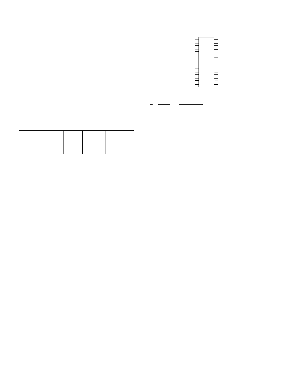
PIN CONFIGURATION
CLK
SDI
SDO
GND
V
SS
A1
W1
B1
RDY
CS
CS
CS
CS
PR
PR
PR
PR
WP
WP
WP
WP
V
DD
A2
W2
B2
16
15
14
13
12
11
10
9
1
2
3
4
5
6
7
8
AD5235 PIN FUNCTION DESCRIPTION
# Name Description
1
CLK
Serial Input Register clock pin. Shifts in one bit at
a time on positive clock edges.
2
SDI
Serial Data Input Pin. Shifts in one bit at a time
on positive clock CLK edges.
3
SDO
Serial Data Output Pin. Open Drain Output
requires external pull-up resistor. Commands 9
and 10 activate the SDO output. See Instruction
operation Truth Table. Table 2.
4
GND
Ground pin, logic ground reference
5 V
SS
Negative Supply. Connect to zero volts for single
supply applications.
6
A1
A terminal of RDAC1.
7
W1
Wiper terminal of RDAC1,
ADDR(RDAC1) = 0
H
.
8
B1
B terminal of RDAC1.
9
B2
B terminal of RDAC2.
10
W2
Wiper terminal of RDAC2,
ADDR(RDAC3) = 1
H
.
11
A2
A terminal of RDAC2.
12 V
DD
Positive Power Supply Pin. Should be
the
input-logic HIGH voltage.
13
WP
Write Protect Pin. Prevents any changes to the
present EEMEM contents when active low.
14
PR
Hardware over ride preset pin. Refreshes the
scratch pad register with current contents of the
EEMEM register. Factory default loads midscale
512
10
.
15
CS
Serial Register chip select active low. Serial
register operation takes place when
CS returns to
logic high.
16
RDY
Ready. Active-high open drain output. Identifies
completion of commands 2, 3, 8, 9, 10.
PRELIMINARY TECHNICAL DATA
Nonvolatile Memory Digital Potentiometers
AD5235
REV PrD 6 NOV, 2000
5
Information contained in this Product Concept data sheet describes a product in the early definition stage. There is no guarantee that the
information contained here will become a final product in its present form. For latest information contact Walt Heinzer/Analog Devices, Santa Clara,
CA. TEL(408)562-7254; FAX (408)727-1550; walt.heinzer@analog.com
OPERATIONAL OVERVIEW
The AD5235 digital potentiometer is designed to operate as a true
variable resistor replacement device for analog signals that remain
within the terminal voltage range of V
SS
<V
TERM
<V
DD
. The basic
voltage range is limited to a V
DD
- V
SS
<5.5V. Control of the digital
potentiometer allows both scratch pad register (RDAC register)
changes to be made, as well as 100,000 times of nonvolatile
electrically erasable memory (EEMEM) register operations. The
EEMEM update process takes approximately 20.2ms, during this
time the shift register is locked preventing any changes from taking
place. The RDY pin flags the completion of this EEMEM save.
The EEMEM retention is designed to last 10 years without refresh.
The scratch pad register can be changed incrementally by using the
software controlled Increment/Decrement instruction or the Shift
Left/Right instruction command. Once an Increment, Decrement or
Shift command has been loaded into the shift register, subsequent
CS strobes will repeat this command. This is useful for push button
control applications. Alternately the scratch pad register can be
programmed with any position value using the standard SPI serial
interface mode by loading the representative data word. The
scratch pad register can be loaded with the current contents of the
nonvolatile EEMEM register under the program control. At system
power ON, the default value of the scratch pad memory is the value
previously saved in the EEMEM register. The factory EEMEM
preset value is midscale 512
10
.
A serial data output pin is available for daisy chaining and for
readout of the internal register contents. The serial input data
register uses a 24-bit instruction/address/data WORD. The write-
protect (
WP) pin provides a hardware EEMEM protection feature
disabling any changes of the present EEMEM contents.
SERIAL DATA INTERFACE
The AD5235 contains a four-wire SPI compatible digital interface
(SDI, SDO,
CS, and CLK). Key features of this interface include:
�
Independently Programmable Read & Write to all registers
�
Direct parallel refresh of all RDAC wiper registers from
corresponding EEMEM registers
�
Permanent storage of the present scratch pad RDAC register
values into the corresponding EEMEM register
�
30 bytes of user addressable electrical-erasable memory
The serial interface of AD5235 digital potentiometer uses a 24-bit
serial word loaded with MSB first. The format of the SPI
compatible word is shown in Table 1. The Command Bits (Cx)
control the operation of the digital potentiometer according to the
command instruction shown in Table 2. The Address Bits (Ax)
determine which register is activated. The Data Bits (Dx) are the
values that are loaded into the decoded register. The last
instruction executed prior to a period of no programming activity
should be the NOP instruction. This will place the internal logic
circuitry in a minimum power dissipation state.
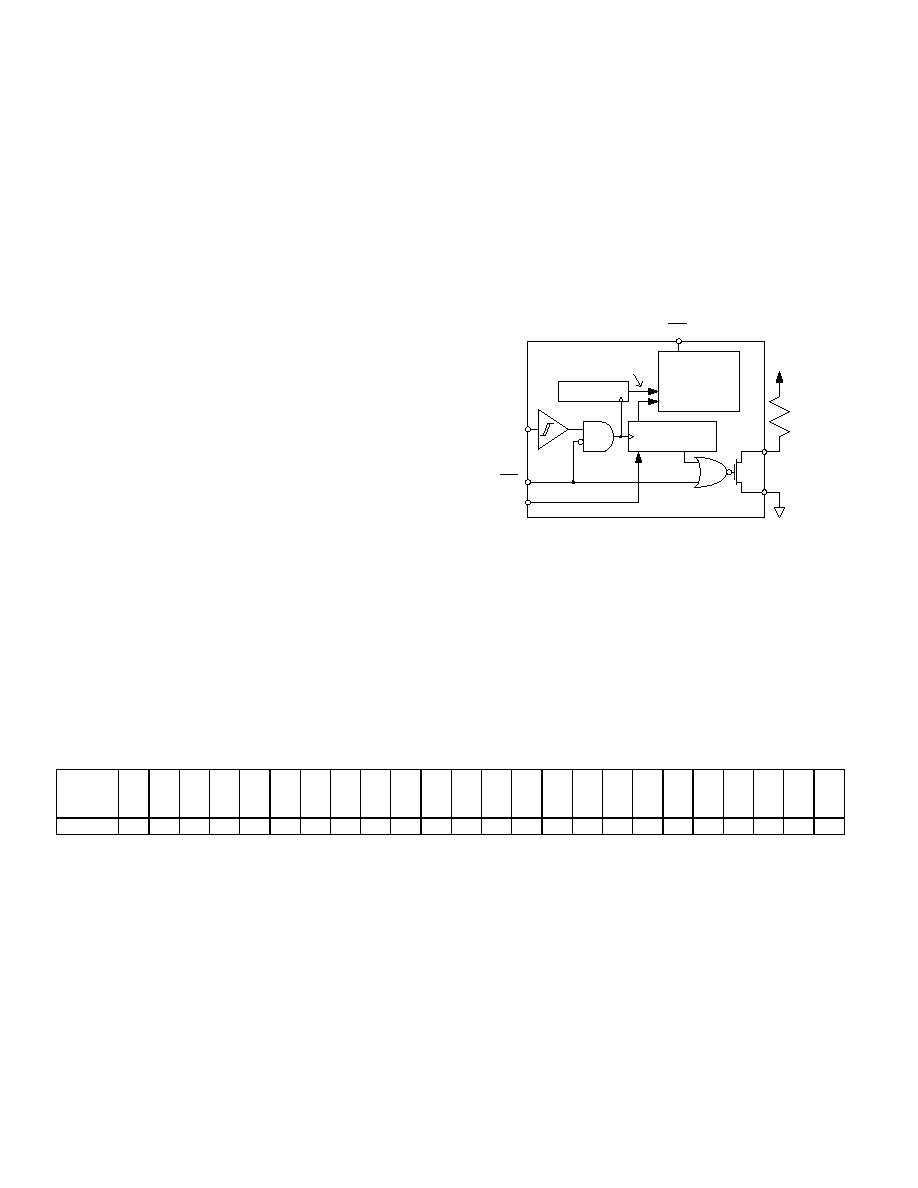
S E R IA L
R E G IS T E R
C O U N T E R
C O M M A N D
P R O C E S S O R
& A D D R E S S
D E C O D E
V A L ID
C O M M A N D
C S
C L K
S D I
R
P U L L U P
+ 5 V
S D O
G N D
P R
Figure 2. Equivalent Digital Input-Output Logic
The equivalent serial data input and output logic is shown in figure
2. The open drain output SDO is disabled whenever chip select
CS
is logic high. The SPI interface can be used in two slave modes
CPHA=1, CPOL=1 and CPHA=0, CPOL=0. CPHA and CPOL
refer to the control bits, which dictate SPI timing in the following
microprocessors/MicroConverters: ADuC812/824, M68HC11, and
MC68HC16R1/916R1.
Table 1. AD5235 24-bit Serial Data Word
M
S
B
L
S
B
AD5235
C3 C2 C1 C0 A3 A2 A1 A0 X X X X X X D9 D8 D7 D6 D5 D4 D3 D2 D1 D0
Command bits are identified as Cx, address bits are Ax, and data bits are Dx. Command instruction codes are defined in table 2.