 | –≠–ª–µ–∫—Ç—Ä–æ–Ω–Ω—ã–π –∫–æ–º–ø–æ–Ω–µ–Ω—Ç: AD534JH | –°–∫–∞—á–∞—Ç—å:  PDF PDF  ZIP ZIP |
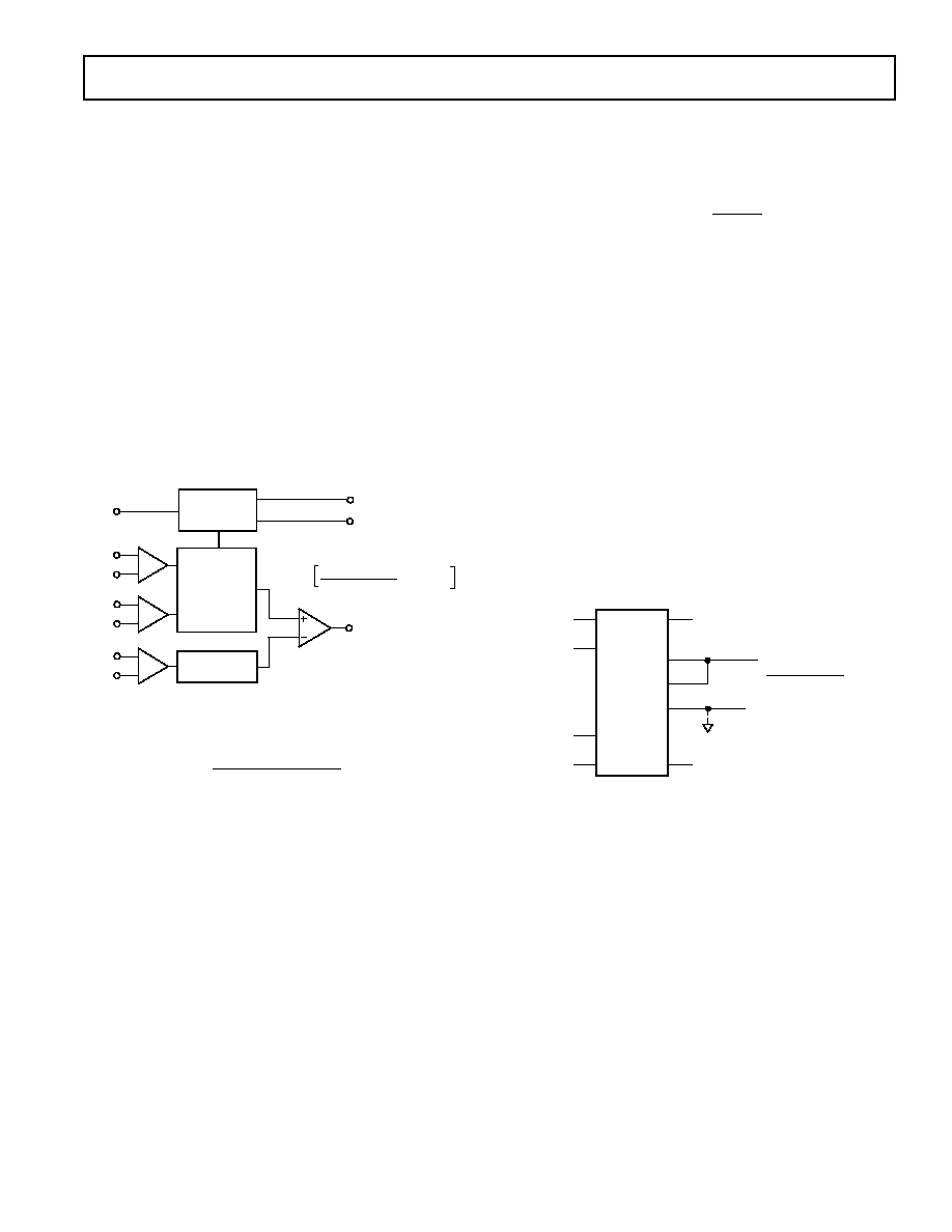
PIN CONFIGURATIONS
a
AD534
Internally Trimmed
Precision IC Multiplier
FEATURES
Pretrimmed to 0.25% max 4-Quadrant Error (AD534L)
All Inputs (X, Y and Z) Differential, High Impedance for
[(X
1
≠
X
2
) (Y
1
≠ Y
2
)/10 V] + Z
2
Transfer Function
Scale-Factor Adjustable to Provide up to X100 Gain
Low Noise Design: 90
V rms, 10 Hz≠10 kHz
Low Cost, Monolithic Construction
Excellent Long Term Stability
APPLICATIONS
High Quality Analog Signal Processing
Differential Ratio and Percentage Computations
Algebraic and Trigonometric Function Synthesis
Wideband, High-Crest rms-to-dc Conversion
Accurate Voltage Controlled Oscillators and Filters
Available in Chip Form
REV. B
Information furnished by Analog Devices is believed to be accurate and
reliable. However, no responsibility is assumed by Analog Devices for its
use, nor for any infringements of patents or other rights of third parties
which may result from its use. No license is granted by implication or
otherwise under any patent or patent rights of Analog Devices.
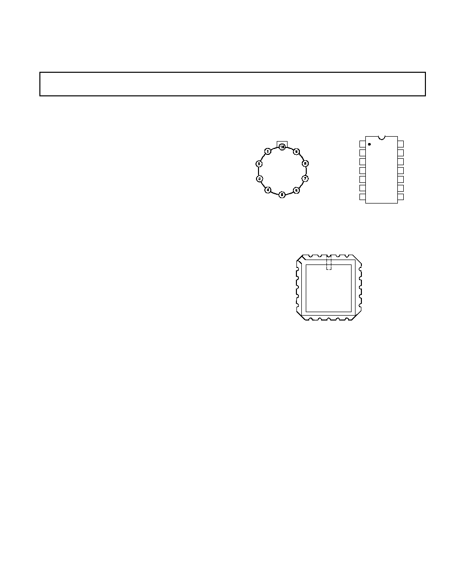
TO-116 (D-14)
Package
TOP VIEW
(Not to Scale)
14
13
12
11
10
9
8
1
2
3
4
5
6
7
NC = NO CONNECT
X1
+V
S
NC
AD534
OUT
Z1
Z2
NC
≠V
S
X2
NC
SF
NC
Y1
Y2
TO-100 (H-10A)
Package
≠V
S
+V
S
OUT
Z1
Z2
Y2
Y1
SF
X2
X1
AD534
TOP VIEW
(Not To Scale)
LCC (E-20A)
Package
+V
S
3
2
1
20 19
NC
X1
X2
NC
≠V
S
NC
Y2
Y1
NC
9
10
11 12
13
4
5
6
7
8
NC
NC
SF
NC
NC
18
17
16
15
14
OUT
NC
Z1
NC
Z2
AD534
TOP VIEW
(Not To Scale)
NC = NO CONNECT
PRODUCT DESCRIPTION
The AD534 is a monolithic laser trimmed four-quadrant multi-
plier divider having accuracy specifications previously found
only in expensive hybrid or modular products. A maximum
multiplication error of
±
0.25% is guaranteed for the AD534L
without any external trimming. Excellent supply rejection, low
temperature coefficients and long term stability of the on-chip
thin film resistors and buried Zener reference preserve accuracy
even under adverse conditions of use. It is the first multiplier to
offer fully differential, high impedance operation on all inputs,
including the Z-input, a feature which greatly increases its flex-
ibility and ease of use. The scale factor is pretrimmed to the
standard value of 10.00 V; by means of an external resistor, this
can be reduced to values as low as 3 V.
The wide spectrum of applications and the availability of several
grades commend this multiplier as the first choice for all new
designs. The AD534J (
±
1% max error), AD534K (
±
0.5% max)
and AD534L (
±
0.25% max) are specified for operation over the
0
∞
C to +70
∞
C temperature range. The AD534S (
±
1% max) and
AD534T (
±
0.5% max) are specified over the extended tempera-
ture range, ≠55
∞
C to +125
∞
C. All grades are available in her-
metically sealed TO-100 metal cans and TO-116 ceramic DIP
packages. AD534J, K, S and T chips are also available.
PROVIDES GAIN WITH LOW NOISE
The AD534 is the first general purpose multiplier capable of
providing gains up to X100, frequently eliminating the need for
separate instrumentation amplifiers to precondition the inputs.
The AD534 can be very effectively employed as a variable gain
differential input amplifier with high common-mode rejection.
The gain option is available in all modes, and will be found to
simplify the implementation of many function-fitting algorithms
such as those used to generate sine and tangent. The utility of
this feature is enhanced by the inherent low noise of the AD534:
90
µ
V, rms (depending on the gain), a factor of 10 lower than
previous monolithic multipliers. Drift and feedthrough are also
substantially reduced over earlier designs.
UNPRECEDENTED FLEXIBILITY
The precise calibration and differential Z-input provide a degree
of flexibility found in no other currently available multiplier.
Standard MDSSR functions (multiplication, division, squaring,
square-rooting) are easily implemented while the restriction to
particular input/output polarities imposed by earlier designs has
been eliminated. Signals may be summed into the output, with
or without gain and with either a positive or negative sense.
Many new modes based on implicit-function synthesis have
been made possible, usually requiring only external passive
components. The output can be in the form of a current, if
desired, facilitating such operations as integration.
One Technology Way, P.O. Box 9106, Norwood, MA 02062-9106, U.S.A.
Tel: 781/329-4700
World Wide Web Site: http://www.analog.com
Fax: 781/326-8703
© Analog Devices, Inc., 1999
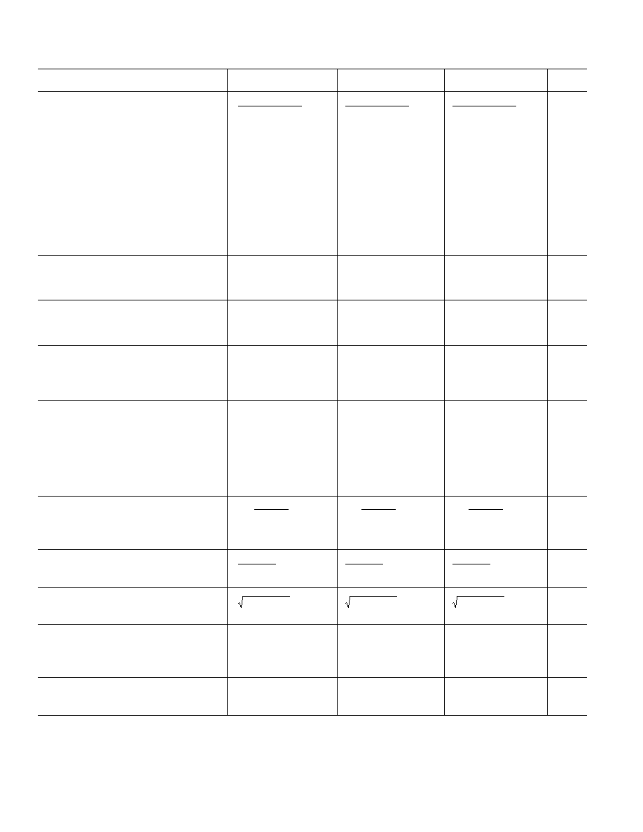
AD534≠SPECIFICATIONS
Model
AD534J
AD534K
AD534L
Min
Typ
Max
Min
Typ
Max
Min
Typ
Max
Units
MULTIPLIER PERFORMANCE
Transfer Function
( X
1
≠ X
2
)(Y
1
≠ Y
2
)
10 V
+
Z
2
( X
1
≠ X
2
)(Y
1
≠ Y
2
)
10 V
+
Z
2
( X
1
≠ X
2
)(Y
1
≠ Y
2
)
10 V
+
Z
2
Total Error
1
(≠10 V
X, Y
+10 V)
1.0
0.5
0.25
%
T
A
= min to max
±
1.5
±
1.0
±
0.5
%
Total Error vs. Temperature
±
0.022
±
0.015
±
0.008
%/
∞
C
Scale Factor Error
(SF = 10.000 V Nominal)
2
±
0.25
±
0.1
±
0.1
%
Temperature-Coefficient of
Scaling Voltage
±
0.02
±
0.01
±
0.005
%/
∞
C
Supply Rejection (
±
15 V
±
1 V)
±
0.01
±
0.01
±
0.01
%
Nonlinearity, X (X = 20 V p-p, Y = 10 V)
±
0.4
±
0.2
0.3
±
0.10
0.12
%
Nonlinearity, Y (Y = 20 V p-p, X = 10 V)
±
0.2
±
0.1
0.1
±
0.005
0.1
%
Feedthrough
3
, X (Y Nulled,
X = 20 V p-p 50 Hz)
±
0.3
±
0.15
0.3
±
0.05
0.12
%
Feedthrough
3
, Y (X Nulled,
Y = 20 V p-p 50 Hz)
±
0.01
±
0.01
0.1
±
0.003
0.1
%
Output Offset Voltage
±
5
30
±
2
15
±
2
10
mV
Output Offset Voltage Drift
200
100
100
µ
V/
∞
C
DYNAMICS
Small Signal BW (V
OUT
= 0.1 rms)
1
1
1
MHz
1% Amplitude Error (C
LOAD
= 1000 pF)
50
50
50
kHz
Slew Rate (V
OUT
20 p-p)
20
20
20
V/
µ
s
Settling Time (to 1%,
V
OUT
= 20 V)
2
2
2
µ
s
NOISE
Noise Spectral-Density SF = 10 V
0.8
0.8
0.8
µ
V/
Hz
SF = 3 V
4
0.4
0.4
0.4
µ
V/
Hz
Wideband Noise f = 10 Hz to 5 MHz
1
1
1
mV/rms
Wideband Noise
f = 10 Hz to 10 kHz
90
90
90
µ
V/rms
OUTPUT
Output Voltage Swing
11
11
11
V
Output Impedance (f
1 kHz)
0.1
0.1
0.1
Output Short Circuit Current
(R
L
= 0, T
A
= min to max)
30
30
30
mA
Amplifier Open Loop Gain (f = 50 Hz)
70
70
70
dB
INPUT AMPLIFIERS (X, Y and Z)
5
Signal Voltage Range (Diff. or CM
±
10
±
10
±
10
V
Operating Diff.)
±
12
±
12
±
12
V
Offset Voltage X, Y
±
5
20
±
2
10
±
2
10
mV
Offset Voltage Drift X, Y
100
50
50
µ
V/
∞
C
Offset Voltage Z
±
5
30
±
2
15
±
2
±
10
mV
Offset Voltage Drift Z
200
100
100
µ
V/
∞
C
CMRR
60
80
70
90
70
90
dB
Bias Current
0.8
2.0
0.8
2.0
0.8
2.0
µ
A
Offset Current
0.1
0.1
0.05
0.2
µ
A
Differential Resistance
10
10
10
M
DIVIDER PERFORMANCE
Transfer Function (X
1
> X
2
)
10 V
( Z
2
-
Z
1
)
( X
1
-
X
2
)
+
Y
1
10 V
( Z
2
-
Z
1
)
( X
1
-
X
2
)
+
Y
1
10 V
( Z
2
-
Z
1
)
( X
1
-
X
2
)
+
Y
1
Total Error
1
(X = 10 V, ≠10 V
Z
+10 V)
±
0.75
±
0.35
±
0.2
%
(X = 1 V, ≠1 V
Z
+1 V)
±
2.0
±
1.0
±
0.8
%
(0.1 V
X
10 V, ≠10 V
Z
10 V)
±
2.5
±
1.0
±
0.8
%
SQUARE PERFORMANCE
Transfer Function
( X
1
-
X
2
)
2
10 V
+
Z
2
( X
1
-
X
2
)
2
10 V
+
Z
2
( X
1
-
X
2
)
2
10 V
+
Z
2
Total Error (≠10 V
X
10 V)
±
0.6
±
0.3
±
0.2
%
SQUARE-ROOTER PERFORMANCE
Transfer Function (Z
1
Z
2
)
10 V ( Z
2
-
Z
1
)
+
X
2
10 V ( Z
2
-
Z
1
)
+
X
2
10 V ( Z
2
-
Z
1
)
+
X
2
Total Error
1
(1 V
Z
10 V)
±
1.0
±
0.5
±
0.25
%
POWER SUPPLY SPECIFICATIONS
Supply Voltage
Rated Performance
±
15
±
15
±
15
V
Operating
±
8
18
±
8
18
±
8
18
V
Supply Current
Quiescent
4
6
4
6
4
6
mA
PACKAGE OPTIONS
TO-100 (H-10A)
AD534JH
AD534KH
AD534LH
TO-116 (D-14)
AD534JD
AD534KD
AD534LD
Chips
AD534K Chips
(@ T
A
= + 25 C, V
S
= 15 V, R
2 k )
N
OTES
1
Figures given are percent of full scale,
±
10 V (i.e., 0.01% = 1 mV).
2
May be reduced down to 3 V using external resistor between ≠V
S
and SF.
3
Irreducible component due to nonlinearity: excludes effect of offsets.
4
Using external resistor adjusted to give SF = 3 V.
5
See Functional Block Diagram for definition of sections.
Specifications subject to change without notic
e.
Specifications shown in boldface are tested on all production units at final electrical
test. Results from those tests are used to calculate outgoing quality levels. All min and
max specifications are guaranteed, although only those shown in boldface are tested
on all production units.
REV. B
≠2≠
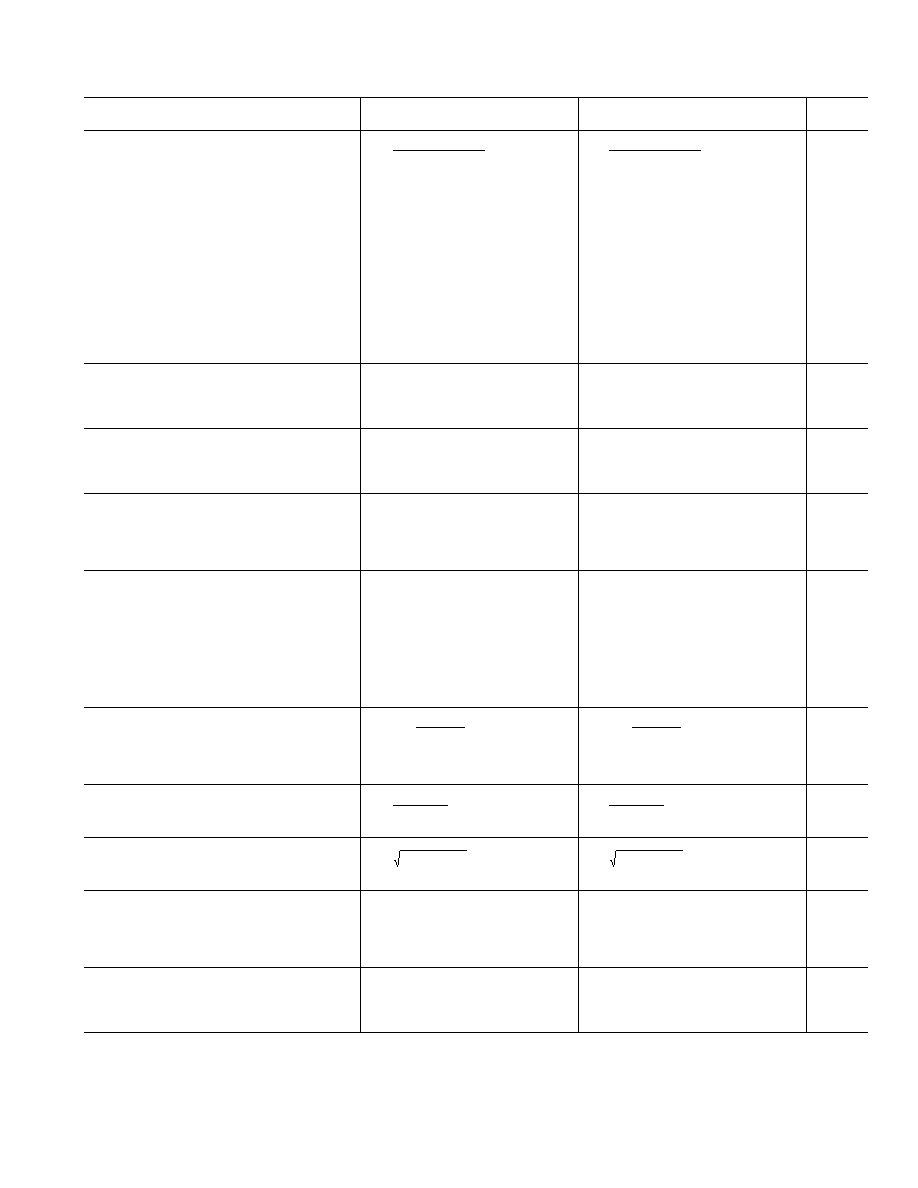
Model
AD534S
AD534T
Min
Typ
Max
Min
Typ
Max
Units
MULTIPLIER PERFORMANCE
Transfer Function
( X
1
≠ X
2
)(Y
1
≠ Y
2
)
10 V
+
Z
2
( X
1
≠ X
2
)(Y
1
≠ Y
2
)
10 V
+
Z
2
Total Error
1
(≠10 V
X, Y
+10 V)
1.0
0.5
%
T
A
= min to max
2.0
±
1.0
%
Total Error vs. Temperature
0.02
0.01
%/
∞
C
Scale Factor Error
(SF = 10.000 V Nominal)
2
±
0.25
±
0.1
%
Temperature-Coefficient of
Scaling Voltage
±
0.02
0.005
%/
∞
C
Supply Rejection (
±
15 V
±
1 V)
±
0.01
±
0.01
%
Nonlinearity, X (X = 20 V p-p, Y = 10 V)
±
0.4
±
0.2
0.3
%
Nonlinearity, Y (Y = 20 V p-p, X = 10 V)
±
0.2
±
0.1
0.1
%
Feedthrough
3
, X (Y Nulled,
X = 20 V p-p 50 Hz)
±
0.3
±
0.15
0.3
%
Feedthrough
3
, Y (X Nulled,
Y = 20 V p-p 50 Hz)
±
0.01
±
0.01
0.1
%
Output Offset Voltage
±
5
±
30
±
2
15
mV
Output Offset Voltage Drift
500
300
µ
V/
∞
C
DYNAMICS
Small Signal BW (V
OUT
= 0.1 rms)
1
1
MHz
1% Amplitude Error (C
LOAD
= 1000 pF)
50
50
kHz
Slew Rate (V
OUT
20 p-p)
20
20
V/
µ
s
Settling Time (to 1%,
V
OUT
= 20 V)
2
2
µ
s
NOISE
Noise Spectral-Density SF = 10 V
0.8
0.8
µ
V/
Hz
SF = 3 V
4
0.4
0.4
µ
V/
Hz
Wideband Noise f = 10 Hz to 5 MHz
1.0
1.0
mV/rms
Wideband Noise
f = 10 Hz to 10 kHz
90
90
µ
V/rms
OUTPUT
Output Voltage Swing
±
11
±
11
V
Output Impedance (f
1 kHz)
0.1
0.1
Output Short Circuit Current
(R
L
= 0, T
A
= min to max)
30
30
mA
Amplifier Open Loop Gain (f = 50 Hz)
70
70
dB
INPUT AMPLIFIERS (X, Y and Z)
5
Signal Voltage Range (Diff. or CM
±
10
±
10
V
Operating Diff.)
±
12
±
12
V
Offset Voltage X, Y
±
5
20
±
2
10
mV
Offset Voltage Drift X, Y
100
150
µ
V/
∞
C
Offset Voltage Z
±
5
30
±
2
15
mV
Offset Voltage Drift Z
500
300
µ
V/
∞
C
CMRR
60
80
70
90
dB
Bias Current
0.8
2.0
0.8
2.0
µ
A
Offset Current
0.1
0.1
µ
A
Differential Resistance
10
10
M
DIVIDER PERFORMANCE
Transfer Function (X
1
> X
2
)
10 V
( Z
2
-
Z
1
)
( X
1
-
X
2
)
+
Y
1
10 V
( Z
2
-
Z
1
)
( X
1
-
X
2
)
+
Y
1
Total Error
1
(X = 10 V, ≠10 V
Z
+10 V)
±
0.75
±
0.35
%
(X = 1 V, ≠1 V
Z
+1 V)
±
2.0
±
1.0
%
(0.1 V
X
10 V, ≠10 V
Z
10 V)
±
2.5
±
1.0
%
SQUARE PERFORMANCE
Transfer Function
( X
1
-
X
2
)
2
10 V
+
Z
2
( X
1
-
X
2
)
2
10 V
+
Z
2
Total Error (≠10 V
X
10 V)
±
0.6
±
0.3
%
SQUARE-ROOTER PERFORMANCE
Transfer Function (Z
1
Z
2
)
10 V ( Z
2
-
Z
1
)
+
X
2
10 V ( Z
2
-
Z
1
)
+
X
2
Total Error
1
(1 V
Z
10 V)
±
1.0
±
0.5
%
POWER SUPPLY SPECIFICATIONS
Supply Voltage
Rated Performance
±
15
±
15
V
Operating
±
8
22
±
8
22
V
Supply Current
Quiescent
4
6
4
6
mA
PACKAGE OPTIONS
TO-100 (H-10A)
AD534SH
AD534TH
TO-116 (D-14)
AD534SD
AD534TD
E-20A
AD534SE
Chips
AD534S Chips
AD534T Chips
AD534
N
OTES
1
Figures given are percent of full scale,
±
10 V (i.e., 0.01% = 1 mV).
2
May be reduced down to 3 V using external resistor between ≠V
S
and SF.
3
Irreducible component due to nonlinearity: excludes effect of offsets.
4
Using external resistor adjusted to give SF = 3 V.
5
See Functional Block Diagram for definition of sections.
Specifications subject to change without notice.
REV. B
≠3≠
S
pecifications shown in boldface are tested on all production units at final electrical
test. Results from those tests are used to calculate outgoing quality levels. All min and
max specifications are guaranteed, although only those shown in boldface are tested
on all production units.
AD534
≠4≠
REV. B
ABSOLUTE MAXIMUM RATINGS
AD534J, K, L
AD534S, T
Supply Voltage
±
18 V
±
22 V
Internal Power Dissipation
500 mW
*
Output Short-Circuit to Ground
Indefinite
*
Input Voltages, X
1
X
2
Y
1
Y
2
Z
1
Z
2
±
V
S
*
Rated Operating Temperature Range
0
∞
C to +70
∞
C
≠55
∞
C to
+125
∞
C
Storage Temperature Range
≠65
∞
C to +150
∞
C
*
Lead Temperature Range, 60 s Soldering
+300
∞
C
*
*Same as AD534J Specs.
ORDERING GUIDE
Model
Temperature Range
Package Description
Package Option
AD534JD
0
∞
C to +70
∞
C
Side Brazed DIP
D-14
AD534KD
0
∞
C to +70
∞
C
Side Brazed DIP
D-14
AD534LD
0
∞
C to +70
∞
C
Side Brazed DIP
D-14
AD534JH
0
∞
C to +70
∞
C
Header
H-10A
AD534JH/+
0
∞
C to +70
∞
C
Header
H-10A
AD534KH
0
∞
C to +70
∞
C
Header
H-10A
AD534KH/+
0
∞
C to +70
∞
C
Header
H-10A
AD534LH
0
∞
C to +70
∞
C
Header
H-10A
AD534K Chip
0
∞
C to +70
∞
C
Chip
AD534SD
≠55
∞
C to +125
∞
C
Side Brazed DIP
D-14
AD534SD/883B
≠55
∞
C to +125
∞
C
Side Brazed DIP
D-14
AD534TD
≠55
∞
C to +125
∞
C
Side Brazed DIP
D-14
AD534TD/883B
≠55
∞
C to +125
∞
C
Side Brazed DIP
D-14
JM38510/13902BCA
≠55
∞
C to +125
∞
C
Side Brazed DIP
D-14
JM38510/13901BCA
≠55
∞
C to +125
∞
C
Side Brazed DIP
D-14
AD534SE
≠55
∞
C to +125
∞
C
LCC
E-20A
AD534SE/883B
≠55
∞
C to +125
∞
C
LCC
E-20A
AD534TE/883B
≠55
∞
C to +125
∞
C
LCC
E-20A
AD534SH
≠55
∞
C to +125
∞
C
Header
H-10A
AD534SH/883B
≠55
∞
C to +125
∞
C
Header
H-10A
AD534TH
≠55
∞
C to +125
∞
C
Header
H-10A
AD534TH/883B
≠55
∞
C to +125
∞
C
Header
H-10A
JM38510/13902BIA
≠55
∞
C to +125
∞
C
Header
H-10A
JM38510/13901BIA
≠55
∞
C to +125
∞
C
Header
H-10A
AD534S Chip
≠55
∞
C to +125
∞
C
Chip
AD534T Chip
≠55
∞
C to +125
∞
C
Chip
The
rmal C
haracteristics
Thermal Resistance
JC
= 25
∞
C/W for H-10A
JA
= 150
∞
C/W for H-10A
JC
= 25
∞
C/W for D-14 or E-20A
JA
= 95
∞
C/W for D-14 or E-20A
X
1
+V
S
OUT
Y
2
≠V
S
Z
2
Y
1
SF
X
2
Z
1
THE AD534 IS AVAILABLE IN LASER - TRIMMED CHIP FORM
0.076
(1.93)
0.100 (2.54)
CHIP DIMENSIONS AND BONDING DIAGRAM
Dimensions shown in inches and (mm).
Contact factory for latest dimensions.
470k
50k
1k
TO APPROPRIATE
INPUT TERMINAL
+V
S
≠V
S
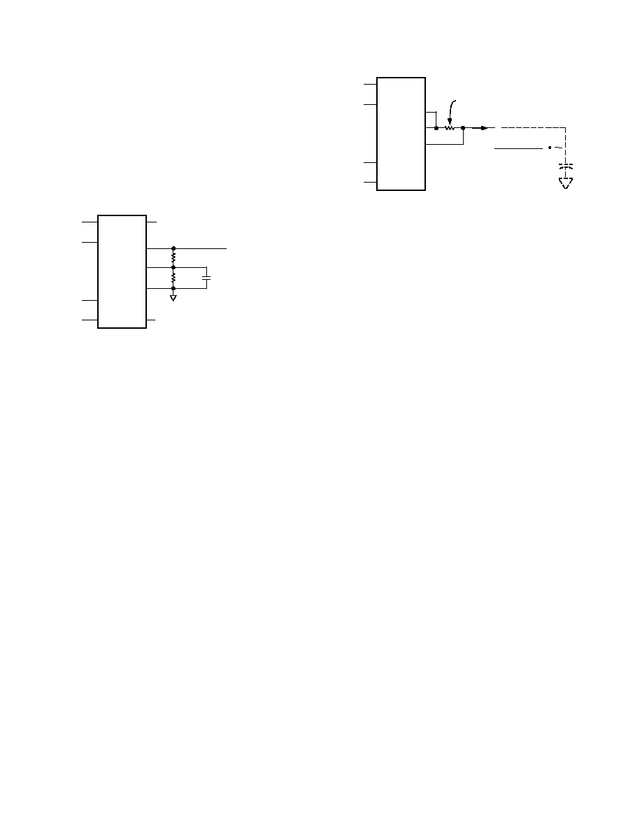
Figure 1. Optional Trimming Configuration
CAUTION
ESD (electrostatic discharge) sensitive device. Electrostatic charges as high as 4000 V readily
accumulate on the human body and test equipment and can discharge without detection.
Although the AD534 features proprietary ESD protection circuitry, permanent damage may
occur on devices subjected to high energy electrostatic discharges. Therefore, proper ESD
precautions are recommended to avoid performance degradation or loss of functionality.
WARNING!
ESD SENSITIVE DEVICE
AD534
REV. B
≠5≠
FUNCTIONAL DESCRIPTION
Figure 2 is a functional block diagram of the AD534. Inputs are
converted to differential currents by three identical voltage-to-
current converters, each trimmed for zero offset. The product
of the X and Y currents is generated by a multiplier cell using
Gilbert's translinear technique. An on-chip "Buried Zener"
provides a highly stable reference, which is laser trimmed to
provide an overall scale factor of 10 V. The difference between
XY/SF and Z is then applied to the high gain output amplifier.
This permits various closed loop configurations and dramati-
cally reduces nonlinearities due to the input amplifiers, a domi-
nant source of distortion in earlier designs. The effectiveness of
the new scheme can be judged from the fact that under typical
conditions as a multiplier the nonlinearity on the Y input, with
X at full scale (
±
10 V), is
±
0.005% of FS; even at its worst
point, which occurs when X =
±
6.4 V, it is typically only
±
0.05% of FS Nonlinearity for signals applied to the X input,
on the other hand, is determined almost entirely by the multi-
plier element and is parabolic in form. This error is a major
factor in determining the overall accuracy of the unit and hence
is closely related to the device grade.
V-1
X
1
X
2
V-1
Y
1
Y
2
V-1
Z
1
Z
2
SF
AD534
+V
S
≠V
S
A
OUT
TRANSFER FUNCTION
V
O
= A ≠ (Z
1
≠ Z
2
)
(X
1
≠ X
2
) (Y
1
≠ Y
2
)
SF
HIGH GAIN
OUTPUT
AMPLIFIER
+
≠
+
≠
+
≠
STABLE
REFERENCE
AND BIAS
TRANSLINEAR
MULTIPLIER
ELEMENT
0.75 ATTEN
Figure 2. Functional Block Diagram
The generalized transfer function for the AD534 is given by:
V
OUT
=
A
( X
1
-
X
2
) (Y
1
-
Y
2
)
SF
-
( Z
1
-
Z
2
)
where A = open loop gain of output amplifier, typically
70 dB at dc
X, Y, Z = input voltages (full scale =
±
SF, peak =
±
1.25 SF)
SF = scale factor, pretrimmed to 10.00 V but adjustable
by the user down to 3 V.
In most cases the open loop gain can be regarded as infinite,
and SF will be 10 V. The operation performed by the AD534,
can then be described in terms of equation:
( X
1
-
X
2
) (Y
1
-
Y
2
)
=
10 V ( Z
1
-
Z
2
)
The user may adjust SF for values between 10.00 V and 3 V by
connecting an external resistor in series with a potentiometer
between SF and ≠V
S
. The approximate value of the total resis-
tance for a given value of SF is given by the relationship:
R
SF
=
5.4K
SF
10
-
SF
Due to device tolerances, allowance should be made to vary R
SF
;
by
±
25% using the potentiometer. Considerable reduction in
bias currents, noise and drift can be achieved by decreasing SF.
This has the overall effect of increasing signal gain without the
customary increase in noise. Note that the peak input signal is
always limited to 1.25 SF (i.e.,
±
5 V for SF = 4 V) so the overall
transfer function will show a maximum gain of 1.25. The per-
formance with small input signals, however, is improved by
using a lower SF since the dynamic range of the inputs is now
fully utilized. Bandwidth is unaffected by the use of this option.
Supply voltages of
±
15 V are generally assumed. However,
satisfactory operation is possible down to
±
8 V (see Figure 16).
Since all inputs maintain a constant peak input capability of
±
1.25 SF some feedback attenuation will be necessary to
achieve output voltage swings in excess of
±
12 V when using
higher supply voltages.
OPERATION AS A MULTIPLIER
Figure 3 shows the basic connection for multiplication. Note
that the circuit will meet all specifications without trimming.
X
1
X
2
Y
1
Y
2
Z
1
Z
2
AD534
= + Z
2
(X
1
≠ X
2
) (Y
1
≠ Y
2
)
10V
OUTPUT , 12V PK
X INPUT
10V FS
12V PK
Y INPUT
10V FS
12V PK
+15V
OUT
≠V
S
+V
S
≠15V
OPTIONAL SUMMING
INPUT, Z, 10V PK
SF
Figure 3. Basic Multiplier Connection
In some cases the user may wish to reduce ac feedthrough to a
minimum (as in a suppressed carrier modulator) by applying an
external trim voltage (
±
30 mV range required) to the X or Y
input (see Figure 1). Figure 19 shows the typical ac feedthrough
with this adjustment mode. Note that the Y input is a factor of
10 lower than the X input and should be used in applications
where null suppression is critical.
The high impedance Z
2
terminal of the AD534 may be used to
sum an additional signal into the output. In this mode the out-
put amplifier behaves as a voltage follower with a 1 MHz small
signal bandwidth and a 20 V/
µ
s slew rate. This terminal should
always be referenced to the ground point of the driven system,
particularly if this is remote. Likewise, the differential inputs
should be referenced to their respective ground potentials to
realize the full accuracy of the AD534.
AD534
≠6≠
REV. B
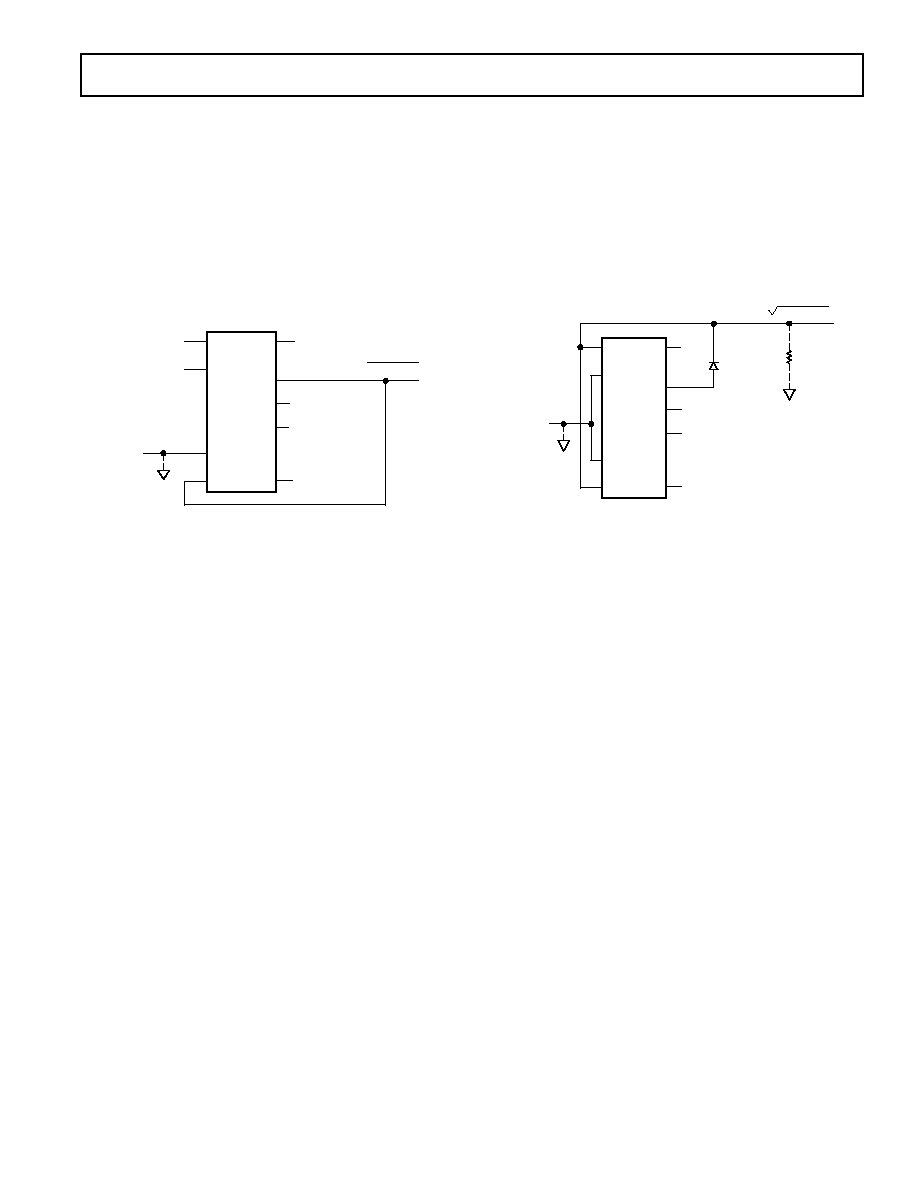
A much lower scaling voltage can be achieved without any re-
duction of input signal range using a feedback attenuator as
shown in Figure 4. In this example, the scale is such that V
OUT
= XY, so that the circuit can exhibit a maximum gain of 10.
This connection results in a reduction of bandwidth to about
80 kHz without the peaking capacitor C
F
= 200 pF. In addition,
the output offset voltage is increased by a factor of 10 making
external adjustments necessary in some applications. Adjust-
ment is made by connecting a 4.7 M
resistor between Z
1
and
the slider of a pot connected across the supplies to provide
±
300 mV of trim range at the output.
X
1
X
2
Y
1
Y
2
Z
1
Z
2
AD534
X INPUT
10V FS
12V PK
Y INPUT
10V FS
12V PK
+15V
OUT
≠V
S
+V
S
≠15V
OPTIONAL
PEAKING
CAPACITOR
C
F
= 200pF
90k
10k
SF
OUTPUT , 12V PK
= (X
1
≠ X
2
) (Y
1
≠ Y
2
)
(SCALE = 1V)
Figure 4. Connections for Scale-Factor of Unity
Feedback attenuation also retains the capability for adding a
signal to the output. Signals may be applied to the high imped-
ance Z
2
terminal where they are amplified by +10 or to the
common ground connection where they are amplified by +1.
Input signals may also be applied to the lower end of the 10 k
resistor, giving a gain of ≠9. Other values of feedback ratio, up
to X100, can be used to combine multiplication with gain.
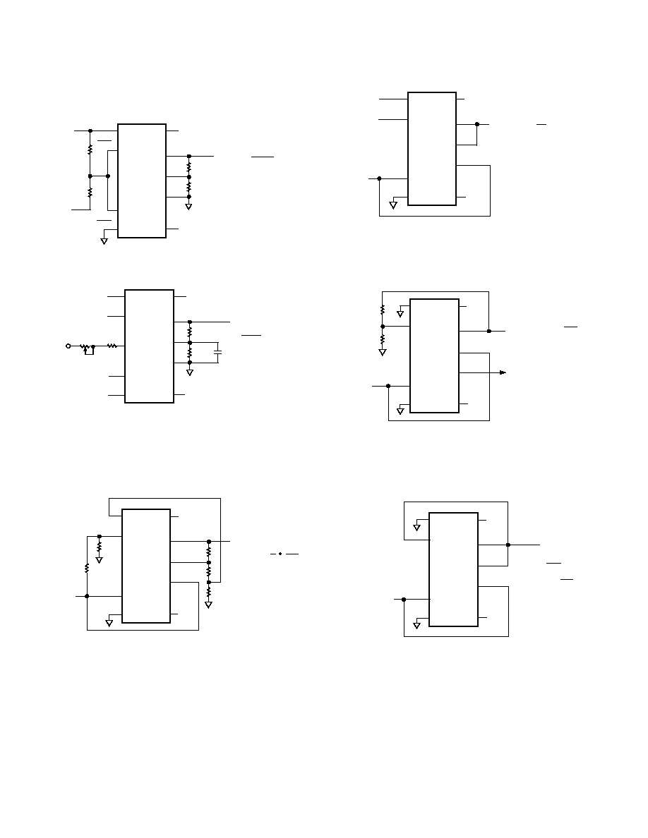
Occasionally it may be desirable to convert the output to a cur-
rent, into a load of unspecified impedance or dc level. For ex-
ample, the function of multiplication is sometimes followed by
integration; if the output is in the form of a current, a simple
capacitor will provide the integration function. Figure 5 shows
how this can be achieved. This method can also be applied in
squaring, dividing and square rooting modes by appropriate
choice of terminals. This technique is used in the voltage-
controlled low-pass filter and the differential-input voltage-to-
frequency converter shown in the Applications section.
X
1
X
2
Y
1
Y
2
Z
1
Z
2
AD534
1
RS
(X
1
≠ X
2
) (Y
1
≠ Y
2
)
I
OUT
=
10V
INTEGRATOR
CAPACITOR
(SEE TEXT)
X INPUT
10V FS
12V PK
Y INPUT
10V FS
12V PK
OUT
≠V
S
+V
S
CURRENT-SENSING
RESISTOR, R
S
, 2k MIN
SF
Figure 5. Conversion of Output to Current
OPERATION AS A SQUARER
Operation as a squarer is achieved in the same fashion as the
multiplier except that the X and Y inputs are used in parallel.
The differential inputs can be used to determine the output
polarity (positive for X
1
= Y
l
and X
2
= Y
2
, negative if either one
of the inputs is reversed). Accuracy in the squaring mode is
typically a factor of 2 better than in the multiplying mode, the
largest errors occurring with small values of output for input
below 1 V.
If the application depends on accurate operation for inputs that
are always less than
±
3 V, the use of a reduced value of SF is
recommended as described in the Functional Description sec-
tion (previous page). Alternatively, a feedback attenuator may
be used to raise the output level. This is put to use in the differ-
ence-of-squares application to compensate for the factor of 2
loss involved in generating the sum term (see Figure 8).
The difference-of-squares function is also used as the basis for a
novel rms-to-dc converter shown in Figure 15. The averaging
filter is a true integrator, and the loop seeks to zero its input.
For this to occur, (V
IN
)
2
≠ (V
OUT
)
2
= 0 (for signals whose period
is well below the averaging time-constant). Hence V
OUT
is
forced to equal the rms value of V
IN
. The absolute accuracy of
this technique is very high; at medium frequencies, and for
signals near full scale, it is determined almost entirely by the
ratio of the resistors in the inverting amplifier. The multiplier
scaling voltage affects only open loop gain. The data shown is
typical of performance that can be achieved with an AD534K,
but even using an AD534J, this technique can readily provide
better than 1% accuracy over a wide frequency range, even for
crest-factors in excess of 10.
AD534
REV. B
≠7≠
OPERATION AS A DIVIDER
The AD535, a pin-for-pin functional equivalent to the AD534,
has guaranteed performance in the divider and square-rooter
configurations and is recommended for such applications.
Figure 6 shows the connection required for division. Unlike
earlier products, the AD534 provides differential operation on
both numerator and denominator, allowing the ratio of two
floating variables to be generated. Further flexibility results from
access to a high impedance summing input to Y
1
. As with all
dividers based on the use of a multiplier in a feedback loop, the
bandwidth is proportional to the denominator magnitude, as
shown in Figure 23.
X
1
X
2
Y
1
Y
2
Z
1
Z
2
AD534
10V (Z
2
≠ Z
1
)
=
(X
1
≠ X
2
)
OUTPUT, 12V PK
+ Y
1
Z INPUT
(NUMERATOR)
10V FS, 12V PK
X INPUT
(DENOMINATOR)
+10V FS
+12V PK
OPTIONAL
SUMMING
INPUT
10V PK
OUT
≠V
S
+V
S
SF
+
≠
+15V
≠15V
Figure 6. Basic Divider Connection
Without additional trimming, the accuracy of the AD534K
and L is sufficient to maintain a 1% error over a 10 V to 1 V
denominator range. This range may be extended to 100:1 by
simply reducing the X offset with an externally generated trim
voltage (range required is
±
3.5 mV max) applied to the unused
X input (see Figure 1). To trim, apply a ramp of +100 mV to
+V at 100 Hz to both X
1
and Z
1
(if X
2
is used for offset adjust-
ment, otherwise reverse the signal polarity) and adjust the trim
voltage to minimize the variation in the output.*
Since the output will be near +10 V, it should be ac-coupled for
this adjustment. The increase in noise level and reduction in
bandwidth preclude operation much beyond a ratio of 100 to 1.
As with the multiplier connection, overall gain can be intro-
duced by inserting a simple attenuator between the output and
Y
2
terminal. This option, and the differential-ratio capability of
the AD534 are utilized in the percentage-computer application
shown in Figure 12. This configuration generates an output
proportional to the percentage deviation of one variable (A) with
respect to a reference variable (B), with a scale of one volt per
percent.
OPERATION AS A SQUARE ROOTER
The operation of the AD534 in the square root mode is shown
in Figure 7. The diode prevents a latching condition which
could occur if the input momentarily changes polarity. As
shown, the output is always positive; it may be changed to a
negative output by reversing the diode direction and interchang-
ing the X inputs. Since the signal input is differential, all combi-
nations of input and output polarities can be realized, but
operation is restricted to the one quadrant associated with each
combination of inputs.
X
1
X
2
Y
1
Y
2
Z
1
Z
2
AD534
OUTPUT, 12V PK
10V (Z
2
≠ Z
1
) +X
2
=
Z INPUT
10V FS
12V PK
OPTIONAL
SUMMING
INPUT,
X, 10V PK
OUT
≠V
S
+V
S
SF
+15V
≠15V
REVERSE
THIS AND X
INPUTS FOR
NEGATIVE
OUTPUTS
R
L
(MUST BE
PROVIDED)
+
≠
Figure 7. Square-Rooter Connection
In contrast to earlier devices, which were intolerant of capacitive
loads in the square root modes, the AD534 is stable with all
loads up to at least 1000 pF. For critical applications, a small
adjustment to the Z input offset (see Figure 1) will improve
accuracy for inputs below 1 V.
*See the AD535 data sheet for more details.
AD534≠Applications Section
≠8≠
The versatility of the AD534 allows the creative designer to
implement a variety of circuits such as wattmeters, frequency
doublers and automatic gain controls to name but a few.
X
1
X
2
Y
1
Y
2
Z
1
Z
2
AD534
OUTPUT =
A
2
≠ B
2
10V
OUT
≠V
S
+V
S
SF
+15V
≠15V
A ≠ B
2
A
B
A + B
2
30k
10k
Figure 8. Difference-of-Squares
X
1
X
2
Y
1
Y
2
Z
1
Z
2
AD534
OUTPUT, 12V PK
=
E
C
E
S
0.1V
OUT
≠V
S
+V
S
SF
+15V
≠15V
SIGNAL INPUT,
E
S
, 5V PK
39k
1k
0.005 F
≠V
S
CONTROL INPUT,
E
C
, ZERO TO 5V
SET
GAIN
1k
2k
NOTES:
1) GAIN IS X 10 PER-VOLT OF E
C
, ZERO TO X 50
2) WIDEBAND (10Hz ≠ 30kHz) OUTPUT NOISE IS 3mV RMS, TYP
CORRESPONDING TO A.F.S. S/N RATIO OF 70dB
3) NOISE REFERRED TO SIGNAL INPUT, WITH E
C
= 5V, IS 60 V RMS, TYP
4) BANDWITH IS DC TO 20kHz, ≠3dB, INDEPENDENT OF GAIN
Figure 9. Voltage-Controlled Amplifier
X
1
X
2
Y
1
Y
2
Z
1
Z
2
AD534
OUTPUT = (10V) sin
OUT
≠V
S
+V
S
SF
+15V
≠15V
4.7k
4.3k
18k
10k
USING CLOSE TOLERANCE RESISTORS AND AD534L, ACCURACY
OF FIT IS WITHIN 0.5% AT ALL POINTS. IS IN RADIANS.
INPUT, E
0 TO +10V
WHERE =
E
2 10V
3k
Figure 10. Sine-Function Generator
X
1
X
2
Y
1
Y
2
Z
1
Z
2
OUTPUT = 1 E
C
sin t
10V
E
M
OUT
≠V
S
+V
S
SF
+15V
≠15V
THE SF PIN OR A Z-ATTENUATOR CAN BE USED TO PROVIDE OVERALL
SIGNAL AMPLIFICATION, OPERATION FROM A SINGLE SUPPLY POSSIBLE;
BIAS Y
2
TO V
S
/2.
CARRIER
INPUT
E
C
sin t
MODULATION
INPUT, E
M
AD534
Figure 11. Linear AM Modulator
9k
1k
X
1
X
2
Y
1
Y
2
Z
2
Z
1
AD534
OUTPUT = (100V)
B
A ≠ B
(1% PER VOLT)
OUT
≠V
S
+V
S
SF
+15V
≠15V
OTHER SCALES, FROM 10% PER VOLT TO 0.1% PER VOLT
CAN BE OBTAINED BY ALTERING THE FEEDBACK RATIO.
B INPUT
(+V
E
ONLY)
A INPUT
( )
Figure 12. Percentage Computer
X
1
X
2
Y
1
Y
2
Z
1
Z
2
OUTPUT, 5V/PK
= (10V)
1 + y
y
(10V)
Y
WHERE y =
OUT
≠V
S
+V
S
SF
+15V
≠15V
INPUT, Y 10V FS
AD534
Figure 13. Bridge-Linearization Function
AD534
REV. B
≠9≠
X
1
X
2
Y
1
Y
2
Z
1
Z
2
AD534
PINS 5, 6, 8 TO +15V
PINS 1, 4 TO ≠15V
E
C
1
40 CR
f =
OUT
≠V
S
+V
S
SF
+15V
≠15V
CONTROL
INPUT, E
C
100mV TO 10V
500 2.2k
2
3
7
(= R)
ADJ
1kHz
+15V
ADJ 8kHz
82k
39k
3-30p
0.01
(= C)
AD211
= 1kHz PER VOLT
WITH VALUES SHOWN
OUTPUT
15V APPROX.
2k
≠
+
CALIBRATION PROCEDURE:
WITH E
C
= 1.0V, ADJUST POT TO SET f = 1.000kHz. WITH E
C
= 8.0V ADJUST
TRIMMER CAPACITOR TO SET f = 8.000kHz. LINEARITY WILL TYPICALLY BE
WITHIN 0.1% OF FS FOR ANY OTHER INPUT.
DUE TO DELAYS IN THE COMPARATOR, THIS TECHNIQUE IS NOT SUITABLE
FOR MAXIMUM FREQUENCIES ABOVE 10kHz. FOR FREQUENCIES ABOVE
10kHz THE AD537 VOLTAGE-TO-FREQUENCY CONVERTER IS RECOMMENDED.
A TRIANGLE-WAVE OF 5V PK APPEARS ACROSS THE 0.01 F CAPACITOR; IF
USED AS AN OUTPUT, A VOLTAGE-FOLLOWER SHOULD BE INTERPOSED.
Figure 14. Differential-Input Voltage-to-Frequency Converter
RMS + DC
AC RMS
X
1
X
2
Y
1
Y
2
Z
1
Z
2
AD534
OUT
≠V
S
+V
S
SF
≠
+
10k
≠
+
10k
20k
+15V
10k
10k
10M
5k
AD741K
AD741J
10 F SOLID Ta
+
OUTPUT
0 TO +5V
20k
≠15V
ZERO
ADJ
+15V
10 F
NONPOLAR
INPUT
5V RMS FS
10V PEAK
MATCHED TO 0.025%
10k
MODE
CALIBRATION PROCEDURE:
WITH 'MODE' SWITCH IN 'RMS + DC' POSITION, APPLY AN INPUT OF +1.00VDC.
ADJUST ZERO UNTIL OUTPUT READS SAME AS INPUT. CHECK FOR INPUTS
OF 10V; OUTPUT SHOULD BE WITHIN 0.05% (5mV).
ACCURACY IS MAINTAINED FROM 60Hz TO 100kHz, AND IS TYPICALLY HIGH
BY 0.5% AT 1MHz FOR V
IN
= 4V RMS (SINE, SQUARE OR TRIANGULAR-WAVE).
PROVIDED THAT THE PEAK INPUT IS NOT EXCEEDED, CREST-FACTORS UP
TO AT LEAST TEN HAVE NO APPRECIABLE EFFECT ON ACCURACY .
INPUT IMPEDANCE IS ABOUT 10k ; FOR HIGH (10M ) IMPEDANCE, REMOVE
MODE SWITCH AND INPUT COUPLING COMPONENTS.
FOR GUARANTEED SPECIFICATIONS THE AD536A AND AD636 ARE OFFERED
AS A SINGLE PACKAGE RMS-TO-DC CONVERTER.
Figure 15. Wideband, High-Crest Factor, RMS-to-DC Converter
AD534≠Typical Performance Curves
≠10≠
(typical at +25 C, with V
S
= 15 V dc, unless otherwise noted)
100
10
1
FREQUENCY ≠ Hz
0.1
PK-PK FEEDTHROUGH ≠ mV
Y-FEEDTHROUGH
X-FEEDTHROUGH
1000
10
100
1k
10k
100k
1M
10M
Figure 19. AC Feedthrough vs. Frequency
1.5
1
0.5
FREQUENCY ≠ Hz
0
NOISE SPECTRAL DENSITY ≠
V/
Hz
SCALING VOLTAGE = 10V
SCALING VOLTAGE = 3V
10
100
1k
10k
100k
Figure 20. Noise Spectral Density vs. Frequency
100
90
80
70
60
50
2.5 5 7.5 10
SCALING VOLTAGE, SF ≠ Volts
CONDITIONS:
10Hz ≠ 10kHz BANDWIDTH
OUTPUT NOISE VOLTAGE ≠
V rms
Figure 21. Wideband Noise vs. Scaling Voltage
14
12
10
8
6
4
8 10 12 14 16 18 20
POSITIVE OR NEGATIVE SUPPLY ≠ Volts
PEAK POSITIVE OR NEGATIVE SIGNAL ≠ Volts
OUTPUT, R
L
2k
ALL INPUTS, SF = 10V
Figure 16. Input/Output Signal Range vs. Supply Voltages
800
700
600
500
400
300
200
100
≠60 ≠40 ≠20 0 20 40 60 80 100 120 140
TEMPERATURE ≠ C
0
BIAS CURRENT ≠ nA
SCALING VOLTAGE = 10V
SCALING VOLTAGE = 3V
Figure 17. Bias Currents vs. Temperature
(X, Y or Z Inputs)
90
80
70
60
50
30
20
10
FREQUENCY ≠ Hz
40
0
CMRR ≠ dB
TYPICAL FOR
ALL INPUTS
100
1k
10k
100k
1M
Figure 18. Common-Mode Rejection Ratio vs. Frequency
AD534
REV. B
≠11≠
0
≠10
FREQUENCY ≠ Hz
≠20
OUTPUT RESPONSE ≠ dB
0dB = 0.1V RMS, R
L
= 2k
≠30
WITH X10
FEEDBACK
ATTENUATOR
C
L
= 0pF
C
L
1000pF
C
F
200pF
C
L
1000pF
C
F
= 0
10
10k
100k
1M
10M
NORMAL
CONNECTION
Figure 22. Frequency Response as a Multiplier
( )
+20
0
+40
1k 10k 100k 1M 10M
FREQUENCY ≠ Hz
≠20
OUTPUT ≠ dB
V
O
V
Z
V
X
= 10V dc
V
Z
= 1V rms
V
X
= 1V dc
V
Z
= 100mV rms
V
X
= 100mV dc
V
Z
= 10mV rms
+60
Figure 23. Frequency Response vs. Divider Denominator
Input Voltage
AD534
≠12≠
REV. B
OUTLINE DIMENSIONS
Dimensions shown in inches and (mm).
PRINTED IN U.S.A.
C495e≠0≠6/99
H-10A Package
TO-100
36
0.034 (0.86)
0.028 (0.71)
0.045 (1.14)
0.029 (0.74)
0.115 (2.92)
6
8
5
7
1
4
2
3
9
10
REFERENCE PLANE
SEATING PLANE
0.355 (9.02)
0.305 (7.75)
0.562 (14.30)
0.500 (12.70)
0.370 (9.40)
0.335 (8.51)
0.044 (1.12)
0.032 (0.81)
0.019 (0.48)
0.016 (0.41)
0.021 (0.53)
0.016 (0.41)
0.185 (4.70)
0.165 (4.19)
(DIM. A)
(DIM. B)
0.040 (1.01)
0.010 (0.25)
0.23 (5.84)
D-14 Package
TO-116
PIN 1
0.029 0.010
(7.37 0.25)
0.040 R
(1.02)
8
7
14
1
0.047 0.007
0.100
(2.54)
0.035 0.010
0.89 0.25
0.700 0.010
17.78 0.25
0.430
(10.92)
0.265
(6.73)
0.125 (3.18) MIN
+0.003
≠0.002
0.017
+0.080
≠0.050
0.430
0.180 0.030
4.57 0.76
0.085 (2.16)
0.10 0.002
(0.25 0.05)
0.31 0.01
(7.87 0.25)
0.095 (2.41)
0.30
(7.62)
REF
E-20A Package
LCC
0.200 (5.08)
BSC
0.100 (2.54)
0.060 (1.52)
0.358 (9.09)
0.342 (8.69)
0.075
(1.91)
REF
BOTTOM
VIEW
0.015 (0.38)
MIN
PIN 1
0.028 (0.71)
0.022 (0.56)
0.100
(2.54)
BSC
0.055 (1.40)
0.045 (1.14)
0.050
(1.27)
BSC
0.040 REF 45
(1.02 45 )
3 PLACES
0.020 REF 45
(0.51 45 )