 | ÐлекÑÑоннÑй компоненÑ: AD5539JN | СкаÑаÑÑ:  PDF PDF  ZIP ZIP |
/home/web/doc/html/ad/164228
REV. B
Information furnished by Analog Devices is believed to be accurate and
reliable. However, no responsibility is assumed by Analog Devices for its
use, nor for any infringements of patents or other rights of third parties
which may result from its use. No license is granted by implication or
otherwise under any patent or patent rights of Analog Devices.
a
Ultrahigh Frequency
Operational Amplifier
AD5539
One Technology Way, P.O. Box 9106, Norwood, MA 02062-9106, U.S.A.
Tel: 617/329-4700
Fax: 617/326-8703
FEATURES
Improved Replacement for Signetics SE/NE5539
AC PERFORMANCE
Gain Bandwidth Product: 1.4 GHz typ
Unity Gain Bandwidth: 220 MHz typ
High Slew Rate: 600 V/ s typ
Full Power Response: 82 MHz typ
Open-Loop Gain: 47 dB min, 52 dB typ
DC PERFORMANCE
All Guaranteed DC Specifications Are 100% Tested
For Each Device Over Its Full Temperature
Range For All Grades and Packages
V
OS
: 5 mV max Over Full Temperature Range
(AD5539S)
I
B
: 20 A max (AD5539J)
CMRR: 70 dB min, 85 dB typ
PSRR: 100 V/V typ
MIL-STD-883B Parts Available
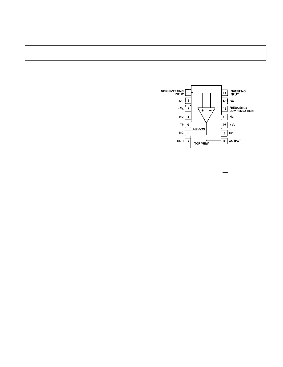
CONNECTION DIAGRAM
Plastic DIP (N) Package
or Cerdip (Q) Package
PRODUCT HIGHLIGHTS
1. All guaranteed dc specifications are 100% tested.
2. The AD5539 drives 50
and 75
loads directly.
3. Input voltage noise is less than 4 nV
Hz
.
4. Low cost RF and video speed performance.
5.
±
2 volt output range into a 150
load.
6. Low cost.
7. Chips available.
PRODUCT DESCRIPTION
The AD5539 is an ultrahigh frequency operational amplifier de-
signed specifically for use in video circuits and RF amplifiers.
Requiring no external compensation for gains greater than 5, it
may be operated at lower gains with the addition of external
compensation.
As a superior replacement for the Signetics NE/SE5539, each
AD5539 is 100% dc tested to meet all of its guaranteed dc
specifications over the full temperature range of the device.
The high slew rate and wide bandwidth of the AD5539 provide
low cost solutions to many otherwise complex and expensive
high frequency circuit design problems.
The AD5539 is available specified to operate over either the
commercial (AD5539JN/JQ) or military (AD5539SQ) tempera-
ture range. The commercial grade is available either in 14-pin
plastic or cerdip packages. The military version is supplied in
the cerdip package. Chip versions are also available.

REV. B
2
AD5539SPECIFICATIONS
(@ +25 C and V
S
= 8 V dc, unless otherwise noted)
AD5539J
AD5539S
Parameter
Min
Typ
Max
Min
Typ
Max
Units
INPUT OFFSET VOLTAGE
Initial Offset
1
2
5
2
3
mV
T
MIN
to T
MAX
6
5
mV
INPUT OFFSET CURRENT
Initial Offset
2
0.1
2
0.1
1
µ
A
T
MIN
to T
MAX
5
3
µ
A
INPUT BIAS CURRENT
Initial
2
V
CM
= 0
6
20
6
13
µ
A
Either Input
T
MIN
to T
MAX
40
25
µ
A
FREQUENCY RESPONSE
R
L
= 150
3
Small Signal Bandwidth
220
220
MHz
A
CL
= 2
4
Gain Bandwidth Product
1400
1400
MHz
A
CL
= 26 dB
Full Power Response
A
CL
= 2
4
68
68
MHz
A
CL
= 7
82
82
MHz
A
CL
= 20
65
65
MHz
Settling Time (1%)
12
12
ns
Slew Rate
600
600
V/
µ
s
Large Signal Propagation Delay
4
4
ns
Total Harmonic Distortion
R
L
=
0.010
0.010
%
R
L
= 100
3
0.016
0.016
%
V
OUT
= 2 V pp
A
CL
= 7, f = 1 kHz
INPUT IMPEDANCE
100
100
k
OUTPUT IMPEDANCE (f <10 MHz)
2
2
INPUT VOLTAGE RANGE
Differential
5
(Max Nondestructive)
250
250
mV
Common-Mode Voltage
(Max Nondestructive)
2.5
2.5
V
Common-Mode Rejection Ratio
V
CM
= 1.7 V
R
S
= 100
70
85
70
85
dB
T
MIN
to T
MAX
60
60
dB
INPUT VOLTAGE NOISE
Wideband RMS Noise (RTI)
5
5
FV
BW = 5 MHz; R
S
= 50
Spot Noise
4
4
nV
Hz
F = 1 kHz; R
S
= 50
OPEN-LOOP GAIN
V
O
= +2.3 V, 1.7 V
R
L
= 150
3
47
52
58
47
52
58
dB
R
L
= 2 k
47
58
48
57
dB
T
MIN
to T
MAX
R
L
= 2 k
43
63
46
60
dB

AD5539J
AD5539S
Parameter
Min
Typ
Max
Min
Typ
Max
Units
OUTPUT CHARACTERISTICS
Positive Output Swing
R
L
= 150
3
+2.3
+2.8
+2.3
+2.8
V
R
L
= 2 k
+2.3
+3.3
+2.5
+3.3
V
T
MIN
to T
MAX
with
R
L
= 2 k
+2.3
+2.3
V
Negative Output Swing
R
L
= 150
3
2.2
1.7
2.2
1.7
V
R
L
= 2 k
2.9
1.7
2.9
2.0
V
T
MIN
to T
MAX
with
R
L
= 2 k
1.5
1.5
V
POWER SUPPLY (No Load, No Resistor to V
S
)
Rated Performance
±
8
±
8
V
Operating Range
4.5
10
4.5
10
V
Quiescent Current
Initial I
CC
+
14
18
14
17
mA
T
MIN
to T
MAX
20
18
mA
Initial I
CC
11
15
11
14
mA
T
MIN
to T
MAX
17
15
mA
PSRR
Initial
100
1000
100
1000
µ
V/V
T
MIN
to T
MAX
2000
2000
µ
V/V
TEMPERATURE RANGE
Operating,
Rated Performance
Commercial (0
°
C to +70
°
C)
AD5539JN, AD5539JQ
Military (55
°
C to +125
°
C)
AD5539SQ
PACKAGE OPTIONS
Plastic (N-14)
AD5539JN
Cerdip (Q-14)
AD5539JQ
AD5539SQ, AD5539SQ/883B
J and S Grade Chips Available
NOTES
1
Input Offset Voltage specifications are guaranteed after 5 minutes of operation at T
A
= +25
°
C.
2
Bias Current specifications are guaranteed maximum at either input after 5 minutes of operation at T
A
= +25
°
C.
3
R
X
= 470
to V
S
.
4
Externally compensated.
5
Defined as voltage between inputs, such that neither exceeds +2.5 V, 5.0 V from ground.
Specifications subject to change without notice.
Specifications in boldface are tested on all production units at final electrical test. Results from those tests are used to calculate outgoing
quality levels. All min and max specifications are guaranteed, although only those shown in boldface are tested on all production units.
REV. B
3
AD5539
AD5539
REV. B
4
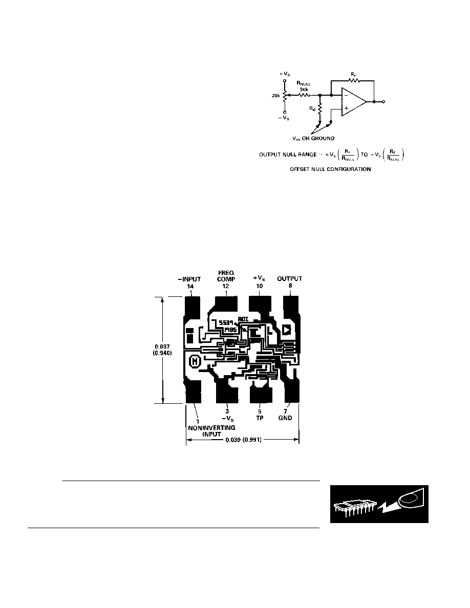
OFFSET NULL CONFlGURATION
METALIZATION PHOTOGRAPH
Dimensions shown in inches and (mm).
Contact factory for latest dimensions.
ABSOLUTE MAXIMUM RATINGS
*
Supply Voltage . . . . . . . . . . . . . . . . . . . . . . . . . . . . . . . .
±
10 V
Internal Power Dissipation . . . . . . . . . . . . . . . . . . . . . 550 mW
Input Voltage . . . . . . . . . . . . . . . . . . . . . . . . . . +2.5 V, 5.0 V
Differential Input Voltage . . . . . . . . . . . . . . . . . . . . . . 0.25 V
Storage Temperature Range (Q) . . . . . . . . . 65
°
C to +150
°
C
Storage Temperature Range (N) . . . . . . . . . 65
°
C to +125
°
C
Operating Temperature Range
AD5539JN . . . . . . . . . . . . . . . . . . . . . . . . . . . 0
°
C to +70
°
C
AD5539JQ . . . . . . . . . . . . . . . . . . . . . . . . . . . 0
°
C to +70
°
C
AD5539SQ . . . . . . . . . . . . . . . . . . . . . . . 55
°
C to +125
°
C
Lead Temperature Range (Soldering 60 Seconds) . . . +300
°
C
*
Stresses above those listed under "Absolute Maximum Ratings" may cause
permanent damage to the device. This is a stress rating only and functional
operation of the device at these or any other conditions above those indicated in
the operational section of this specification is not implied. Exposure to absolute
maximum rating conditions for extended periods may affect device reliability.
WARNING!
ESD SENSITIVE DEVICE
CAUTION
ESD (electrostatic discharge) sensitive device. Electrostatic charges as high as 4000 V readily
accumulate on the human body and test equipment and can discharge without detection.
Although the AD5539 features proprietary ESD protection circuitry, permanent damage may
occur on devices subjected to high energy electrostatic discharges. Therefore, proper ESD
precautions are recommended to avoid performance degradation or loss of functionality.
REV. B
5
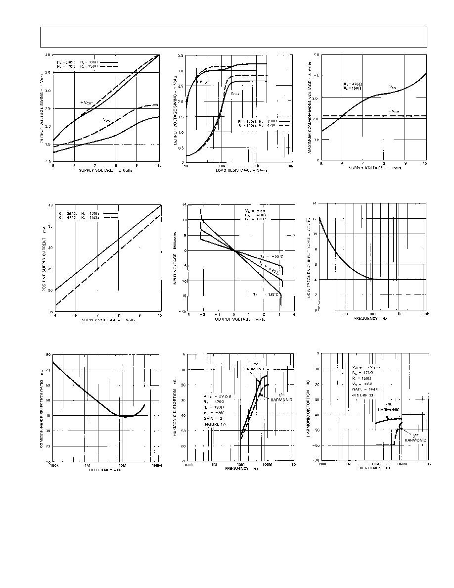
Figure 1. Output Voltage Swing
vs. Supply Voltage
Figure 4. Positive Supply Current
vs. Supply Voltage
Figure 7. Common-Mode
Rejection Ratio vs. Frequency
Figure 2. Output Voltage Swing
vs. Load Resistance
Figure 5. Input Voltage vs. Output
Voltage for Various Temperatures
Figure 8. Harmonic Distortion
vs. Frequency Low Gain
Figure 3. Maximum Common-
Mode Voltage vs. Supply Voltage
Figure 6. Low Frequency Input
Noise vs. Frequency
Figure 9. Harmonic Distortion
vs. Frequency High Gain
Typical Characteristics
--
AD5539