 | –≠–ª–µ–∫—Ç—Ä–æ–Ω–Ω—ã–π –∫–æ–º–ø–æ–Ω–µ–Ω—Ç: AD574ALD | –°–∫–∞—á–∞—Ç—å:  PDF PDF  ZIP ZIP |
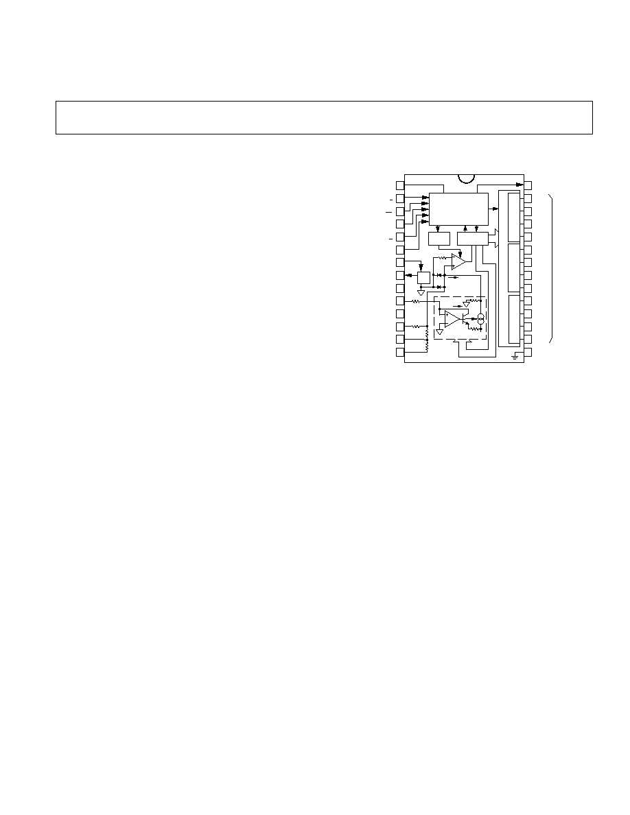
BLOCK DIAGRAM AND
PIN CONFIGURATION
1
14
28
15
2
3
4
5
6
7
8
9
10
11
12
13
27
26
25
24
23
22
21
20
19
18
17
16
CONTROL
CLOCK
SAR
3
S
T
A
T
E
O
U
T
P
U
T
B
U
F
F
E
R
S
MSB
N
I
B
B
L
E
N
I
B
B
L
E
N
I
B
B
L
E
LSB
10V
REF
12
12
C
B
A
12
AD574A
3k
19.95k
9.95k
5k
5k
N
DAC
V
EE
8k
I
REF
COMP
DIGITAL COMMON
DC
I
DAC
I
DAC
=
4 x N x I
REF
+5V SUPPLY
V
LOGIC
DATA MODE SELECT
12/8
STATUS
STS
DB11
MSB
DB10
DB9
DB8
DB7
DB6
DB5
DB4
DB3
DB2
DB1
DB0
LSB
DIGITAL
DATA
OUTPUTS
CHIP SELECT
CS
BYTE ADDRESS/
SHORT CYCLE
A
O
READ/CONVERT
R/C
CHIP ENABLE
CE
+12/+15V SUPPLY
V
CC
+10V REFERENCE
REF OUT
ANALOG COMMON
AC
REFERENCE INPUT
REF IN
-12/-15V SUPPLY
V
EE
BIPOLAR OFFSET
BIP OFF
10V SPAN INPUT
10V
IN
20V SPAN INPUT
20V
IN
REV. B
Information furnished by Analog Devices is believed to be accurate and
reliable. However, no responsibility is assumed by Analog Devices for its
use, nor for any infringements of patents or other rights of third parties
which may result from its use. No license is granted by implication or
otherwise under any patent or patent rights of Analog Devices.
a
Complete
12-Bit A/D Converter
AD574A*
One Technology Way, P.O. Box 9106, Norwood, MA 02062-9106, U.S.A.
Tel: 617/329-4700
Fax: 617/326-8703
PRODUCT DESCRIPTION
The AD574A is a complete 12-bit successive-approximation
analog-to-digital converter with 3-state output buffer circuitry
for direct interface to an 8- or 16-bit microprocessor bus. A high
precision voltage reference and clock are included on-chip, and
the circuit guarantees full-rated performance without external
circuitry or clock signals.
The AD574A design is implemented using Analog Devices'
Bipolar/I
2
L process, and integrates all analog and digital func-
tions on one chip. Offset, linearity and scaling errors are mini-
mized by active laser-trimming of thin-film resistors at the wafer
stage. The voltage reference uses an implanted buried Zener for
low noise and low drift. On the digital side, I
2
L logic is used for
the successive-approximation register, control circuitry and
3-state output buffers.
The AD574A is available in six different grades. The AD574AJ,
K, and L grades are specified for operation over the 0
∞
C to
+70
∞
C temperature range. The AD574AS, T, and U are speci-
fied for the ≠55
∞
C to +125
∞
C range. All grades are available in a
28-pin hermetically-sealed ceramic DIP. Also, the J, K, and L
grades are available in a 28-pin plastic DIP and PLCC, and the
J and K grades are available in ceramic LCC.
The S, T, and U grades in ceramic DIP or LCC are available
with optional processing to MIL-STD-883C Class B; the T
and U grades are available as JAN QPL. The Analog Devices'
Military Products Databook should be consulted for details on
/883B testing of the AD574A.
*Protected by U.S. Patent Nos. 3,803,590; 4,213,806; 4,511,413; RE 28,633 .
FEATURES
Complete 12-Bit A/D Converter with Reference
and Clock
8- and 16-Bit Microprocessor Bus Interface
Guaranteed Linearity Over Temperature
0 C to +70 C ≠ AD574AJ, K, L
≠55 C to +125 C ≠ AD574AS, T, U
No Missing Codes Over Temperature
35 s Maximum Conversion Time
Buried Zener Reference for Long-Term Stability
and Low Gain T.C. 10 ppm/ C max AD574AL
12.5 ppm/ C max AD574AU
Ceramic DIP, Plastic DIP or PLCC Package
Available in Higher Speed, Pinout-Compatible Versions
(15 s AD674B, 80 s AD774B; 10 s (with SHA) AD1674)
Available in Versions Compliant with MIL-STD-883 and
JAN QPL
PRODUCT HIGHLIGHTS
1. The AD574A interfaces to most 8- or 16-bit microproces-
sors. Multiple-mode three-state output buffers connect di-
rectly to the data bus while the read and convert commands
are taken from the control bus. The 12 bits of output data
can be read either as one 12-bit word or as two 8-bit bytes
(one with 8 data bits, the other with 4 data bits and 4 trailing
zeros).
2. The precision, laser-trimmed scaling and bipolar offset resis-
tors provide four calibrated ranges: 0 volts to +10 volts and 0
volts to +20 volts unipolar, ≠5 volts to +5 volts and ≠10 volts
to +10 volts bipolar. Typical bipolar offset and full-scale cali-
bration errors of
±
0.1% can be trimmed to zero with one ex-
ternal component each.
3. The internal buried Zener reference is trimmed to 10.00
volts with 0.2% maximum error and 15 ppm/
∞
C typical T.C.
The reference is available externally and can drive up to
1.5 mA beyond the requirements of the reference and bipolar
offset resistors.
4. AD674B (15
µ
s) and AD774B (8
µ
s) provide higher speed,
pin compatibility; AD1674 (10
µ
s) includes on-chip Sample-
Hold Amplifier (SHA).
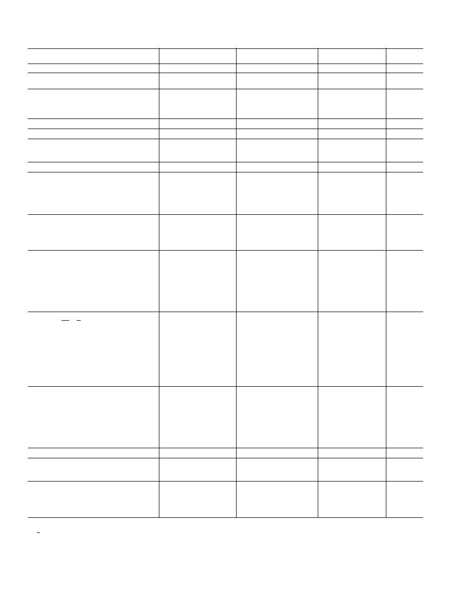
AD574A≠SPECIFICATIONS
AD574AJ
AD574AK
AD574AL
Model
Min
Typ
Max
Min
Typ
Max
Min
Typ
Max
Units
RESOLUTION
12
12
12
Bits
LINEARITY ERROR @ +25
∞
C
±
1
±
1/2
±
1/2
LSB
T
MIN
to T
MAX
±
1
±
1/2
±
1/2
LSB
DIFFERENTIAL LINEARITY ERROR
(Minimum Resolution for Which No
Missing Codes are Guaranteed)
T
MIN
to T
MAX
11
12
12
Bits
UNIPOLAR OFFSET (Adjustable to Zero)
±
2
±
1
±
1
LSB
BIPOLAR OFFSET (Adjustable to Zero)
±
4
±
4
±
2
LSB
FULL-SCALE CALIBRATION ERROR
(With Fixed 50
Resistor from REF OUT to REF IN)
(Adjustable to Zero)
0.25
0.25
0.125
% of FS
TEMPERATURE RANGE
0
+70
0
+70
0
+70
∞
C
TEMPERATURE COEFFICIENTS
(Using Internal Reference)
T
MIN
to T
MAX
Unipolar Offset
±
2 (10)
±
1 (5)
±
1 (5)
LSB (ppm/
∞
C)
Bipolar Offset
±
2 (10)
±
1 (5)
±
1 (5)
LSB (ppm/
∞
C)
Full-Scale Calibration
±
9 (50)
±
5 (27)
±
2 (10) LSB (ppm/
∞
C)
POWER SUPPLY REJECTION
Max Change in Full-Scale Calibration
V
CC
= 15 V
±
1.5 V or 12 V
±
0.6 V
±
2
±
1
±
1
LSB
V
LOGIC
= 5 V
±
0.5 V
±
1/2
±
1/2
±
1/2
LSB
V
EE
= ≠15 V
±
1.5 V or ≠12 V
±
0.6 V
±
2
±
1
±
1
LSB
ANALOG INPUT
Input Ranges
Bipolar
≠5
+5
≠5
+5
≠5
+5
Volts
≠10
+10
≠10
+10
≠10
+10
Volts
Unipolar
0
+10
0
+10
0
+10
Volts
0
+20
0
+20
0
+20
Volts
Input Impedance
10 Volt Span
3
5
7
3
5
7
3
5
7
k
20 Volt Span
6
10
14
6
10
14
6
10
14
k
DIGITAL CHARACTERISTICS
1
(T
MIN
≠T
MAX
)
Inputs
2
(CE, CS, R/C, A
0
)
Logic "1" Voltage
+2.0
+5.5
+2.0
+5.5
+2.0
+5.5
Volts
Logic "0" Voltage
≠0.5
+0.8
≠0.5
+0.8
≠0.5
+0.8
Volts
Current
≠20
+20
≠20
+20
≠20
+20
µ
A
Capacitance
5
5
5
pF
Output (DB11≠DB0, STS)
Logic "1" Voltage (I
SOURCE
500
µ
A)
+2.4
+2.4
+2.4
Volts
Logic "0" Voltage (I
SINK
1.6 mA)
+0.4
+0.4
+0.4
Volts
Leakage (DB11≠DB0, High-Z State)
≠20
+20
≠20
+20
≠20
+20
µ
A
Capacitance
5
5
5
pF
POWER SUPPLIES
Operating Range
V
LOGIC
+4.5
+5.5
+4.5
+5.5
+4.5
+5.5
Volts
V
CC
+11.4
+16.5
+11.4
+16.5
+11.4
+16.5
Volts
V
EE
≠11.4
≠16.5
≠11.4
≠16.5
≠11.4
≠16.5
Volts
Operating Current
I
LOGIC
30
40
30
40
30
40
mA
I
CC
2
5
2
5
2
5
mA
I
EE
18
30
18
30
18
30
mA
POWER DISSIPATION
390
725
390
725
390
725
mW
INTERNAL REFERENCE VOLTAGE
9.98
10.0
10.02
9.98
10.0
10.02
9.99
10.0
10.01
Volts
Output Current (Available for External Loads)
3
1.5
1.5
1.5
mA
(External Load Should not Change During Conversion)
PACKAGE OPTIONS
4
Ceramic (D-28)
AD574ASD
AD574AKD
AD574ALD
Plastic (N-28)
AD574AJN
AD574AKN
AD574ALN
PLCC (P-28A)
AD574AJP
AD574AKP
LCC (E-28A)
AD574AJE
AD574AKE
NOTES
1
Detailed Timing Specifications appear in the Timing Section.
2
12/8 Input is not TTL-compatible and must be hard wired to V
LOGIC
or Digital Common.
3
The reference should be buffered for operation on
±
12 V supplies.
4
D = Ceramic DIP; N = Plastic DIP; P = Plastic Leaded Chip Carrier.
Specifications subject to change without notice.
(@ +25 C with V
CC
= +15 V or +12 V, V
LOGIC
= +5 V, V
EE
= ≠15 V or ≠12 V
unless otherwise noted)
REV. B
≠2≠

AD574AS
AD574AT
AD574AU
Model
Min
Typ
Max
Min
Typ
Max
Min
Typ
Max
Units
RESOLUTION
12
12
12
Bits
LINEARITY ERROR @ +25
∞
C
±
1
±
1/2
±
1/2
LSB
T
MIN
to T
MAX
±
1
±
1
±
1
LSB
DIFFERENTIAL LINEARITY ERROR
(Minimum Resolution for Which No
Missing Codes are Guaranteed)
T
MIN
to T
MAX
11
12
12
Bits
UNIPOLAR OFFSET (Adjustable to Zero)
±
2
±
1
±
1
LSB
BIPOLAR OFFSET (Adjustable to Zero)
±
4
±
4
±
2
LSB
FULL-SCALE CALIBRATION ERROR
(With Fixed 50
Resistor from REF OUT to REF IN)
(Adjustable to Zero)
0.25
0.25
0.125
% of FS
TEMPERATURE RANGE
≠55
+125
≠55
+125
≠55
+125
∞
C
TEMPERATURE COEFFICIENTS
(Using Internal Reference)
(T
MIN
to T
MAX
)
Unipolar Offset
±
2 (5)
±
1 (2.5)
±
1 (2.5)
LSB (ppm/
∞
C)
Bipolar Offset
±
4 (10)
±
2 (5)
±
1 (2.5)
LSB (ppm/
∞
C)
Full-Scale Calibration
±
20 (50)
±
10 (25)
±
5 (12.5) LSB (ppm/
∞
C)
POWER SUPPLY REJECTION
Max Change in Full-Scale Calibration
V
CC
= 15 V
±
1.5 V or 12 V
±
0.6 V
±
2
±
1
±
1
LSB
V
LOGIC
= 5 V
±
0.5 V
±
1/2
±
1/2
±
1/2
LSB
V
EE
= ≠15 V
±
1.5 V or ≠12 V
±
0.6 V
±
2
±
1
±
1
LSB
ANALOG INPUT
Input Ranges
Bipolar
≠5
+5
≠5
+5
≠5
+5
Volts
≠10
+10
≠10
+10
≠10
+10
Volts
Unipolar
0
+10
0
+10
0
+10
Volts
0
+20
0
+20
0
+20
Volts
Input Impedance
10 Volt Span
3
5
7
3
5
7
3
5
7
k
20 Volt Span
6
10
14
6
10
14
6
10
14
k
DIGITAL CHARACTERISTICS
1
(T
MIN
≠T
MAX
)
Inputs
2
(CE, CS, R/C, A
0
)
Logic "1" Voltage
+2.0
+5.5
+2.0
+5.5
+2.0
+5.5
Volts
Logic "0" Voltage
≠0.5
+0.8
≠0.5
+0.8
≠0.5
+0.8
Volts
Current
≠20
+20
≠20
+20
≠20
+20
µ
A
Capacitance
5
5
5
pF
Output (DB11≠DB0, STS)
Logic "1" Voltage (I
SOURCE
500
µ
A)
+2.4
+2.4
+2.4
Volts
Logic "0" Voltage (I
SINK
1.6 mA)
+0.4
+0.4
+0.4
Volts
Leakage (DB11≠DB0, High-Z State)
≠20
+20
≠20
+20
≠20
+20
µ
A
Capacitance
5
5
5
pF
POWER SUPPLIES
Operating Range
V
LOGIC
+4.5
+5.5
+4.5
+5.5
+4.5
+5.5
Volts
V
CC
+11.4
+16.5
+11.4
+16.5
+11.4
+16.5
Volts
V
EE
≠11.4
≠16.5
≠11.4
≠16.5
≠11.4
≠16.5
Volts
Operating Current
I
LOGIC
30
40
30
40
30
40
mA
I
CC
2
5
2
5
2
5
mA
I
EE
18
30
18
30
18
30
mA
POWER DISSIPATION
390
725
390
725
390
725
mW
INTERNAL REFERENCE VOLTAGE
9.98
10.0
10.02
9.98
10.0
10.02
9.99
10.0
10.01
Volts
Output Current (Available for External Loads)
3
1.5
1.5
1.5
mA
(External Load Should not Change During Conversion)
PACKAGE OPTION
4
Ceramic (D-28)
AD574ASD
AD574ATD
AD574AUD
NOTES
1
Detailed Timing Specifications appear in the Timing Section.
2
12/8 Input is not TTL-compatible and must be hard wired to V
LOGIC
or Digital Common.
3
The reference should be buffered for operation on
±
12 V supplies.
4
D = Ceramic DIP.
Specifications subject to change without notice.
AD574A
REV. B
≠3≠
AD574A
REV. B
≠4≠
ORDERING GUIDE
Resolution
Max
Temperature
Linearity Error
No Missing Codes
Full Scale
Model
1
Range
Max (T
MIN
to T
MAX
)
(T
MIN
to T
MAX
)
T.C. (ppm/
∞
C)
AD574AJ(X)
0
∞
C to +70
∞
C
±
1 LSB
11 Bits
50.0
AD574AK(X)
0
∞
C to +70
∞
C
±
1/2 LSB
12 Bits
27.0
AD574AL(X)
0
∞
C to +70
∞
C
±
1/2 LSB
12 Bits
10.0
AD574AS(X)
2
≠55
∞
C to +125
∞
C
±
1 LSB
11 Bits
50.0
AD574AT(X)
2
≠55
∞
C to +125
∞
C
±
1 LSB
12 Bits
25.0
AD574AU(X)
2
≠55
∞
C to +125
∞
C
±
1 LSB
12 Bits
12.5
NOTES
1
X = Package designator. Available packages are: D (D-28) for all grades. E (E-28A) for J and K grades and /883B processed S, T
and U grades. N (N-28) for J, K, and L grades. P (P-28A) for PLCC in J, K grades. Example: AD574AKN is K grade in plastic DIP.
2
For details on grade and package offerings screened in accordance with MIL-STD-883, refer to Analog Devices Military Products
Databook.
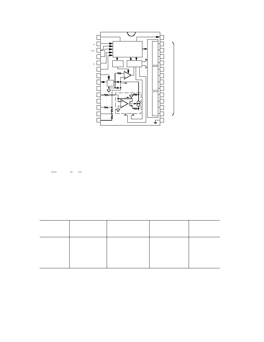
1
14
28
15
2
3
4
5
6
7
8
9
10
11
12
13
27
26
25
24
23
22
21
20
19
18
17
16
CONTROL
CLOCK
SAR
3
S
T
A
T
E
O
U
T
P
U
T
B
U
F
F
E
R
S
MSB
N
I
B
B
L
E
N
I
B
B
L
E
N
I
B
B
L
E
LSB
10V
REF
12
12
C
B
A
12
AD574A
3k
19.95k
9.95k
5k
5k
N
DAC
V
EE
8k
I
REF
COMP
DIGITAL COMMON
DC
I
DAC
I
DAC
=
4 x N x I
REF
+5V SUPPLY
V
LOGIC
DATA MODE SELECT
12/8
STATUS
STS
DB11
MSB
DB10
DB9
DB8
DB7
DB6
DB5
DB4
DB3
DB2
DB1
DB0
LSB
DIGITAL
DATA
OUTPUTS
CHIP SELECT
CS
BYTE ADDRESS/
SHORT CYCLE
A
O
READ/CONVERT
R/C
CHIP ENABLE
CE
+12/+15V SUPPLY
V
CC
+10V REFERENCE
REF OUT
ANALOG COMMON
AC
REFERENCE INPUT
REF IN
-12/-15V SUPPLY
V
EE
BIPOLAR OFFSET
BIP OFF
10V SPAN INPUT
10V
IN
20V SPAN INPUT
20V
IN
AD574A Block Diagram and Pin Configuration
ABSOLUTE MAXIMUM RATINGS*
(Specifications apply to all grades, except where noted)
V
CC
to Digital Common . . . . . . . . . . . . . . . . . . 0 V to +16.5 V
V
EE
to Digital Common . . . . . . . . . . . . . . . . . . . 0 V to ≠16.5 V
V
LOGIC
to Digital Common . . . . . . . . . . . . . . . . . . 0 V to +7 V
Analog Common to Digital Common . . . . . . . . . . . . . . .
±
1 V
Control Inputs (CE, CS, A
O
12/8, R/C) to
Digital Common . . . . . . . . . . . . . . ≠0.5 V to V
LOGIC
+ 0.5 V
Analog Inputs (REF IN, BIP OFF, 10 V
IN
) to
Analog Common . . . . . . . . . . . . . . . . . . . . . . . . . V
EE
to V
CC
20 V
IN
to Analog Common . . . . . . . . . . . . . . . . . . . . . .
±
24 V
REF OUT . . . . . . . . . . . . . . . . . . Indefinite Short to Common
Momentary Short to V
CC
Chip Temperature . . . . . . . . . . . . . . . . . . . . . . . . . . . . . 175
∞
C
Power Dissipation . . . . . . . . . . . . . . . . . . . . . . . . . . . . 825 mW
Lead Temperature (Soldering, 10 sec). . . . . . . . . . . . . +300
∞
C
Storage Temperature (Ceramic) . . . . . . . . . . ≠65
∞
C to +150
∞
C
(Plastic) . . . . . . . . . . . . . . . . . . . . . . . . . . . ≠25
∞
C to +100
∞
C
*Stresses above those listed under "Absolute Maximum Ratings" may cause
permanent damage to the device. This is a stress rating only and functional
operation of the device at these or any other conditions above those indicated in the
operational sections of this specification is not implied. Exposure to absolute
maximum rating conditions for extended periods may affect device reliability.

AD574A
REV. B
≠5≠
DEFINITIONS OF SPECIFICATIONS
LINEARITY ERROR
Linearity error refers to the deviation of each individual code
from a line drawn from "zero" through "full scale". The point
used as "zero" occurs 1/2 LSB (1.22 mV for 10 volt span) be-
fore the first code transition (all zeros to only the LSB "on").
"Full scale" is defined as a level 1 1/2 LSB beyond the last code
transition (to all ones). The deviation of a code from the true
straight line is measured from the middle of each particular
code.
The AD574AK, L, T, and U grades are guaranteed for maxi-
mum nonlinearity of
±
1/2 LSB. For these grades, this means
that an analog value which falls exactly in the center of a given
code width will result in the correct digital output code. Values
nearer the upper or lower transition of the code width may pro-
duce the next upper or lower digital output code. The AD574AJ
and S grades are guaranteed to
±
1 LSB max error. For these
grades, an analog value which falls within a given code width
will result in either the correct code for that region or either
adjacent one.
Note that the linearity error is not user-adjustable.
DIFFERENTIAL LINEARITY ERROR (NO MISSING
CODES)
A specification which guarantees no missing codes requires that
every code combination appear in a monotonic increasing se-
quence as the analog input level is increased. Thus every code
must have a finite width. For the AD574AK, L, T, and U
grades, which guarantee no missing codes to 12-bit resolution,
all 4096 codes must be present over the entire operating tem-
perature ranges. The AD574AJ and S grades guarantee no miss-
ing codes to 11-bit resolution over temperature; this means that
all code combinations of the upper 11 bits must be present; in
practice very few of the 12-bit codes are missing.
UNIPOLAR OFFSET
The first transition should occur at a level 1/2 LSB above analog
common. Unipolar offset is defined as the deviation of the actual
transition from that point. This offset can be adjusted as discussed
on the following two pages. The unipolar offset temperature
coefficient specifies the maximum change of the transition point
over temperature, with or without external adjustment.
BIPOLAR OFFSET
In the bipolar mode the major carry transition (0111 1111 1111
to 1000 0000 0000) should occur for an analog value 1/2 LSB
below analog common. The bipolar offset error and temperature
coefficient specify the initial deviation and maximum change in
the error over temperature.
QUANTIZATION UNCERTAINTY
Analog-to-digital converters exhibit an inherent quantization
uncertainty of
±
1/2 LSB. This uncertainty is a fundamental
characteristic of the quantization process and cannot be reduced
for a converter of given resolution.
LEFT-JUSTIFIED DATA
The data format used in the AD574A is left-justified. This
means that the data represents the analog input as a fraction of
full-scale, ranging from 0 to
4095
4096
. This implies a binary point
to the left of the MSB.
FULL-SCALE CALIBRATION ERROR
The last transition (from 1111 1111 1110 to 1111 1111 1111)
should occur for an analog value 1 1/2 LSB below the nominal
full scale (9.9963 volts for 10.000 volts full scale). The full-scale
calibration error is the deviation of the actual level at the last
transition from the ideal level. This error, which is typically
0.05% to 0.1% of full scale, can be trimmed out as shown in
Figures 3 and 4.
TEMPERATURE COEFFICIENTS
The temperature coefficients for full-scale calibration, unipolar
offset, and bipolar offset specify the maximum change from the
initial (25
∞
C) value to the value at T
MIN
or T
MAX
.
POWER SUPPLY REJECTION
The standard specifications for the AD574A assume use of
+5.00 V and
±
15.00 V or
±
12.00 V supplies. The only effect of
power supply error on the performance of the device will be a
small change in the full-scale calibration. This will result in a
linear change in all lower order codes. The specifications show
the maximum full-scale change from the initial value with the
supplies at the various limits.
CODE WIDTH
A fundamental quantity for A/D converter specifications is the
code width. This is defined as the range of analog input values
for which a given digital output code will occur. The nominal
value of a code width is equivalent to 1 least significant bit
(LSB) of the full-scale range or 2.44 mV out of 10 volts for a
12-bit ADC.
THE AD574A OFFERS GUARANTEED MAXIMUM LINEARITY ERROR OVER THE FULL OPERATING
TEMPERATURE RANGE