 | –≠–ª–µ–∫—Ç—Ä–æ–Ω–Ω—ã–π –∫–æ–º–ø–æ–Ω–µ–Ω—Ç: AD664 | –°–∫–∞—á–∞—Ç—å:  PDF PDF  ZIP ZIP |
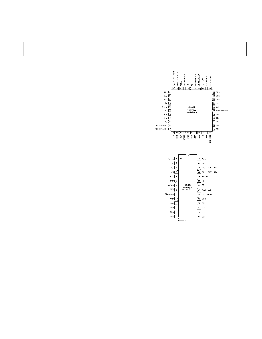
PIN CONFIGURATIONS
44-Pin Package
28-Pin DIP Package
REV. C
Information furnished by Analog Devices is believed to be accurate and
reliable. However, no responsibility is assumed by Analog Devices for its
use, nor for any infringements of patents or other rights of third parties
which may result from its use. No license is granted by implication or
otherwise under any patent or patent rights of Analog Devices.
a
Monolithic
12-Bit Quad DAC
AD664
FEATURES
Four Complete Voltage Output DACs
Data Register Readback Feature
"Reset to Zero" Override
Multiplying Operation
Double-Buffered Latches
Surface Mount and DIP Packages
MIL-STD-883 Compliant Versions Available
APPLICATIONS
Automatic Test Equipment
Robotics
Process Control
Disk Drives
Instrumentation
Avionics
One Technology Way, P.O. Box 9106, Norwood, MA 02062-9106, U.S.A.
Tel: 617/329-4700
Fax: 617/326-8703
PRODUCT DESCRIPTION
The AD664 is four complete 12-bit, voltage-output DACs on
one monolithic IC chip. Each DAC has a double-buffered input
latch structure and a data readback function. All DAC read and
write operations occur through a single microprocessor-compatible
I/O port.
The I/O port accommodates 4-, 8- or 12-bit parallel words al-
lowing simple interfacing with a wide variety of microprocessors.
A reset to zero control pin is provided to allow a user to simulta-
neously reset all DAC outputs to zero, regardless of the contents
of the input latch. Any one or all of the DACs may be placed in
a transparent mode allowing immediate response by the outputs
to the input data.
The analog portion of the AD664 consists of four DAC cells,
four output amplifiers, a control amplifier and switches. Each
DAC cell is an inverting R-2R type. The output current from
each DAC is switched to the on-board application resistors and
output amplifier. The output range of each DAC cell is pro-
grammed through the digital I/O port and may be set to unipo-
lar or bipolar range, with a gain of one or two times the reference
voltage. All DACs are operated from a single external reference.
The functional completeness of the AD664 results from the
combination of Analog Devices' BiMOS II process, laser-trimmed
thin-film resistors and double-level metal interconnects.
PRODUCT HIGHLIGHTS
1. The AD664 provides four voltage-output DACs on one chip
offering the highest density 12-bit D/A function available.
2. The output range of each DAC is fully and independently
programmable.
3. Readback capability allows verification of contents of the in-
ternal data registers.
4. The asynchronous RESET control returns all D/A outputs
to zero volts.
5. DAC-to-DAC matching performance is specified and tested.
6. Linearity error is specified to be 1/2 LSB at room tempera-
ture and 3/4 LSB maximum for the K, B and T grades.
7. DAC performance is guaranteed to be monotonic over the
full operating temperature range.
8. Readback buffers have tristate outputs.
9. Multiplying-mode operation allows use with fixed or vari-
able, positive or negative external references.
10. The AD664 is available in versions compliant with MIL-
STD-883. Refer to the Analog Devices Military Products
Databook or current AD664/883B data sheet for detailed
specifications.

AD664≠SPECIFICATIONS
(V
LL
= +5 V, V
CC
= +15 V, V
EE
= ≠15 V, V
REF
= +10 V, T
A
= +25 C
unless otherwise noted)
REV. C
≠2≠
Model
JN/JP/AD/AJ/SD
KN/KP/BD/BJ/BE/TD/TE
Min
Typ
Max
Min
Typ
Max
Units
RESOLUTION
12
12
*
*
Bits
ANALOG OUTPUT
Voltage Range
1
UNI Versions
0
V
CC
≠ 2.0
2
*
*
Volts
BIP Versions
V
EE
+ 2.0
2
V
CC
≠ 2.0
2
*
*
Volts
Output Current
5
*
mA
Load Resistance
2
*
k
Load Capacitance
500
*
pF
Short-Circuit Current
25
40
*
*
mA
ACCURACY
Gain Error
≠7
±
3
7
≠5
±
2
5
LSB
Unipolar Offset
≠2
±
1/2
2
≠1
±
1/4
1
LSB
Bipolar Zero
3
≠3
±
3/4
3
≠2
±
1/2
2
LSB
Linearity Error
4
≠3/4
±
1/2
3/4
≠1/2
±
1/4
1/2
LSB
Linearity T
MIN
to T
MAX
≠1
±
3/4
1
≠3/4
±
1/2
3/4
LSB
Differential Linearity
≠3/4
3/4
≠1/2
1/2
LSB
Differential Linearity T
MIN
to T
MAX
Monotonic @ All Temperatures
Monotonic @ All Temperatures
Gain Error Drift
Unipolar 0 V to +10 V Mode
≠12
±
7
12
≠10
±
5
10
ppm of FSR
5
/
∞
C
Bipolar ≠5 V to +5 V Mode
≠12
±
7
12
≠10
±
5
10
ppm of FSR/
∞
C
Bipolar ≠10 V to +10 V Mode
≠12
±
7
12
≠10
±
5
10
ppm of FSR/
∞
C
Unipolar Offset Drift
Unipolar 0 V to +10 V Mode
≠3
±
l.5
3
≠2
±
l
2
ppm of FSR/
∞
C
Bipolar Zero Drift
Bipolar ≠5 V to +5 V Mode
≠12
±
7
12
≠10
±
5
10
ppm of FSR/
∞
C
Bipolar ≠10 V to +10 V Mode
≠12
±
7
12
≠10
±
5
10
ppm of FSR/
∞
C
REFERENCE INPUT
Input Resistance
1.3
2. 6
*
*
k
Voltage Range
6
V
EE
+ 2.0
2
V
CC
≠ 2.0
2
*
*
Volts
POWER REOUIREMENTS
V
LL
4.5
5.0
5.5
*
*
*
Volts
I
LL
@ V
IH
, V
IL
= 5 V, 0 V
0.1
1
*
*
mA
@ V
IH
, V
IL
= 2.4 V, 0.4 V
3
6
*
*
mA
V
CC
/V
EE
11.4
16.5
*
*
Volts
I
CC
12
15
*
*
mA
I
EE
15
19
*
*
mA
Total Power
400
525
*
*
mW
ANALOG GROUND CURRENT
7
≠600
±
400
+600
*
*
*
µ
A
MATCHING PERFORMANCE
Gain
8
≠6
±
3
6
≠4
±
2
4
LSB
Offset
9
≠2
±
1/2
2
≠1
±
1/4
1
LSB
Bipolar Zero
10
≠3
±
1
3
≠2
±
1
2
LSB
Linearity
11
≠1.5
±
1/2
1.5
≠1
±
1/2
1
LSB
CROSSTALK
Analog
≠90
*
dB
Digital
≠60
*
dB
DYNAMIC PERFORMANCE (R
L
= 2 k
, C
L
= 500 pF)
Settling Time to
±
1/2 LSB
Off
Bits
On, GAIN = 1, V
REF
= 10
8
10
*
*
µ
s
Settling Time to
±
1/2 LSB
≠10
V
REF
10 V, GAIN = 1, Bits On
10
*
µ
s
Glitch Impulse
500
*
nV-sec
MULTIPLYING MODE PERFORMANCE
Reference Feedthrough @ 1 kHz
≠75
*
dB
Reference ≠3 dB Bandwidth
70
*
kHz
POWER SUPPLY GAIN SENSITIVITY
11.4 V
V
CC
16.5 V
±
2
5
*
*
ppm/%
≠16.5 V
V
EE
≠11.4 V
±
2
5
*
*
ppm/%
4.5 V
V
LL
5.5 V
±
2
5
*
*
ppm/%

AD664
Model
JN/JP/AD/AJ/SD
KN/KP/BD/BJ/BE/TD/TE
Min
Typ
Max
Min
Typ
Max
Units
DIGITAL INPUTS
V
IH
2.0
*
Volts
V
IL
0
0.8
*
*
Volts
Data Inputs
I
IH
@ V
IN
= V
LL
≠10
±
1
10
*
*
*
µ
A
I
IL
@ V
IN
= DGND
≠10
±
1
10
*
*
*
µ
A
CS
/DS0/DS1/RST/RD/LS
I
IH
@ V
IN
= V
LL
≠10
±
1
10
*
*
*
µ
A
I
IL
@ V
IN
= V
LL
≠10
±
1
10
*
*
*
µ
A
MS
/TR
12
I
IH
@ V
IN
= V
LL
≠10
5
10
*
*
*
µ
A
I
IL
@ V
IN
= DGND
≠10
≠5
0
*
*
*
µ
A
QS0
/QSl/QS2
l2
I
IH
@ V
IN
= V
LL
≠10
5
10
*
*
*
µ
A
I
IL
@ V
IN
= DGND
≠10
±
1
10
*
*
*
µ
A
DIGITAL OUTPUTS
V
OL
@ 1.6 mA Sink
0.4
*
Volts
V
OH
@ 0.5 mA Source
2.4
*
Volts
TEMPERATURE RANGE
JN/JP/KN/KP
0
+70
*
*
∞
C
AD/AJ/BD/BJ/BE
≠ 40
+85
*
*
∞
C
SD/TD/TE
≠55
+125
*
*
∞
C
NOTES
1
A minimum power supply of
±
12.0 V is required for 0 V to +10 V and
±
10 V operation. A minimum power supply of
±
11.4 V is required for ≠5 V to +5 V operation.
2
For V
CC
< +12 V and V
EE
> ≠12 V. Voltage not to exeeed 10 V maximum.
3
Bipolar zero error is the difference from the ideal output (0 volts) and the actual output voltage with code 100 000 000 000 applied to the inputs.
4
Linearity error is defined as the maximum deviation of the actual DAC output from the ideal output (a straight line drawn from 0 to F.S. ≠ 1 LSB).
5
FSR means Full-Scale Range and is 20 V for
±
10 V range and 10 V for
±
5 V range.
6
A minimum power supply of
±
12.0 V is required for a 10 V reference voltage.
7
Analog Ground Current is input code dependent.
8
Gain error matching is the largest difference in gain error between any two DACs in one package.
9
Offset error matching is the largest difference in offset error between any two DACs in one package.
10
Bipolar zero error matching is the largest difference in bipolar zero error between any two DACs in one package.
11
Linearity error matching is the difference in the worst ease linearity error between any two DACs in one package.
12
44-pin versions only.
*Specifications same as JN/JP/AD/AJ/SD.
Specifications subject to change without notice.
Specifications shown in boldface are tested on all production units at final electrical test. Results from those tests are used to calculate outgoing quality levels. All min
and max specifications are guaranteed, although only those shown in boldface are tested on all production units.
ABSOLUTE MAXIMUM RATINGS*
V
LL
to DGND . . . . . . . . . . . . . . . . . . . . . . . . . . . . 0 V to +7 V
V
CC
to DGND . . . . . . . . . . . . . . . . . . . . . . . . . . . 0 V to +18 V
V
EE
to DGND . . . . . . . . . . . . . . . . . . . . . . . . . . . ≠18 V to 0 V
Soldering . . . . . . . . . . . . . . . . . . . . . . . . . . . . . +300
∞
C, 10 sec
Power Dissipation . . . . . . . . . . . . . . . . . . . . . . . . . . 1000 mW
AGND to DGND . . . . . . . . . . . . . . . . . . . . . . . . ≠1 V to +1 V
Reference Input . . . . . . . . . . . . . . . . . . V
REF
±
10 V and V
REF
(V
CC
≠ 2 V, V
EE
+ 2 V)
V
CC
to V
EE
. . . . . . . . . . . . . . . . . . . . . . . . . . . . . . . 0 to +36 V
CAUTION
ESD (electrostatic discharge) sensitive device. Unused devices must be stored in conductive foam
or shunts. The protective foam should be discharged to the destination socket before devices are
removed.
WARNING!
ESD SENSITIVE DEVICE
Digital Inputs . . . . . . . . . . . . . . . . . . . . . . . . . . ≠0.3 V to +7 V
Analog Outputs . . . . . . . . . . . . . . . . . . . . . Indefinite Shorts to
V
CC,
V
LL
, V
EE
and GND
*Stresses above those listed under "Absolute Maximum Ratings" may cause
permanent damage to the device. This is a stress rating only and functional
operation of the device at these or any other conditions above those indicated in the
operational section of this specification is not implied. Exposure to absolute
maximum rating conditions for extended periods may affect device reliability.
REV. C
≠3≠

AD664
REV. C
≠4≠
Figure 1a. 44-Pin Block Diagram
FUNCTIONAL DESCRIPTION
The AD664 combines four complete 12-bit voltage output D/A
converters with a fast, flexible digital input/output port on one
monolithic chip. It is available in two forms, a 44-pin version
shown in Figure 1a and a 28-pin version shown in Figure 1b.
44-Pin Versions
Each DAC offers flexibility, accuracy and good dynamic perfor-
mance. The R-2R structure is fabricated from thin-film resistors
which are laser-trimmed to achieve 1/2 LSB linearity and guar-
anteed monotonicity. The output amplifier combines the best
features of the bipolar and MOS devices to achieve good dy-
namic performance and low offset. Settling time is under 10
µ
s
and each output can drive a 5 mA, 500 pF load. Short-circuit
protection allows indefinite shorts to V
LL
, V
CC
, V
EE
and GND.
The output and span resistor pins are available separately. This
feature allows a user to insert current-boosting elements to in-
crease the drive capability of the system, as well as to overcome
parasitics.
Digital circuitry is implemented in CMOS logic. The fast, low
power, digital interface allows the AD664 to be interfaced with
most microprocessors. Through this interface, the wide variety
of features on each chip may be accessed. For example, the in-
put data for each DAC is programmed by way of 4-, 8-, 12- or
16-bit words. The double-buffered input structure of this latch
allows all four DACs to be updated simultaneously. A readback
feature allows the internal registers to be read back through the
same digital port, as either 4-, 8- or 12-bit words. When dis-
abled, the readback drivers are placed in a high impedance
(tristate) mode. A TRANSPARENT mode allows the input data
to pass straight through both ranks of input registers and appear
at the DAC with a minimum of delay. One D/A may be placed
in the transparent mode at a time, or all four may be made
transparent at once. The MODE SELECT feature allows the
output range and mode of the DACs to be selected via the data
bus inputs. An internal mode select register stores the selec-
tions. This register may also be read back to check its contents.
A RESET-TO-ZERO feature allows all DACs to be reset to 0
volts out by strobing a single pin.
Figure 1b. 28-Pin Block Diagram
28-Pin Versions
The 28-pin versions are dedicated versions of the 44-pin
AD664. Each offers a reduced set of features from those offered
in the 44-pin version. This accommodates the reduced number
of package pins available. Data is written and read with 12-bit
words only. Output range and mode select functions are also
not available in 28-pin versions. As an alternative, users specify
either the UNI (unipolar, 0 to V
REF
) models or the BIP (bipolar,
≠V
REF
to V
REF
) models depending on the application require-
ments. Finally, the transparent mode is not available on the
28-pin versions.
AD664
REV. C
≠5≠
Table I. Transfer Functions
Mode = UNI
Mode = BIP
000000000000 = 0 V
000000000000 = ≠ V
REF
/2
Gain = 1
100000000000 = V
REF
/2
100000000000 = 0 V
111111111111 = V
REF
≠ 1 LSB
111111111111 = V
REF
/2 ≠1 LSB
000000000000 = 0 V
000000000000 = V
REF
Gain = 2
100000000000 = V
REF
100000000000 = 0 V
111111111111 = 2
◊
V
REF
≠ 1 LSB
111111111111 = +V
REF
≠ 1 LSB
DEFINITIONS OF SPECIFICATIONS
LINEARITY ERROR: Analog Devices defines linearity error as
the maximum deviation of the actual, adjusted DAC output
from the ideal analog output (a straight line drawn from 0 to FS
≠ 1 LSB) for any bit combination. This is also referred to as
relative accuracy. The AD664 is laser-trimmed to typically
maintain linearity errors at less than
±
1/4 LSB.
MONOTONICITY: A DAC is said to be monotonic if the out-
put either increases or remains constant for increasing digital
inputs such that the output will always be a nondecreasing func-
tion of input. All versions of the AD664 are monotonic over
their full operating temperature range.
DIFFERENTIAL LINEARITY: Monotonic behavior requires
that the differential linearity error be less than 1 LSB both at
25
∞
C as well as over the temperature range of interest. Differen-
tial nonlinearity is the measure of the variation in analog value,
normalized to full scale, associated with a 1 LSB change in digi-
tal input code. For example, for a 10 V full-scale output, a
change of 1 LSB in digital input code should result in a
2.44 mV change in the analog output (V
REF
= 10 V, Gain = 1,
1 LSB = 10 V
◊
1/4096 = 2.44 mV). If in actual use, however, a
1 LSB change in the input code results in a change of only
0.61 mV (1/4 LSB) in analog output, the differential non-
linearity error would be ≠1.83 mV, or ≠3/4 LSB.
GAIN ERROR: DAC gain error is a measure of the difference
between the output span of an ideal DAC and an actual device.
UNIPOLAR OFFSET ERROR: Unipolar offset error is the dif-
ference between the ideal output (0 V) and the actual output of
a DAC when the input is loaded with all "0s" and the MODE is
unipolar.
BIPOLAR ZERO ERROR: Bipolar zero error is the difference
between the ideal output (0 V) and the actual output of a DAC
when the input code is loaded with the MSB = "1" and the rest
of the bits = "0" and the MODE is bipolar.
SETTLING TIME: Settling time is the time required for the
output to reach and remain within a specified error band about
its final value, measured from the digital input transition.
CROSSTALK: Crosstalk is the change in an output caused by
a change in one or more of the other outputs. It is due to
capacitive and thermal coupling between outputs.
REFERENCE FEEDTHROUGH: The portion of an ac refer-
ence signal that appears at an output when all input bits are low.
Feedthrough is due to capacitive coupling between the reference
input and the output. It is specified in decibels at a particular
frequency.
REFERENCE 3 dB BANDWIDTH: The frequency of the ac
reference input signal at which the amplitude of the full-scale
output response falls 3 dB from the ideal response.
GLITCH IMPULSE: Glitch impulse is an undesired output
voltage transient caused by asymmetrical switching times in the
switches of a DAC. These transients are specified by their net
area (in nV-sec) of the voltage vs. time characteristic.
PIN CONFIGURATIONS
28-Pin DIP Package
44-Pin Package
AD664
REV. C
≠6≠
ANALOG CIRCUIT CONSIDERATIONS
Grounding Recommendations
The AD664 has two pins, designated ANALOG and DIGITAL
ground. The analog ground pin is the "high quality" ground ref-
erence point for the device. A unique internal design has
resulted in low analog ground current. This greatly simplifies
management of ground current and the associated induced volt-
age drops. The analog ground pin should be connected to the
analog ground point in the system. The external reference and
any external loads should also be returned to analog ground.
The digital ground pin should be connected to the digital
ground point in the circuit. This pin returns current from the
logic portions of the AD664 circuitry to ground.
Analog and digital grounds should be connected at one point in
the system. If there is a possibility that this connection be bro-
ken or otherwise disconnected, then two diodes should be con-
nected between the analog and digital ground pins of the
AD664 to limit the maximum ground voltage difference.
Power Supplies and Decoupling
The AD664 requires three power supplies for proper operation.
V
LL
powers the logic portions of the device and requires
+5 volts. V
CC
and V
EE
power the remaining portions of the cir-
cuitry and require +12 V to +15 V and ≠12 V to ≠15 V, respec-
tively. V
CC
and V
EE
must also be a minimum of two volts greater
then the maximum reference and output voltages anticipated.
Decoupling capacitors should be used on all power supply pins.
Good engineering practice dictates that the bypass capacitors be
located as near as possible to the package pins. V
LL
should be
bypassed to digital ground. V
CC
and V
EE
should be decoupled to
analog ground.
Driving the Reference Input
The reference input of the AD664 can have an impedance as
low as 1.3 k
. Therefore, the external reference voltage must be
able to source up to 7.7 mA of load current. Suitable choices
include the 5 V AD586, the 10 V AD587 and the 8.192 V
AD689.
The architecture of the AD664 derives an inverted version of
the reference voltage for some portions of the internal circuitry.
This means that the power supplies must be at least 2 V
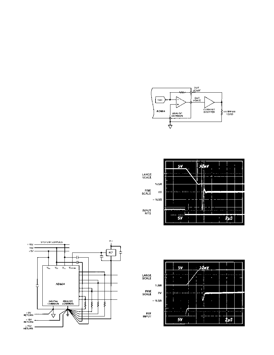
Figure 2. Recommended Circuit Schematic
greater than both the external reference and the inverted exter-
nal reference.
Output Considerations
Each DAC output can source or sink 5 mA of current to an
external load. Short-circuit protection limits load current to a
maximum load current of 40 mA. Load capacitance of up to
500 pF can be accommodated with no effect on stability.
Should an application require additional output current, a cur-
rent boosting element can be inserted into the output loop with
no sacrifice in accuracy. Figure 3 details this method.
Figure 3. Current-Boosting Scheme
AD664 output voltage settling time is 10
µ
s maximum. Figure 4
shows the output voltage settling time with a fixed 10 V refer-
ence, gain = 1 and all bits switched from 1 to 0.
Figure 4. Settling Time; All Bits Switched from On to Off
Alternately, Figure 5 shows the settling characteristics when the
reference is switched and the input bits remain fixed. In this
case, all bits are "on," the gain is 1 and the reference is switched
from ≠5 V to +5 V.
Figure 5. Settling Time; Input Bits Fixed, Reference
Switched
AD664
REV. C
≠7≠
Multiplying Mode Performance
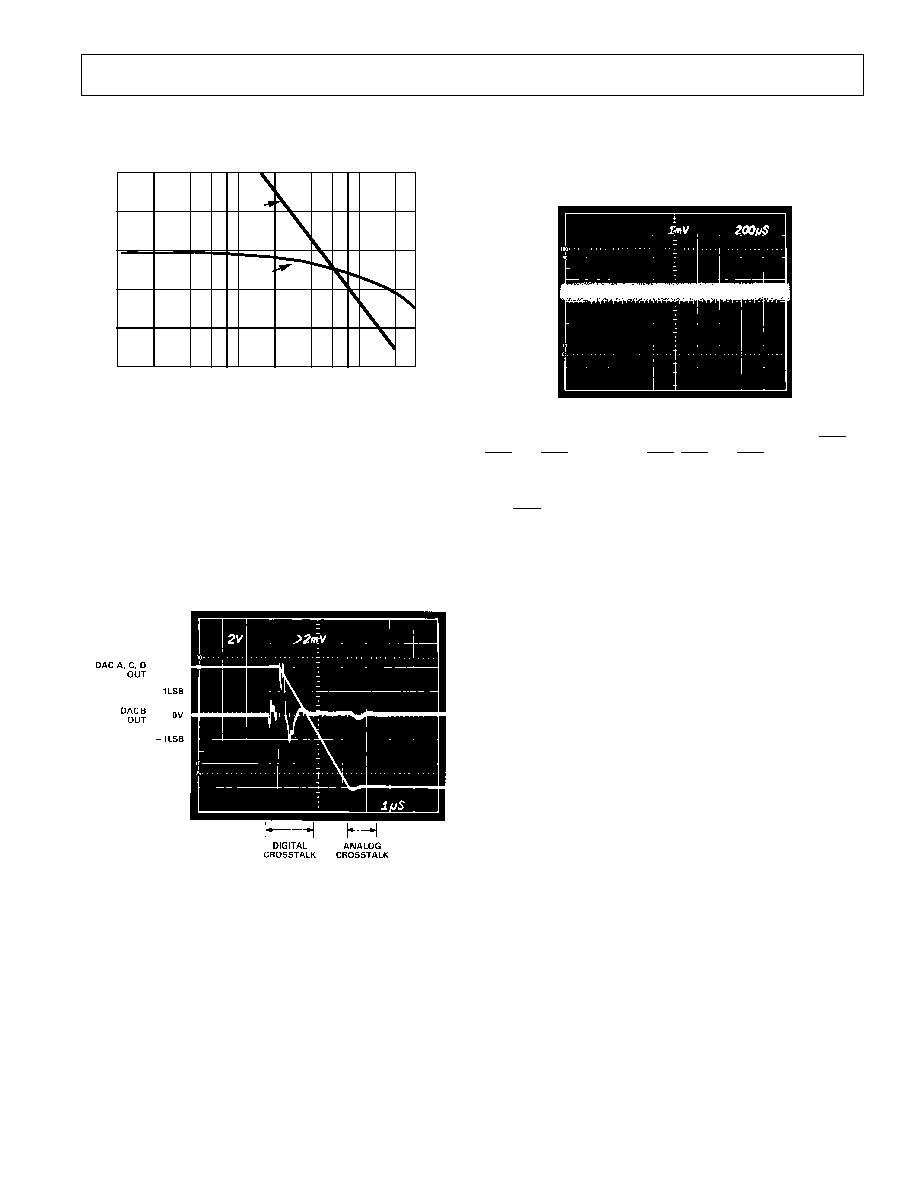
Figure 6 illustrates the typical open-loop gain and phase perfor-
mance of the output amplifiers of the AD664.
GAIN ≠ dB
0
+5
+20
+15
+10
10k
100k
1M
0
+45
+90
PHASE MARGIN ≠ Degrees
FREQUENCY ≠ H
z
GAIN
PHASE
Figure 6. Gain and Phase Performance of AD664 Outputs
Crosstalk
Crosstalk is a spurious signal on one DAC output caused by a
change in the output of one or more of the other DACs.
Crosstalk can be induced by capacitive, thermal or load current
induced feedthrough. Figure 7 shows typical crosstalk. DAC B
is set to output 0 volts. The outputs of DAC A, C and D switch
2 k
loads from 10 V to 0 V. The first disturbance in the output
of DAC B is caused by digital feedthrough from the input data
lows. The second disturbance is caused by analog feedthrough
from the other DAC outputs.
Figure 7. Output Crosstalk
Output Noise
Wideband output noise is shown in Figure 8. This measurement
was made with a 7 MHz noise bandwidth, gain = 1 and all bits
on. The total rms noise is approximately one fifth the visual
peak-to-peak noise.
DIGITAL INTERFACE
As Table II shows, the AD664 makes a wide variety of operating
modes available to the user. These modes are accessed or pro-
grammed through the high speed digital port of the quad DAC.
On-board registers program and store the DAC input codes and
the DAC operating mode data. All registers are double-buffered
to allow for simultaneous updating of all outputs. Register data
may be read back to verify the respective contents. The digital
port also allows transparent operation. Data from the input pins
can be sent directly through both ranks of latches to the DAC.
Figure 8. Typical Output Noise
Partial address decoding is performed by the DS0, DS1, QS0,
QS1
and QS2 address bits. QS0, QS1 and QS2 allow the 44-pin
versions of the AD664 to be addressed in 4-bit nibble, 8-bit byte
or 12-bit parallel words.
The RST pin provides a simple method to reset all output
voltages to zero. Its advantages are speed and low software
overhead.
INPUT DATA
In general, two types of data will be input to the registers of the
AD664, input code data and mode select data. Input code data
sets the DAC inputs while the mode select data sets the gain
and range of each DAC.
The versatile I/O port of the AD664 allows many different types
of data input schemes. For example, the input code for just one
of the DACs may be loaded and the output may or may not be
updated. Or, the input codes for all four DACs may be written,
and the outputs may or may not be updated.
The same applies for MODE SELECTION. The mode of just
one or many of the DACs may be rewritten and the user can
choose to immediately update the outputs or wait until a later
time to transfer the mode information to the outputs.
A user may also write both input code and mode information
into their respective first ranks and then update all second ranks
at once.
Finally, transparent operation allows data to be transferred from
the inputs to the outputs using a single control line. This feature
is useful, for example, in a situation where one of the DACs is
used in an A/D converter. The SAR register could be connected
directly to a DAC by using the transparent mode of operation.
Another use for this feature would be during system calibration
where the endpoints of the transfer function of each DAC would
be measured. For example, if the full-scale voltages of each
DAC were to be measured, then by making all four DACs
transparent and putting all "1s" on the input port, all four
DACs would be at full-scale. This requires far less software
overhead than loading each register individually.
AD664
REV. C
≠8≠
Table II. AD664 Digital Truth Table
Function
DS1, DS0
LS
MS
TR
QS0
, 1, 2
1
RD
CS
RST
Load 1st Rank (data)
DACA
00
0
1
1
Select Quad
1
1
0
1
DACB
01
0
1
1
Select Quad
1
1
0
1
DACC
10
0
1
1
Select Quad
1
1
0
1
DACD
11
0
1
1
Select Quad
1
1
0
1
Load 2nd Rank (data)
XX
1
1
1
XXX
1
1
0
1
Readback 2nd Rank (data)
Select D/A
X
1
1
Select Quad
0
1
0
1
Reset
XX
X
X
X
XXX
X
X
0
Transparent
1
All DACs
XX
1
1
0
000
1
1
0
1
DACA
00
0
1
0
000
1
1
0
1
DACB
01
0
1
0
000
1
1
0
1
DACC
10
0
1
0
000
1
1
0
1
DACD
11
0
1
0
000
1
1
0
1
Mode Select
1, 2
1st Rank
XX
0
0
1
00X
1
1
0
1
2nd Rank
XX
1
0
1
XXX
1
1
0
1
Readback Mode
1
XX
X
0
1
00X
0
1
0
1
Update 2nd Rank
and Mode
XX
1
0
0
XXX
1
1
0
1
NOTES
X = Don't Care.
1
For 44-pin versions only. Allow the AD664 to be addressed in 4-bit nibble, 8-bit byte or 12-bit parallel words.
2
For MS, TR, LS = 0, a MS 1st write occurs.
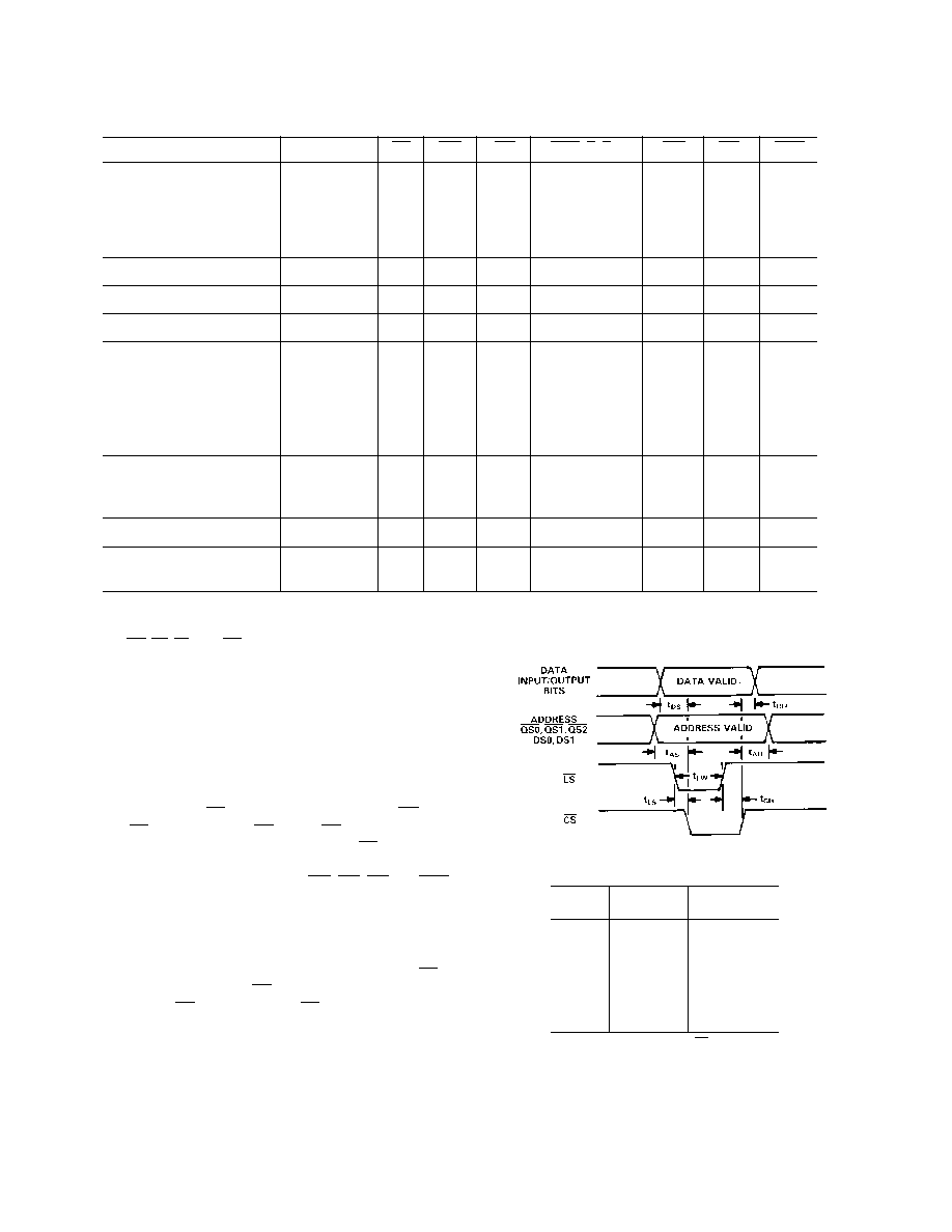
Figure 9a. Update Output of a Single DAC
25 C
T
MIN
to T
MAX
SYMBOL
MIN (ns)
MIN (ns)
t
LS
*
0
0
t
DS
0
0
t
DH
0
0
t
LW
60
80
t
CH
30
50
t
AS
0
0
t
AH
0
0
*FOR t
LS
> 0, THE WIDTH OF LS MUST BE
INCREASED BY THE SAME AMOUNT THAT
t
LS
IS GREATER THAN 0 ns.
Figure 9b. Update Output of a Single DAC Timing
The following sections detail the timing requirements for
various data loading schemes. All of the timing specifica-
tions shown assume V
IH
= 2.4 V, V
IL
= 0.4 V, V
CC
= +15 V,
V
EE
= ≠15 V and V
LL
= +5 V
.
Load and Update One DAC Output
In this first example, the object is simply to change the output of
one of the four DACs on the AD664 chip. The procedure is to
select the address bits that indicate the DAC to be programmed,
pull LATCH SELECT (LS) low, pull CHIP SELECT (CS)
low, release LS and then release CS. When CS goes low, data
enters the first rank of the input latch. As soon as LS goes high,
the data is transferred into the second rank and produces the
new output voltage. During this transfer, MS, TR, RD and RST
should be held high.
Preloading the First Rank of One DAC
In this case, the object is to load new data into the first rank of
one of the DACs but not the output. As in the previous case, the
address and data inputs are placed on the appropriate pins. LS
is then brought to "0" and then CS is asserted. Note that in this
situation, however, CS goes high before LS goes high. The in-
put data is prevented from getting to the second rank and affect-
ing the output voltage.
AD664
REV. C
≠9≠
Figure 10a. Preload First Rank of a DAC
25 C
T
MIN
to T
MAX
SYMBOL
MIN (ns)
MIN (ns)
t
LS
0
0
t
LH
15
15
t
CW
80
100
t
DS
0
0
t
DH
15
15
t
AS
0
0
t
AH
15
15
Figure 10b. Preload First Rank of a DAC Timing
This allows the user to "preload" the data to a DAC and strobe
it into the output latch at some future time. The user could do
this by reproducing the sequence of signals illustrated in the
next section.
Update Second Rank of a DAC
Assuming that a new input code had previously been placed into
the first rank of the input latches, the user can update the out-
put of the DAC by simply pulling CS low while keeping LS,
MS
, TR, RD and RST high. Address data is not needed in this
case. In reality, all second ranks are being updated by this pro-
cedure, but only those which receive data different from that
already there would manifest a change. Updating the second
rank does not change the contents of the first rank.
Figure 11. Update Second Rank of a DAC
The same options that exist for individual DAC input loading
also exist for multiple DAC input loading. That is, the user can
choose to update the first and second ranks of the registers or
preload the first ranks and then update them at a future time.
Preload Multiple First Rank Registers
The first ranks of the DAC input registers may be preloaded
with new input data without disturbing the second rank data.
This is done by transferring the data into the first rank by bring-
ing CS low while LS is low. But CS must return high before LS.
This prevents the data from the first rank from getting into the
second rank. A simple second rank update cycle as shown in
Figure 11 would move the "preloaded" information to the
DACs.
Figure 12. Preload First Rank Registers
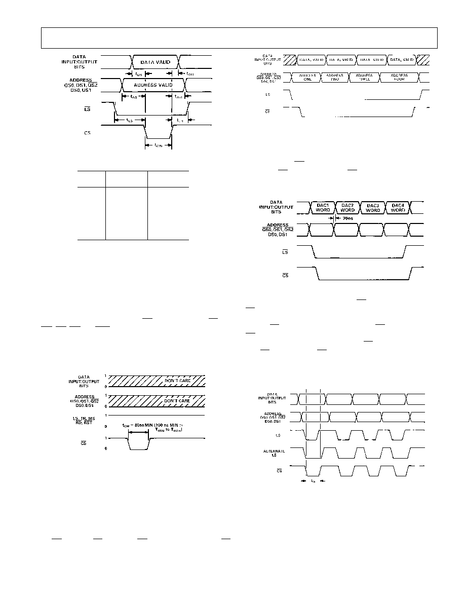
Load and Update Multiple DAC Outputs
The following examples demonstrate two ways to update all
DAC outputs. The first method involves doing all data transfers
during one long CS low period. Note that in this case, shown in
Figure 13, LS returns high before CS goes high. Data hold time,
relative to an address change, is 70 ns. This updates the outputs
of all DACs simultaneously.
Figure 13. Update All DAC Outputs
The second method involves doing a CS assertion (low) and an
LS
toggle separately for each DAC. It is basically a series of
preload operations (Figure 10). In this case, illustrated in Figure
14, two LS signals are shown. One, labeled LS, goes high before
CS
returns high. This transfers the "new" input word to the
DAC outputs sequentially. The second LS signal, labeled Alter-
nate LS, stays low until CS returns high. Using this sequence
loads the first ranks with each "new" input word but doesn't up-
date the DAC outputs. To then update all DAC outputs simul-
taneously would require the signals illustrated in Figure 11.
Figure 14. Load and Update Multiple DACs
SELECTING GAIN RANGE AND MODES (44-PIN
VERSIONS)
The AD664's mode select feature allows a user to configure the
gain ranges and output modes of each of the four DACs.
On-board switches take the place of up to eight external relays
that would normally be required to accomplish this task. The
switches are programmed by the mode select word entered via
the data I/O port. The mode select word is eight-bits wide and
AD664
REV. C
≠10≠
occupies the topmost eight bits of the input word. The last four
bits of the input word are "don't cares."
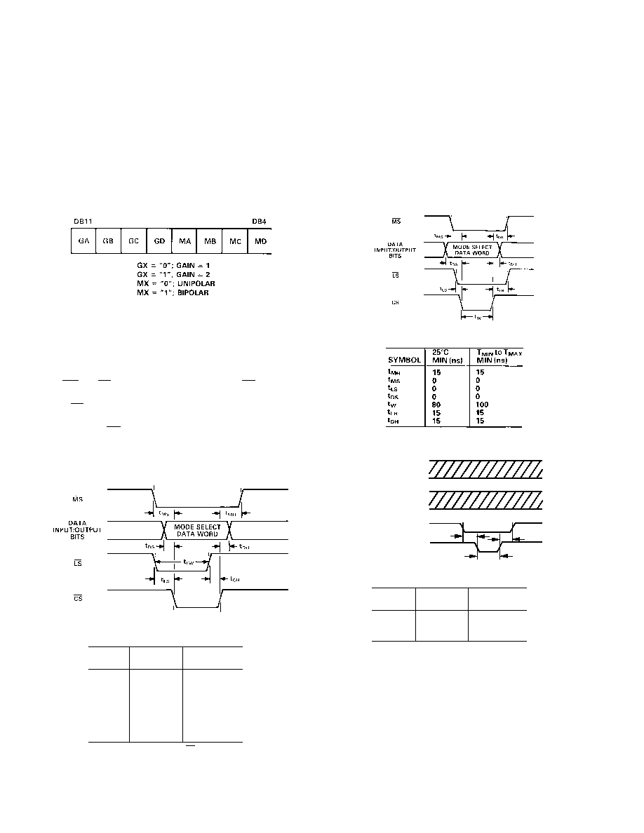
Figure 15 shows the format of the MODE SELECT word. The
first four bits determine the gain range of the DAC. When set to
be a gain of 1, the output of the DAC spans a voltage of 1 times
the reference. When set to a gain of 2, the output of the DAC
spans a voltage of 2 times the reference.
The next four bits determine the mode of the DAC. When set to
UNIPOLAR, the output goes from 0 to REF or 0 to 2 REF.
When the BIPOLAR mode is selected, the output goes from
≠REF/2 to REF/2 or ≠REF to REF.
Figure 15. Mode Select Word Format
Load and Update Mode of One DAC
In this next example, the object is to load new mode informa-
tion for one of the DACs into the first rank of latches and then
immediately update the second rank. This is done by putting the
new mode information (8-bit word length) onto the databus.
Then MS and LS are pulled low. Following that, CS is pulled
low. This loads the mode information into the first rank of
latches. LS is then brought high. This action updates the second
rank of latches (and, therefore, the DAC outputs). The load
cycle ends when CS is brought high.
In reality, this load cycle really updates the modes of all the
DACs, but the effect is to only change the modes of those
DACs whose mode select information has actually changed.
Figure 16a. Load and Update Mode of One DAC
25 C
T
MIN
to T
MAX
SYMBOL
MIN (ns)
MIN (ns)
t
MS
0
0
t
LS
*
0
0
t
DS
0
0
t
LW
60
70
t
CH
70
80
t
DH
0
0
t
MH
0
0
*FOR t
LS
> 0, THE WIDTH OF LS MUST BE
INCREASED BY THE SAME AMOUNT THAT
t
LS
IS GREATER THAN 0 ns.
Figure 16b. Load and Update Mode of One DAC Timing
Preloading the Mode Select Register
Mode data can be written into the first rank of the mode select
latch without changing the modes currently being used. This
feature is useful when a user wants to preload new mode infor-
mation in anticipation of strobing that in at a future time. Fig-
ure 17 illustrates the correct sequence and timing of control
signals to accomplish this task.
This allows the user to "preload" the data to a DAC and strobe
it into the output latch at some future time. The user could do
this by reproducing the sequence of signals illustrated in Figures
17c and 17d.
Figure 17a. Preload Mode Select Register
Figure 17b. Preload Mode Select Register Timing
1
0
1
0
DATA
INPUT/OUTPUT
BITS
ADDRESS
QS0,QS1,QS2
DS0,DS1
___
___
___
__
MS
__
CS
t
MS
t
MH
t
W
Figure 17c. Update Second Rank of Mode Select Latch
25 C
T
MIN
to T
MAX
SYMBOL
MIN (ns)
MIN (ns)
t
MS
0
0
t
MH
0
0
t
W
80
100
Figure 17d. Update Second Rank of Mode Select Latch
Timing
Transparent Operation (44-Pin Versions)
Transparent operation allows data from the inputs of the
AD664 to be transferred into the DAC registers without the
intervening step of being latched into the first rank of latches.
Two modes of transparent operation exist, the "partially trans-
parent" mode and a "fully transparent" mode. In the "partially
transparent" mode, one of the DACs is transparent while the
remaining three continue to use the data latched into their
respective input registers. Both modes require a 12-bit wide
input word!
AD664
REV. C
≠11≠
OUTPUT DATA
Two types of outputs may be obtained from the internal data
registers of the AD664 chip, mode select and DAC input code
data. Readback data may be in the same forms in which it can
be entered; 4-, 8-, and 12-bit wide words (12 bits only for
28-pin versions).
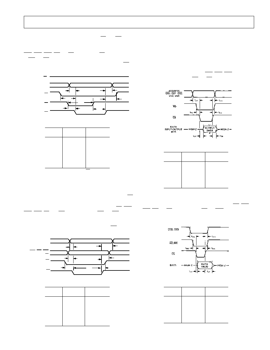
DAC Data Readback
DAC input code readback data is obtained by setting the address
of the DAC (DS0, DS1) and Quads (QS0, QS1, QS2) on the
address pins and bringing the RD and CS pins low. The timing
diagram for a DAC code readback operation appears in Figure 20.
Figure 20a. DAC Input Code Readback
25
∞
C
T
MIN
to T
MAX
SYMBOL
MIN (ns)
MIN (ns)
t
AS
0
0
t
RS
0
0
t
DV
150
180
t
DF
60
75
t
AH
0
0
t
RH
0
0
Figure 20b. DAC Input Code Readback Timing
Mode Data Readback
Mode data is read back in a similar fashion. By setting MS, QS0,
QS1
, RD and CS low while setting TR and RST high, the mode
select word is presented to the I/O port pins. Figure 21 shows the
timing diagram for a readback of the mode select data register.
Figure 21a. Mode Data Readback
25 C
T
MIN
to T
MAX
SYMBOL
MIN (ns)
MIN (ns)
t
AS
0
0
t
MS
0
0
t
DV
150
180
t
DF
60
75
t
AH
0
0
t
MH
0
0
Figure 21b. DAC Mode Readback Timing
Fully transparent operation can be thought of as a simultaneous
load of data from Figure 9a where replacing LS with TR causes
all 4 DACs to be loaded at once.
The Fully transparent mode is achieved by asserting lows on
QS0
, QS1, QS2, TR and CS while keeping LS high in addition
to MS and RB. Figure 18a illustrates the necessary timing rela-
tionships. Fully transparent operation will also work with TR
tied low (enabled).
DATA INPUT/
OUTPUT BITS
t
TS
t
DS
t
QH
t
DH
t
QS
DATA VALID
TW
t
t
CH
1
LS
QS
TR
CS
Figure 18a. Fully Transparent Mode
25 C
T
MIN
to T
MAX
SYMBOL
MIN (ns)
MIN (ns)
t
AS
0
0
t
QS
0
0
t
TS
*
0
0
t
TW
80
90
t
CH
90
110
t
DH
0
0
t
QH
0
0
*FOR t
TS
> 0, THE WIDTH OF TR MUST BE
INCREASED BY THE SAME AMOUNT THAT
t
TS
IS GREATER THAN 0 ns.
Figure 18b. Fully Transparent Mode Timing
Partially transparent operation can be thought of as preloading
the first rank in Figure 10a without requiring the additional CS
pulse from Figure 11.
The partially transparent mode is achieved by setting CS, QS0,
QS1
, QS2, LS, and TR low while keeping RD and MS high.
The address of the transparent DAC is asserted on DS0 and
DS1. Figure 19a illustrates the necessary timing relationships.
Partially transparent operation will also work with TR tied low
(enabled).
DATA INPUT/
OUTPUT BITS
ADDRESS
QS0, QS1, QS2
DS0, DS1, LS
t
TS
t
AS
t
DH
DATA VALID
W
t
t
TH
TR
CS
ADDRESS VALID
t
AH
t
DS
Figure 19a. Partially Transparent
25
∞
C
T
MIN
to T
MAX
SYMBOL
MIN (ns)
MIN (ns)
t
DS
0
0
t
AS
0
0
t
TS
0
0
t
W
90
110
t
DH
15
15
t
AH
15
15
t
TH
15
15
Figure 19b. Partially Transparent Mode Timing

AD664
REV. C
≠12≠
Output Loads
Readback timing is tested with the output loads shown in Figure
22.
Figure 22. Output Loads
Asynchronous Reset Operation
The asynchronous reset signal shown in Figure 23 may be
asserted at any time. A minimum pulse width (t
RW
) of 90 ns is
required. The reset feature is designed to return all DAC out-
puts to 0 volts regardless of the mode or range selected. In the
44-pin versions, the modes are reset to unipolar 10 V span (gain
of 1), and the input codes are rewritten to be "0s." Previous
DAC code and mode information is erased.
Figure 23a. Asynchronous Reset Operation
Figure 23b. Asynchronous Reset Operation Timing
In the 28-pin versions of the AD664, the mode remains
unchanged, the appropriate input code is rewritten to reset the
output voltage to 0 volts. As in the 44-pin versions, the previous
input data is erased.
At power-up, an AD664 may be activated in either the read or
write modes. While at the device level this will not produce any
problems, at the system level it may. Analog Devices recom-
mends the addition of a simple power-on reset scheme to any
system where the possibility of an unknown start-up state could
be a problem. The simplest version of this scheme is illustrated
in Figure 24.
AD664
AD664
+5V
10k
100nF
#1
RST
#N
RST
Figure 24. Power-On Reset
It is obvious from inspection that the scheme shown in Figure
24 is only appropriate for systems in which the RST is otherwise
not used. Should the user wish to use the RST pin, an addi-
tional logic gate may be included to combine the power-on reset
with the reset signal.
INTERFACING THE AD664 TO MICROPROCESSORS
The AD664 is easy to interface with a wide variety of popular
microprocessors. Common architectures include processors with
dedicated 8-bit data and address buses, an 8-bit bus over which
data and address are multiplexed, an 8-bit data and 16-bit
address partially muxed, and separate 16-bit data and address
buses.
AD664 addressing can be accomplished through either
memory-mapped or I/O techniques. In memory-mapped
schemes, the AD664 appears to the host microprocessor as
RAM memory. Standard memory addressing techniques are
used to select the AD664. In the I/O schemes, the AD664 is
treated as an external I/O device by the host. Dedicated I/O pins
are used to address the AD664.
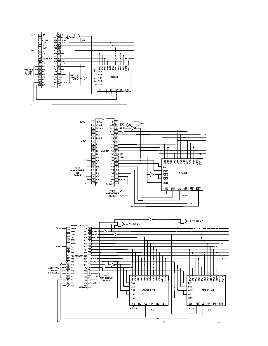
MC6801 Interface
In Figures 25a≠25d, we illustrate a few of the various methods
that can be used to connect an AD664 to the popular MC6801
microprocessor. In each of these cases, the MC6801 is intended
to be configured in its expanded, nonmultiplexed mode of
operation. In this mode, the MC6801 can address 256 bytes of
external memory over 8-bit data (Port 3) and 8-bit address
(Port 4) buses. Eight general-purpose I/O lines (Port 1) are also
available. On-board RAM and ROM provide program and data
storage space.
In Figure 25a, the three least significant address bits (P40, P41
and P42) are employed to select the appropriate on-chip
addresses for the various input registers of the AD664. Three
I/O lines (P17, P16 and P15) are used to select various operat-
ing features of the the AD664. IOS and E(nable) are combined
to produce an appropriate CS signal. This addressing scheme
leaves the five most significant address bits and five I/O lines
free for other tasks in the system.
Figure 25b shows another way to interface an AD664 to the
MC6801. Here we've used the six least significant address lines
to select AD664 features and registers. This is a purely memory-
mapped scheme while the one illustrated in Figure 25a uses
some memory-mapping as well as some dedicated I/O pins. In
Figure 25b, two address lines and all eight I/O lines remain free
for other system tasks.
AD664
REV. C
≠13≠
Figure 25a. Simple AD664 to MC6801 Interface
Expansion of the scheme employed in Figure 25a results in that
shown in Figure 25c. Here, two AD664s are connected to an
MC6801, providing a total of eight 12-bit, software program-
mable DACs. Again, the three least significant bits of address
are used to select the on-chip registers of the AD664. IOS and
E, as well as a fourth address bit, are decoded to provide the
appropriate CS signals. Four address and five I/O lines remain
uncommitted.
A slightly more sophisticated approach to system expansion is
illustrated in Figure 25d. Here, a 74LS138 (1-of-8 decoder) is
used to address one of the eight AD664s connected to the
MC6801. The three least significant address bits are used to
select on-chip register and DAC. The next three address bits are
used to select the appropriate AD664. IOS and E gate the
74LS138 output.
Figure 25b. Alternate AD664 to MC6801 Interface
Figure 25c. Interfacing Two AD664s to an MC6801

AD664
REV. C
≠14≠
The schemes in Figure 25 illustrate some of the trade-offs which
a designer may make when configuring a system. For example,
the designer may use I/O lines instead of address bits or vice
versa. This decision may be influenced by other I/O tasks or sys-
tem expansion requirements. He/she can also choose to imple-
ment only a subset of the features available. Perhaps the RST
pin isn't really needed. Tying that input pin to V
LOGIC
frees up
another I/O or address bit. The same consideration applies to
mode select. In all of these cases TR is shown tied to V
LOGIC
,
because the MC6801 cannot provide the 12-bit-wide input
word required for the transparent mode. In situations where
transparent operation isn't required, and mode select is also not
needed, the designer may consider specifying the DIP version of
the device (either the UNI or BIP version).
Each of the schemes illustrated in Figure 25 operates with an
MC6801 at clock rates up to and including 1.5 MHz. Similar
schemes can be derived for other 8-bit microprocessors and
microcontrollers such as the 8051/8086/8088/6502, etc. One
such scheme developed for the 8051/AD664 is illustrated in
Figure 26.
8051 Interface
Figure 26 shows the AD664 combined with an 8051
µ
controller
chip. Three LSBs of address provide the quad and DAC select
signals. Control signals from Port 1 select various operating
modes such as readback, mode select and reset as well as pro-
viding the LS signal. Read and write signals from the 8051 are
decoded to provide the CS signal.
Figure 25d. Interfacing Eight AD664s to an MC6801

AD664
REV. C
≠15≠
IBM PC* Interface
Figure 27 illustrates a simple interface between an IBM PC and
an AD664. The three least significant address bits are used to
select the Quad and DAC. The next two address bits are used
for LS and MS. In this scheme, a 12-bit input word requires
two load cycles, an 8-bit word and a 4-bit word. Another write
is required to transfer the word or words previously written to
the second rank. A 12-bit-wide word again requires at least two
read cycles; one for the 8 MSBs and four for the LSBs. The
page select signal produces a CS strobe for any address from
300H to 31FH.
Figure 26. AD664 to 8051 Interface
Figure 27. AD664 to IBM PC Interface
*IBM PC is a trademark of International Business Machines Corp.
AD664
REV. C
≠16≠
Table III details the memory locations and addresses used by this interface.
Table III. IBM PC Memory Map
HEX
A9
A8
A7
A6
A5
A4
A3
A2
A1
A0
REGISTER SELECTED
300
1
1
0
0
0
0
0
0
0
0
Illegal Address
301
0
0
1
Mode Select, 1st Rank
302
0
1
0
Illegal Address
303
0
1
1
Mode Select, 1st Rank
304
1
0
0
Illegal Address
305
1
0
1
Mode Select, 1st Rank
306
1
1
0
Illegal Address
307
w
1
1
1
Mode Select, 1st Rank
308
1
0
0
0
Mode Select, 2nd Rank
309
0
0
1
30A
0
1
0
30B
0
1
1
30C
1
0
0
30D
1
0
1
30E
1
1
0
30F
w
w
1
1
1
w
310
1
0
0
0
0
DAC A, 4 LSBs, 1st Rank
311
0
0
1
DAC A, 8 MSBs, 1st Rank
312
0
1
0
DAC B, 4 LSBs, 1st Rank
313
0
1
1
DAC B, 8 MSBs, 1st Rank
314
1
0
0
DAC C, 4 LSBs, 1st Rank
315
1
0
1
DAC C, 8 MSBs, 1st Rank
316
1
1
0
DAC D, 4 LSBs, 1st Rank
317
w
1
1
1
DAC D, 8 MSBs, 1st Rank
318
1
0
0
0
2nd Rank
319
0
0
1
31A
0
1
0
31B
0
1
1
31C
1
0
0
31D
1
0
1
31E
1
1
0
31F
w
w
w
w
w
w
w
1
1
1
w
Note: Shaded registers are readable.

AD664
REV. C
≠17≠
The following IBM PC Basic routine produces four output volt-
age ramps from one AD664. Line numbers 10 through 70 de-
fine the hardware addresses for the first and second ranks of
DAC registers as well as the first and second ranks of the mode
select register. Program variables are initialized in line numbers
110 through 130. Line number 170 writes "0s" out to the first
rank and, then, the second rank of the mode select register.
Line numbers 200 through 320 calculate output voltages. Fi-
nally line numbers 410 through 450 update the first, then the
second ranks of the DAC input registers. Hardware registers
may be read with the "INP" instruction. For example, the con-
tents of the DAC A register may be accessed with the following
com mand: Line#
A = INP(DACA).
5
REM----AD664 LISSAJOUS PATTERNS----
10
REM ---ASSIGN HARDWARE ADDRESSES---
20
DACA = 785
30
DACB = 787
40
DACC = 789
50
DACD = 791
60
DAC2ND = 792
70
MODE1 = 769: MODE2 = 776
80
REM
90
REM
100
REM ---INITIALIZE VARIABLES---
110
X = 0: Y1 = 128: Y2 = 64: Y3 = 32
120
CX = 1: CY1 = 1: CY2 = -1: CY3= 1
130
FX = 9: FY1 = 5: FY2 = 13: FY3 = 15
140
REM
150
REM
160
REM ---INITIALIZE MODES AND GAINS---
170
OUT MODE1,0: OUT MODE2,0
180
REM
190
REM
200
REM ---CALCULATE VARIABLES---
210
X = X + FX*CX
220
Y1 = Y1 + FY1*CY1
230
Y2 = Y2 + FY2*CY2
240
Y3 = Y3 + FY3*CY3
250
IF X > 255 THEN X = 255: CX = -1: GOTO 270
260
IF X < 0 THEN X = 0: CX = 1
270
IF Y1 > 255 THEN Y1 = 255: CY1 = -1: GOTO 290
280
IF Y1 < 0 THEN Y1 = 0: CY1 = 1
290
IF Y2 > 255 THEN Y2 = 255: CY2 = -1 GOTO 310
300
IF Y2 < 0 THEN Y2 = 0: CY2 = -1
310
IF Y3 > 255 THEN Y3 = 255: CY3 = -1: GOTO 400
320
IF Y3 < 0 THEN Y3 = 0: CY3 = 1
330
REM
340
REM
400
REM ---SEND DAC DATA---
410
OUT DACA,X
420
OUT DACB,Yl
430
OUT DACC,Y2
440
OUT DACD,Y3
450
OUT DAC2ND,0
500
REM
510
REM
520
REM ---LOOP BACK---
530
GOTO 210

AD664
REV. C
≠18≠
Simple AD664 to MC68000 Interface
Figure 28 shows an AD664 connected to an MC68000. In this
memory-mapped I/O scheme, the "left-justified" data is written
in one 12-bit input word. Four address bits are used to perform
the on-chip D/A selection as well as the various operating fea-
tures. The R/W signal controls the RD function and system
reset controls RST.
This scheme can be converted to write "right-justified'' data by
connecting the data inputs to DATA bits D0 through D11
respectively. Other options include controlling the QS0, QS1
and QS2 pins with UDS and LDS to provide a way to write
8-bit input and read 8-bit output words.
Figure 28. AD664 to MC68000 Interface

AD664
REV. C
≠19≠
Figure 29. AD664 in "Tester-per-Pin" Architecture
APPLICATIONS OF THE AD664
"Tester-Per-Pin" ATE Architecture
Figure 29 shows the AD664 used in a single channel of a digital
test system. In this scheme, the AD664 supplies four individual
output voltages. Two are provided to the V
HIGH
and V
LOW
in-
puts of the AD345 pin driver I.C. to set the digital output levels.
Two others are routed to the inputs of the AD96687 dual com-
parator to supply reference levels of the readback features. This
approach can be replicated to give as many channels of stimulus/
readback as the tester has pins. The AD664 is a particularly
appropriate choice for a large-scale system because the low
power requirements (under 500 mW) ease power supply and
cooling requirements. Analog ground currents of 600
µ
A or less
make the ground current management task simpler. All DACs
can be driven from the same system reference and will track
over time and temperature. Finally, the small board area
required by the AD664 (and AD345 and AD96687) allows a
high functional density.
X-Y Plotters
Figure 30 is a block diagram of the control section of a
microprocessor-controlled X-Y pen plotter. In this conceptual
exercise, two of the DACs are used for the X-channel drive and
two are used for the Y-channel drive. Each provides either the
coarse or fine movement control for its respective channel. This
approach offers increased resolution over some other approaches.
A designer can take advantage of the reset feature of the AD664
in the following manner. If the system is designed such that the
"HOME" position of the pen (or galvanometer, beam, head or
similar mechanism) results when the outputs of all of the DACs
are at zero, then no system software is required to home the
pen. A simple reset signal is sufficient.
Similarly, the transparent feature could be used to the same
end. One code can be sent to all DACs at the same time to send
the pen to the home position. Of course, this would require
some software where the previous example would require only a
single reset strobe signal!
Drawing scaling can be achieved by taking advantage of the
AD664's software programmable gain settings. If, for example,
an "A" size drawing is created with gain settings of 1, then a
"C" size drawing can be created by simply resetting all DAC
gains to 2 and redrawing the object. Conversely, a "C" size
drawing created with gains of 2 can be reduced to "A" size sim-
ply by changing the gains to 1 and redrawing. The same princi-
pal applies for conversion from "B" size to "D" size or "D" size
to "B" size. The multiplying capability of the AD664 provides
another scaling option. Changing the reference voltage provides
a proportional change in drawing size. Inverting the reference
voltage would invert the drawing.
Swapping digital input data from the X channel to the Y chan-
nel would rotate the drawing 90 degrees.
Figure 30. X-Y Plotter Block Diagram
AD664
REV. C
≠20≠
PRINTED IN U.S.A.
C1159c≠20≠12/91
ORDERING GUIDE
Temperature
Gain
Linearity
Package
Model
l
Range
Output Range
Error
Error
Options
2
AD664JN-UNI
0
∞
C to +70
∞
C
0 to +V
REF
±
7 LSB
±
0.75 LSB
N-28
AD664JN-BIP
0
∞
C to +70
∞
C
≠V
REF
to +V
REF
±
7 LSB
±
0.75 LSB
N-28
AD664JP
0
∞
C to +70
∞
C
Programmable
±
7 LSB
±
0.75 LSB
P-44A
AD664KN-UNI
0
∞
C to +70
∞
C
0 to +V
REF
±
5 LSB
±
0.5 LSB
N-28
AD664KN-BIP
0
∞
C to +70
∞
C
≠V
REF
to +V
REF
±
5 LSB
±
0.5 LSB
N-28
AD664KP
0
∞
C to +70
∞
C
Programmable
±
5 LSB
±
0.5 LSB
P-44A
AD664AD-UNI
≠40
∞
C to +85
∞
C
0 to +V
REF
±
7 LSB
±
0.75 LSB
D-28
AD664AD-BIP
≠40
∞
C to +85
∞
C
≠V
REF
to +V
REF
±
7 LSB
±
0.75 LSB
D-28
AD664AJ
≠40
∞
C to +85
∞
C
Programmable
±
7 LSB
±
0.75 LSB
J-44
AD664BD-UNI
≠40
∞
C to +85
∞
C
0 to +V
REF
±
5 LSB
±
0.5 LSB
D-28
AD664BD-BIP
≠40
∞
C to +85
∞
C
≠V
REF
to +V
REF
±
5 LSB
±
0.5 LSB
D-28
AD664BJ
≠40
∞
C to +85
∞
C
Programmable
±
5 LSB
±
0.5 LSB
J-44
AD664BE
≠40
∞
C to +85
∞
C
Programmable
±
5 LSB
±
0.5 LSB
E-44A
AD664SD-UNI
≠55
∞
C to +125
∞
C
0 to +V
REF
±
7 LSB
±
0.75 LSB
D-28
AD664SD-BIP
≠55
∞
C to +125
∞
C
≠V
REF
to +V
REF
±
7 LSB
±
0.75 LSB
D-28
AD664TD-UNI
≠55
∞
C to +125
∞
C
0 to +V
REF
±
5 LSB
±
0.5 LSB
D-28
AD664TD-BIP
≠55
∞
C to +125
∞
C
≠V
REF
to +V
REF
±
5 LSB
±
0.5 LSB
D-28
NOTES
1
For details on grade and package offerings screened in accordance with MIL-STD-883, refer to the Analog Devices Military Products Databook or current
AD664/883B data sheet.
2
D = Ceramic DIP; E = Leadless Ceramic Chip Carrier; J = Leaded Chip Carrier; N = Plastic DIP; P = Plastic Leaded Chip Carrier.
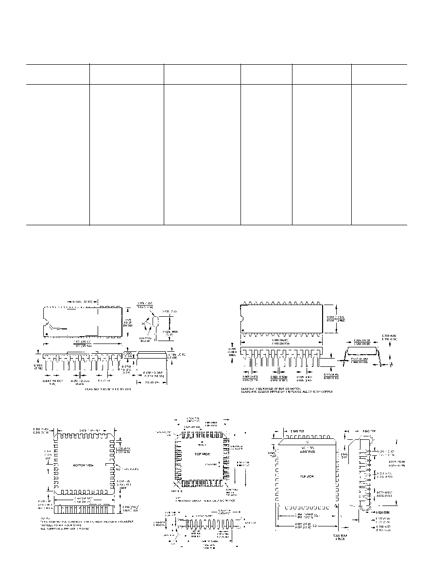
OUTLINE DIMENSIONS
Dimensions shown in inches and (mm).
N-28
28-Lead Plastic DIP
E-44A
44-Pin LCC Package
P-44A
44-Lead Plastic Leaded Chip Carrier (PLCC)
J-44
J-Leaded Chip Carrier
D-28
28-Pin Ceramic DIP Package