 | ÐлекÑÑоннÑй компоненÑ: AD6640 | СкаÑаÑÑ:  PDF PDF  ZIP ZIP |
Äîêóìåíòàöèÿ è îïèñàíèÿ www.docs.chipfind.ru
a
12-Bit, 65 MSPS
IF Sampling A/D Converter
FEATURES
65 MSPS Minimum Sample Rate
80 dB Spurious-Free Dynamic Range
IF-Sampling to 70 MHz
710 mW Power Dissipation
Single +5 V Supply
On-Chip T/H and Reference
Twos Complement Output Format
3.3 V or 5 V CMOS-Compatible Output Levels
APPLICATIONS
Cellular/PCS Base Stations
Multichannel, Multimode Receivers
GPS Anti-Jamming Receivers
Communications Receivers
Phased Array Receivers
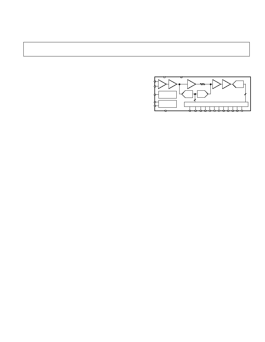
FUNCTIONAL BLOCK DIAGRAM
ADC
A
TH3
DAC
ADC
TH2
BUF
TH1
MSB
LSB
D11
D10 D9 D8 D7 D6 D5 D4 D3 D2 D1 D0
DIGITAL ERROR CORRECTION LOGIC
7
GND
6
AIN
AIN
V
REF
ENCODE
ENCODE
+2.4V
REFERENCE
INTERNAL
TIMING
AV
CC
DV
CC
AD6640
PRODUCT DESCRIPTION
The AD6640 is a high speed, high performance, low power,
monolithic 12-bit analog-to-digital converter. All necessary
functions, including track-and-hold (T/H) and reference are
included on-chip to provide a complete conversion solution.
The AD6640 runs on a single +5 V supply and provides CMOS-
compatible digital outputs at 65 MSPS.
Specifically designed to address the needs of multichannel,
multimode receivers, the AD6640 maintains 80 dB spurious-
free dynamic range (SFDR) over a bandwidth of 25 MHz.
Noise performance is also exceptional; typical signal-to-noise
ratio is 68 dB.
The AD6640 is built on Analog Devices' high speed complemen-
tary bipolar process (XFCB) and uses an innovative multipass
architecture. Units are packaged in a 44-terminal Plastic Thin
Quad Flatpack (TQFP) specified from 40
°
C to +85
°
C.
PRODUCT HIGHLIGHTS
1. Guaranteed sample rate is 65 MSPS.
2. Fully differential analog input stage specified for frequencies
up to 70 MHz; enables "IF Sampling."
3. Low power dissipation: 710 mW off a single +5 V supply.
4. Digital outputs may be run on +3.3 V supply for easy inter-
face to digital ASICs.
5. Complete Solution: reference and track-and-hold.
6. Packaged in small, surface mount, plastic 44-terminal TQFP.
AD6640
REV. 0
Information furnished by Analog Devices is believed to be accurate and
reliable. However, no responsibility is assumed by Analog Devices for its
use, nor for any infringements of patents or other rights of third parties
which may result from its use. No license is granted by implication or
otherwise under any patent or patent rights of Analog Devices.
One Technology Way, P.O. Box 9106, Norwood, MA 02062-9106, U.S.A.
Tel: 781/329-4700
World Wide Web Site: http://www.analog.com
Fax: 781/326-8703
© Analog Devices, Inc., 1998

DC SPECIFICATIONS
Test
AD6640AST
Parameter
Temp
Level
Min
Typ
Max
Units
RESOLUTION
12
Bits
ACCURACY
No Missing Codes
+25
°
C
I
GUARANTEED
Offset Error
Full
VI
10
3.5
+10
mV
Gain Error
Full
VI
10
4.0
+10
% FS
Differential Nonlinearity (DNL)
1
+25
°
C
I
1.0
±
0.5
+1.5
LSB
Integral Nonlinearity (INL)
1
Full
V
±
1.25
LSB
TEMPERATURE DRIFT
Offset Error
Full
V
50
ppm/
°
C
Gain Error
Full
V
100
ppm/
°
C
POWER SUPPLY REJECTION (PSRR)
Full
V
±
0.5
mV/V
REFERENCE OUT (V
REF
)
2
Full
V
2.4
V
ANALOG INPUTS (AIN,
AIN)
3
Analog Input Common-Mode Range
4
Full
V
V
REF
±
0.05
V
Differential Input Voltage Range
Full
V
2.0
V p-p
Differential Input Resistance
Full
IV
0.7
0.9
1.1
k
Differential Input Capacitance
+25
°
C
V
1.5
pF
POWER SUPPLY
Supply Voltage
AV
CC
Full
VI
4.75
5.0
5.25
V
DV
CC
Full
VI
3.0
3.3
5.25
V
Supply Current
IA
VCC
(AV
CC
= 5.0 V)
Full
VI
135
160
mA
ID
VCC
(DV
CC
= 3.3 V)
Full
VI
10
20
mA
POWER CONSUMPTION
Full
VI
710
865
mW
NOTES
1
ENCODE = 20 MSPS
2
If V
REF
is used to provide a dc offset to other circuits, it should first be buffered.
3
The AD6640 is designed to be driven differentially. Both AIN and
AIN should be driven at levels V
REF
±
0.5 volts. The input signals should be 180 degrees out of phase to
produce a 2 V p-p differential input signal. See Driving the Analog Inputs section for more details.
4
Analog input common-mode range specifies the offset range the analog inputs can tolerate in dc-coupled applications (see Figure 35 for more detail).
Specifications subject to change without notice
.
DIGITAL SPECIFICATIONS
Test
AD6640AST
Parameter
Temp
Level
Min
Typ
Max
Units
LOGIC INPUTS (ENC,
ENC)
1
Encode Input Common-Mode Range
2
Full
IV
0.2
2.2
V
Differential Input Voltage
Full
IV
0.4
V p-p
Single-Ended Encode
10
V p-p
Logic Compatibility
3
TTL/CMOS
Logic "1" Voltage
Full
VI
2.0
5.0
V
Logic "0" Voltage
Full
VI
0
0.8
V
Logic "1" Current (V
INH
= 5 V)
Full
VI
500
650
800
µ
A
Logic "0" Current (V
INL
= 0 V)
Full
VI
400
320
200
µ
A
Input Capacitance
+25
°
C
V
2.5
pF
LOGIC OUTPUTS (
D11D0)
4
Logic Compatibility
CMOS
Logic "1" Voltage (DV
CC
= +3.3 V)
Full
VI
2.8
DV
CC
0.2
V
Logic "0" Voltage (DV
CC
= +3.3 V)
Full
VI
0.2
0.5
V
Logic "1" Voltage (DV
CC
= +5.0 V)
Full
IV
4.5
DV
CC
0.3
V
Logic "0" Voltage (DV
CC
= +5.0 V)
Full
IV
0.35
0.5
V
Output Coding
Twos Complement
NOTES
1
Best dynamic performance is obtained by driving ENC and
ENC differentially. See Encoding the AD6640 section for more details. Performance versus ENC/ENC power is
shown in Figure 18 under Typical Performance Characteristics.
2
For dc-coupled applications, Encode Input Common-Mode Range specifies the common-mode range the encode inputs can tolerate when driven differentially by minimum
differential input voltage of 0.4 V p-p. For differential input voltage swings greater than 0.4 V p-p, the common-mode range will change. The minimum value insures that the
input voltage on either encode pin does not go below 0 V. The maximum value insures that the input voltage on either encode pin does not go below 2.0 V or above AV
CC
(e.g.,
for a differential input swing of 0.8 V, the min and max common-mode specs become 0.4 V and 2.4 V respectively).
3
ENC or
ENC may be driven alone if desired, but performance will likely be degraded. Logic Compatibility specifications are provided to show that TTL or CMOS clock sources
will work. When driving only one encode input, bypass the complementary input to GND with 0.01
µ
F.
4
Digital output load is one LCX gate.
Specifications subject to change without notice.
REV. 0
(AV
CC
= +5 V, DV
CC
= +3.3 V; T
MIN
= 40 C, T
MAX
= +85 C)
2
AD6640SPECIFICATIONS
(AV
CC
= +5 V, DV
CC
= +3.3 V; T
MIN
= 40 C, T
MAX
= +85 C)

SWITCHING SPECIFICATIONS
1
Test
AD6640AST
Parameter (Conditions)
Temp
Level
Min
Typ
Max
Units
Maximum Conversion Rate
Full
VI
65
MSPS
Minimum Conversion Rate
2
Full
IV
6.5
MSPS
Aperture Delay (t
A
)
+25
°
C
V
400
ps
Aperture Uncertainty (Jitter)
+25
°
C
V
0.3
ps rms
ENCODE Pulsewidth High
3
+25
°
C
IV
6.5
ns
ENCODE Pulsewidth Low
+25
°
C
IV
6.5
ns
Output Delay (t
OD
) DV
CC
+3.3 V/5.0 V
4
Full
IV
8.5
10.5
12.5
ns
NOTES
1
All switching specifications tested by driving ENCODE and
ENCODE differentially.
2
A plot of Performance vs. Encode is shown in Figure 16 under Typical Performance Characteristics.
3
A plot of Performance vs. Duty Cycle (Encode = 65 MSPS) is shown in Figure 17 under Typical Performance Characteristics.
4
Outputs driving one LCX gate. Delay is measured from differential crossing of ENC,
ENC to the time when all output data bits are within valid logic levels.
Specifications subject to change without notice.
AC SPECIFICATIONS
1
Test
AD6640AST
Parameter (Conditions)
Temp
Level
Min
Typ
Max
Units
SNR
Analog Input
2.2 MHz
+25
°
C
V
68
dB
@ 1 dBFS
15.5 MHz
+25
°
C
I
64
67.7
dB
31.0 MHz
+25
°
C
V
67.5
dB
69.0 MHz
+25
°
C
V
66
dB
SINAD
Analog Input
2.2 MHz
+25
°
C
V
68
dB
@ 1 dBFS
15.5 MHz
+25
°
C
I
63.5
67.2
dB
31.0 MHz
+25
°
C
V
67.0
dB
69.0 MHz
+25
°
C
V
65.5
dB
Worst Harmonic
2
(2nd or 3rd)
Analog Input
2.2 MHz
+25
°
C
V
80
dBc
@ 1 dBFS
15.5 MHz
+25
°
C
I
74
80
dBc
31.0 MHz
+25
°
C
V
79.5
dBc
69.0 MHz
+25
°
C
V
78.5
dBc
Worst Harmonic
2
(4th or Higher)
Analog Input
2.2 MHz
+25
°
C
V
85
dBc
@ 1 dBFS
15.5 MHz
+25
°
C
I
74
85
dBc
31.0 MHz
+25
°
C
V
85
dBc
69.0 MHz
+25
°
C
V
84
dBc
Multitone SFDR (w/Dither)
3
Eight Tones @ 20 dBFS
Full
V
90
dBFS
Two-Tone IMD Rejection
4
F1, F2 @ 7 dBFS
Full
V
80
dBc
Analog Input Bandwidth
5
+25
°
C
V
300
MHz
NOTES
1
All ac specifications tested by driving ENCODE and
ENCODE differentially.
2
For a single test tone at 1 dBFS, the worst case spectral performance is typically limited by the direct or aliased 2nd or 3rd harmonic. If a system is designed such
that the 2nd and 3rd harmonics fall out-of-band, overall performance in the band of interest is typically improved by 5 dB. Worst Harmonic (4th or Higher) includes
4th and higher order harmonics and all other spurious components. Reference Figure 12 for more detail.
3
See Overcoming Static Nonlinearities with Dither section for details on improving SFDR performance. To measure SFDR, eight tones from 14 MHz to 18 MHz
(0.5 MHz spacing) are swept from 20 dBFS to 90 dBFS. An open channel at 16 MHz is used to monitor SFDR.
4
F1 = 14.9 MHz, F2 = 16 MHz.
5
Specification is small signal bandwidth. Plots of Performance versus Analog Input Frequency are shown in Figures 10, 11 and 12. Sampling wide bandwidths
(5 MHz15 MHz) should be limited to 70 MHz center frequency.
Specifications subject to change without notice.
REV. 0
3
AD6640
(AV
CC
= +5 V, DV
CC
= +3.3 V; ENCODE &
ENCODE = 65 MSPS; T
MIN
= 40 C, T
MAX
= +85 C)
(AV
CC
= +5 V, DV
CC
= +3.3 V; ENCODE &
ENCODE = 65 MSPS; T
MIN
= 40 C, T
MAX
= +85 C)
AD6640
4
REV. 0
ABSOLUTE MAXIMUM RATINGS
1
Parameter
Min
Max
Units
ELECTRICAL
AV
CC
Voltage
0
7
V
DV
CC
Voltage
0
7
V
Analog Input Voltage
0
AV
CC
V
Analog Input Current
25
mA
Digital Input Voltage (ENCODE)
0
AV
CC
V
Digital Output Current
10
10
mA
ENVIRONMENTAL
2
Operating Temperature Range
(Ambient)
40
+85
°
C
Maximum Junction Temperature
+150
°
C
Lead Temperature (Soldering, 10 sec)
+300
°
C
Storage Temperature Range (Ambient) 65
+150
°
C
NOTES
1
Absolute maximum ratings are limiting values to be applied individually, and
beyond which the serviceability of the circuit may be impaired. Functional
operability is not necessarily implied. Exposure to absolute maximum rating
conditions for an extended period of time may affect device reliability.
2
Typical thermal impedances (44-terminal TQFP);
JA
= 55
°
C/W.
ORDERING GUIDE
Model
Temperature Range
Package Description
Package Option
AD6640AST
40
°
C to +85
°
C (Ambient)
44-Terminal TQFP (Thin Quad Plastic Flatpack)
ST-44
AD6640ST/PCB
Evaluation Board with AD6640AST
EXPLANATION OF TEST LEVELS
Test Level
I
100% production tested.
II
100% production tested at +25
°
C, and sample tested at
specified temperatures. AC testing done on sample
basis.
III
Sample tested only.
IV
Parameter is guaranteed by design and characterization
testing.
V
Parameter is a typical value only.
VI
All devices are 100% production tested at +25
°
C; sample
tested at temperature extremes.
CAUTION
ESD (electrostatic discharge) sensitive device. Electrostatic charges as high as 4000 V readily
accumulate on the human body and test equipment and can discharge without detection.
Although the AD6640 features proprietary ESD protection circuitry, permanent damage may
occur on devices subjected to high energy electrostatic discharges. Therefore, proper ESD
precautions are recommended to avoid performance degradation or loss of functionality.
WARNING!
ESD SENSITIVE DEVICE
AD6640
REV. 0
5
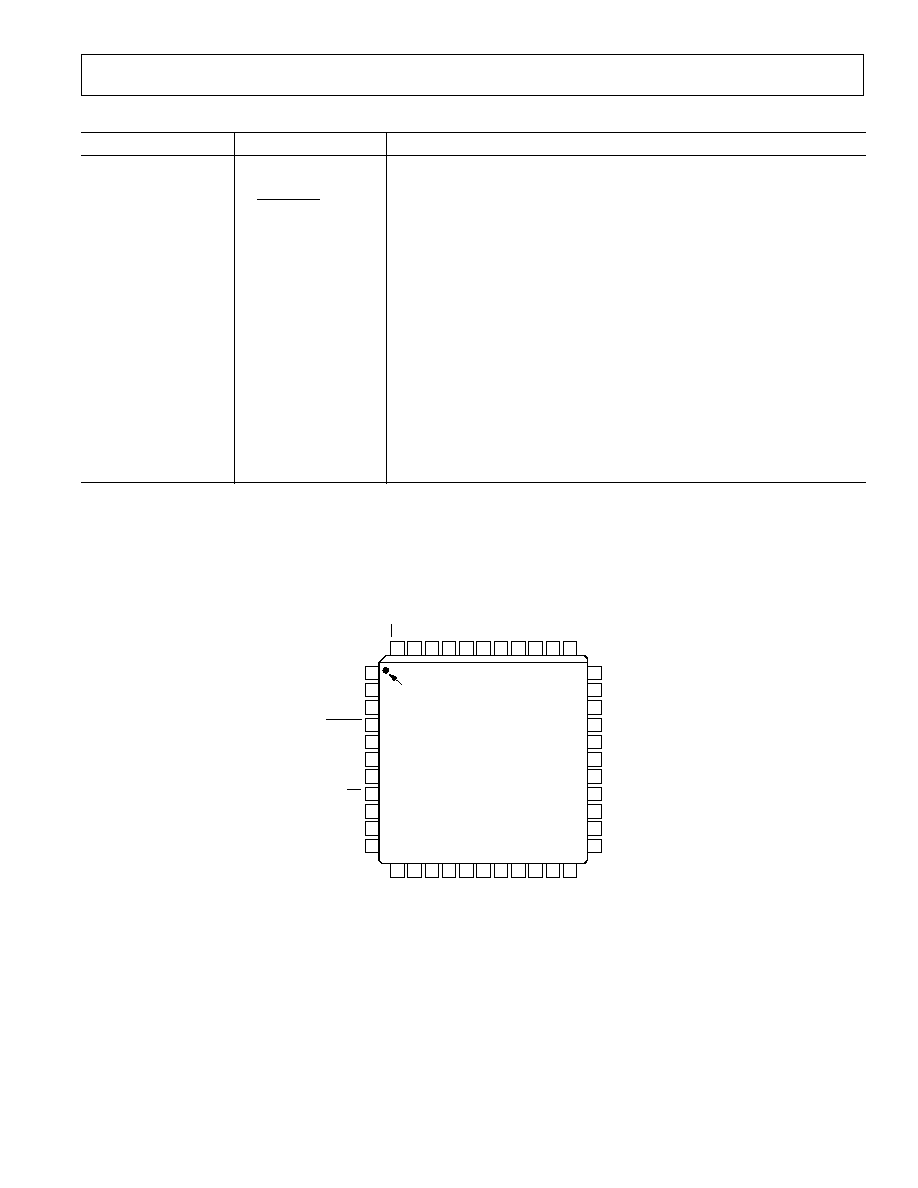
PIN FUNCTION DESCRIPTIONS
Pin No.
Name
Function
1, 2, 36, 37, 40, 41
DV
CC
+3.3 V/+5 V Power Supply (Digital). Powers output stage only.
3
ENCODE
Encode Input. Data conversion initiated on rising edge.
4
ENCODE
Complement of ENCODE. Drive differentially with ENCODE or bypass to
Ground for single-ended clock mode. See Encoding the AD6640 section.
5, 6, 13, 14, 17, 18, 21,
22, 24, 34, 35, 38, 39
GND
Ground.
7
AIN
Analog Input.
8
AIN
Complement of Analog Input.
9
V
REF
Internal Voltage Reference. Nominally +2.4 V. Bypass to Ground with
0.1
µ
F + 0.01
µ
F microwave chip capacitor.
10
C1
Internal Bias Point. Bypass to ground with 0.01
µ
F capacitor.
11, 12, 15, 16, 19, 20
AV
CC
+5 V Power Supply (Analog).
23
NC
No Connect.
25
D0 (LSB)
Digital Output Bit (Least Significant Bit).
2633
D1D8
Digital Output Bits.
42, 43
D9D10
Digital Output Bits.
44
D11 (MSB)
1
Digital Output Bit (Most Significant Bit).
NOTE
1
Output coded as twos complement.
PIN CONFIGURATION
3
4
5
6
7
1
2
10
11
8
9
40 39 38
41
42
43
44
36
35 34
37
29
30
31
32
33
27
28
25
26
23
24
12 13
14 15
16 17 18 19 20 21 22
PIN 1
TOP VIEW
(Not to Scale)
AV
CC
AV
CC
AV
CC
AV
CC
AV
CC
D8
D7
D6
D5
D4
D3
D2
AD6640
DV
CC
DV
CC
ENCODE
ENCODE
GND
GND
AIN
NC = NO CONNECT
V
REF
C1
AV
CC
D1
D0 (LSB)
GND
NC
D11 (MSB)
GND
GND
GND
GND
D10
GND
GND
GND
GND
GND
D9
DV
CC
DV
CC
DV
CC
DV
CC
GND
AIN

AD6640
6
REV. 0
DEFINITION OF SPECIFICATIONS
Analog Bandwidth (Small Signal)
The analog input frequency at which the spectral power of the
fundamental frequency (as determined by the FFT analysis) is
reduced by 3 dB.
Aperture Delay
The delay between a differential crossing of ENCODE and
ENCODE and the instant at which the analog input is sampled.
Aperture Uncertainty (Jitter)
The sample-to-sample variation in aperture delay.
Differential Nonlinearity
The deviation of any code from an ideal 1 LSB step.
Encode Pulsewidth/Duty Cycle
Pulsewidth high is the minimum amount of time that the EN-
CODE pulse should be left in logic "1" state to achieve rated
performance; pulsewidth low is the minimum time ENCODE
pulse should be left in low state. At a given clock rate, these
specs define an acceptable Encode duty cycle.
Integral Nonlinearity
The deviation of the transfer function from a reference line
measured in fractions of 1 LSB using a "best straight line"
determined by a least square curve fit.
Minimum Conversion Rate
The encode rate at which the SNR of the lowest analog signal
frequency drops by no more than 3 dB below the guaranteed
limit.
Maximum Conversion Rate
The encode rate at which parametric testing is performed.
Output Propagation Delay
The delay between a differential crossing of ENCODE and
ENCODE and the time when all output data bits are within
valid logic levels.
Power Supply Rejection Ratio
The ratio of a change in input offset voltage to a change in
power supply voltage.
Signal-to-Noise-and-Distortion (SINAD)
The ratio of the rms signal amplitude (set at 1 dB below full
scale) to the rms value of the sum of all other spectral compo-
nents, including harmonics but excluding dc.
Signal-to-Noise Ratio (SNR)
The ratio of the rms signal amplitude (set at 1 dB below full
scale) to the rms value of the sum of all other spectral compo-
nents, excluding the first five harmonics and dc.
Spurious-Free Dynamic Range (SFDR)
The ratio of the rms signal amplitude to the rms value of the
peak spurious spectral component. The peak spurious compo-
nent may or may not be a harmonic. May be reported in dBc
(i.e., degrades as signal levels is lowered), or in dBFS (always
related back to converter full scale).
Two-Tone Intermodulation Distortion Rejection
The ratio of the rms value of either input tone to the rms
value of the worst third order intermodulation product; re-
ported in dBc.
Two-Tone SFDR
The ratio of the rms value of either input tone to the rms value
of the peak spurious component. The peak spurious component
may or may not be an IMD product. May be reported in dBc
(i.e., degrades as signal levels is lowered), or in dBFS (always
related back to converter full scale).
Worst Harmonic
The ratio of the rms signal amplitude to the rms value of the
worst harmonic component, reported in dBc.
REV. 0
7
REV. 0
7
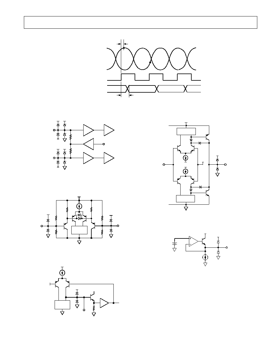
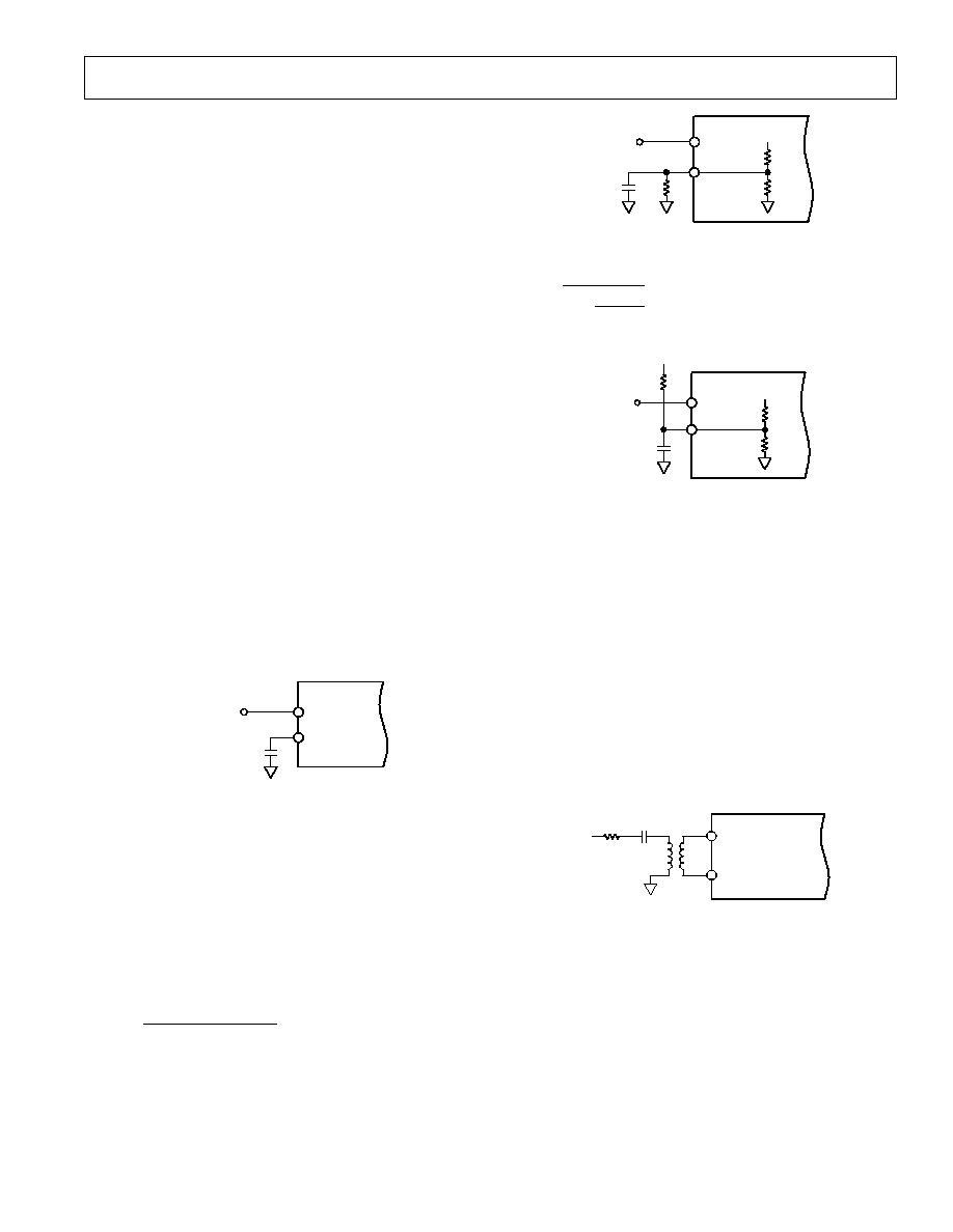
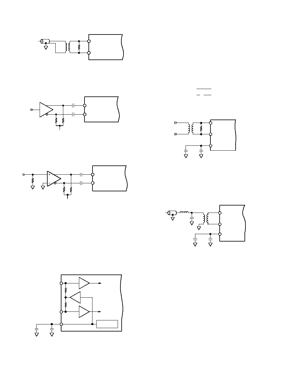
Equivalent CircuitsAD6640
450
BUF
T/H
BUF
450
BUF
T/H
AIN
AIN
V
REF
AV
CC
V
CH
AV
CC
V
CH
V
CL
V
CL
Figure 2. Analog Input Stage
AV
CC
AV
CC
TIMING
CIRCUITS
R2
8k
R2
8k
R1
17k
R1
17k
ENCODE
ENCODE
AV
CC
Figure 3. Encode Inputs
AV
CC
AV
CC
C1
CURRENT
MIRROR
V
REF
AV
CC
Figure 4. Compensation Pin, C1
V
REF
DV
CC
DV
CC
CURRENT
MIRROR
D0
D11
CURRENT
MIRROR
Figure 5. Digital Output Stage
V
REF
AV
CC
0.5mA
2.4V
AV
CC
Figure 6. 2.4 V Reference
N
DIGITAL OUTPUTS
(
D11
D0)
N 1
N 2
t
A
N + 1
t
OD
ANALOG
INPUTS
ENCODE INPUTS
(ENCODE)
N
AIN
AIN
Figure 1. Timing Diagram
AD6640
8
REV. 0
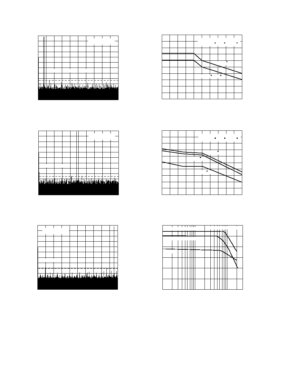
Typical Performance Characteristics
FREQUENCY MHz
0
60
100
dc
32.5
POWER RELATIVE TO ADC FULL SCALE dB
6.5
13.0
19.5
26.0
40
80
20
120
ENCODE = 65MSPS
AIN = 2.2MHz
4
8
9
5
3
7
6
2
Figure 7. Single Tone at 2.2 MHz
FREQUENCY MHz
0
60
100
dc
32.5
POWER RELATIVE TO ADC FULL SCALE dB
6.5
13.0
19.5
26.0
40
80
20
120
ENCODE = 65MSPS
AIN = 15.5MHz
4
8
9
5
3
7
6
2
Figure 8. Single Tone at 15.5 MHz
FREQUENCY MHz
0
60
100
dc
32.5
POWER RELATIVE TO ADC FULL SCALE dB
6.5
13.0
19.5
26.0
40
80
20
120
ENCODE = 65MSPS
AIN = 31.0MHz
4
8
9
5
3
7
6
2
Figure 9. Single Tone at 31.0 MHz
ANALOG INPUT FREQUENCY MHz
0
70
7
WORST CASE HARMONIC dBc
14
21
28
35
42
49
56
63
81
79
78
77
80
T = +25 C
T = 40 C, +85 C
ENCODE = 65MSPS
TEMP = 40 C, +25 C, & +85 C
Figure 10. Harmonics vs. AIN
ANALOG INPUT FREQUENCY MHz
0
70
7
SNR dB
14
21
28
35
42
49
56
63
69
67
66
65
68
ENCODE = 65MSPS
TEMP = 40 C, +25 C, & +85 C
T = +25 C
T = 40 C
T = +85 C
Figure 11. Noise vs. AIN
ENCODE = 65MSPS
ANALOG INPUT FREQUENCY MHz
90
80
30
1
100
10
SNR, HARMONICS dB, dBc
60
50
40
70
2
4
20
40
200 300
WORST OTHER SPUR
HARMONICS (2nd, 3rd)
SNR
Figure 12. Harmonics, Noise vs. AIN
AD6640
REV. 0
9
FREQUENCY MHz
0
60
100
dc
32.5
POWER RELATIVE TO ADC FULL SCALE dB
6.5
13.0
19.5
26.0
40
80
20
120
ENCODE = 65MSPS
AIN = 15.0, 16.0MHz
NO DITHER
Figure 13. Two Tones at 15.0 MHz & 16.0 MHz
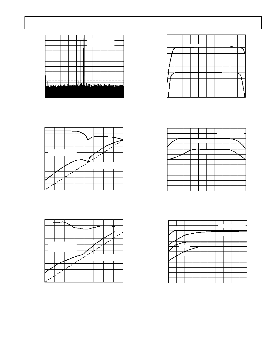
ANALOG INPUT POWER LEVEL dBFS
100
0
80
0
70
WORST CASE SPURIOUS dBc and dBFS
60
50
40
30
20
10
90
60
40
20
10
80
70
50
30
ENCODE = 65MSPS
AIN = 31.0MHz
dBFS
dBc
SFDR = 80dB
REFERENCE LINE
Figure 14. Single Tone SFDR
INPUT POWER LEVEL (F1 = F2) dBFS
100
0
80
0
70
WORST CASE SPURIOUS dBc and dBFS
60
50
40
30
20
10
90
60
40
20
10
80
70
50
30
ENCODE = 65MSPS
F1 = 15.0MHz
F2 = 16.0MHz
SFDR = 80dB
REFERENCE LINE
dBFS
dBc
Figure 15. Two Tone SFDR
SAMPLE RATE MSPS
dc
80
8
SNR, WORST CASE SPURIOUS dB, dBc
16
24
32
40
48
56
64
72
80
70
65
60
75
AIN = 19.5MHz
SNR
WORST SPUR
85
Figure 16. SNR, Worst Spurious vs. Encode
ENCODE DUTY CYCLE %
25
75
30
SNR, WORST FULL SCALE SPURIOUS dB, dBc
35
40
45
50
55
60
65
70
90
65
55
45
75
85
80
70
60
50
40
35
30
ENCODE = 65MSPS
AIN = 2.2MHz
WORST SPUR
SNR
Figure 17. SNR, Worst Spurious vs. Duty Cycle
ENCODE POWER dBm
15
15
12
SNR, WORST FULL SCALE SPURIOUS dB, dBc
9
6
3
0
3
6
9
12
90
65
55
45
75
85
80
70
60
50
40
35
30
ENCODE = 65MSPS
WORST SPUR
SNR
2.2MHz
2.2MHz
69MHz
69MHz
Figure 18. SNR, Worst Spurious vs. Encode Power
AD6640
10
REV. 0
dc
0
80
120
40
100
20
60
POWER RELATIVE TO ADC FULL SCALE dB
ENCODE = 65MSPS
AIN = 19.5MHz @ 36dBFS
NO DITHER
65
13.0
19.5
26.0
32.5
FREQUENCY MHz
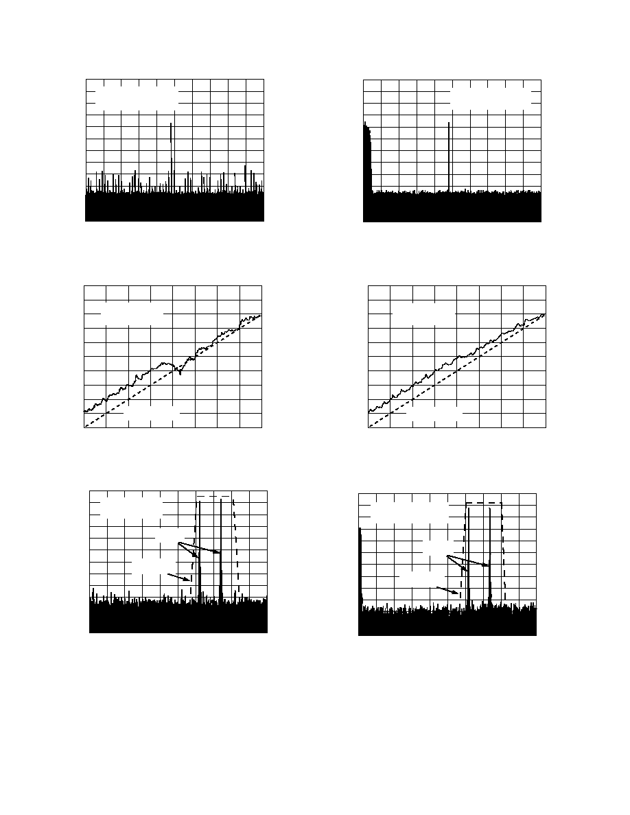
Figure 19. 16K FFT without Dither
ANALOG INPUT POWER LEVEL dBFS
100
0
80
0
70
WORST CASE SPURIOUS dBc
60
50
40
30
20
10
90
60
40
20
10
80
70
50
30
ENCODE = 65MSPS
AIN = 19.5MHz
NO DITHER
SFDR = 80dB
REFERENCE LINE
Figure 20. SFDR without Dither
50
75
55
60
65
70
FREQUENCY MHz
0
80
120
40
100
20
60
POWER RELATIVE TO ADC FULL SCALE dB
ENCODE = 50MSPS
AIN = 65.5, 68.5MHz
NO DITHER
60
90
120
30
0
ANALOG IF
FILTER MASK
ALIASED
SIGNALS
Figure 21. IF-Sampling at 70 MHz without Dither
0
80
120
40
100
20
60
POWER RELATIVE TO ADC FULL SCALE dB
ENCODE = 65MSPS
AIN = 19.5MHz @ 36dBFS
DITHER = 32.5dBm
dc
65
13.0
19.5
26.0
32.5
FREQUENCY MHz
Figure 22. 16K FFT with Dither
ANALOG INPUT POWER LEVEL dBFS
100
0
80
0
70
WORST CASE SPURIOUS dBc
60
50
40
30
20
10
90
60
40
20
10
80
70
50
30
ENCODE = 65MSPS
AIN = 19.5MHz
DITHER = 32.5dBm
SFDR = 80dB
REFERENCE LINE
Figure 23. SFDR with Dither
50
75
55
60
65
70
FREQUENCY MHz
0
80
120
40
100
20
60
POWER RELATIVE TO ADC FULL SCALE dB
ENCODE = 50MSPS
AIN = 65.5MHz, 68.5MHz
DITHER = 32.5dBm
60
90
120
30
0
ANALOG IF
FILTER MASK
ALIASED
SIGNALS
Figure 24. IF-Sampling at 70 MHz with Dither
AD6640
REV. 0
11
THEORY OF OPERATION
The AD6640 analog-to-digital converter (ADC) employs a two-
stage subrange architecture. This design approach ensures
12-bit accuracy, without the need for laser trim, at low power.
As shown in the functional block diagram, the AD6640 has
complementary analog input pins, AIN and
AIN. Each analog
input is centered at 2.4 volts and should swing
±
0.5 volts
around this reference (ref. Figure 2). Since AIN and
AIN are
180 degrees out of phase, the differential analog input signal is
2 volts peak-to-peak.
Both analog inputs are buffered prior to the first track-and-hold,
TH1. The high state of the ENCODE pulse places TH1 in
hold mode. The held value of TH1 is applied to the input of a
6-bit coarse ADC. The digital output of the coarse ADC drives
a 6-bit DAC; the DAC is 12 bits accurate. The output of the 6-
bit DAC is subtracted from the delayed analog signal at the
input of TH3 to generate a residue signal. TH2 is used as an
analog pipeline to null out the digital delay of the coarse ADC.
The 6-bit coarse ADC word and 7-bit residue word are added
together and corrected in the digital error correction logic to
generate the output word. The result is a 12-bit parallel digital
CMOS-compatible word, coded as twos complement.
APPLYING THE AD6640
Encoding the AD6640
Best performance is obtained by driving the encode pins dif-
ferentially. However, the AD6640 is also designed to interface
with TTL and CMOS logic families. The source used to drive
the ENCODE pin(s) must be clean and free from jitter. Sources
with excessive jitter will limit SNR (reference Equation 1 under
"Noise Floor and SNR").
0.01 F
TTL OR CMOS
SOURCE
ENCODE
ENCODE
AD6640
Figure 25. Single-Ended TTL /CMOS Encode
The AD6640 encode inputs are connected to a differential input
stage (see Figure 3 under EQUIVALENT CIRCUITS). With
no input signal connected to either ENCODE pin, the voltage
dividers bias the inputs to 1.6 volts. For TTL or CMOS usage,
the encode source should be connected to ENCODE, Pin 3.
ENCODE should be decoupled using a low inductance or mi-
crowave chip capacitor to ground.
If a logic threshold other than the nominal 1.6 V is required, the
following equations show how to use an external resistor, Rx, to
raise or lower the trip point (see Figure 3; R1 = 17 k
, R2 = 8 k
).
V
l
=
5R2Rx
R1R2
+
R1Rx
+
R2Rx
to lower logic threshold.
0.01 F
ENCODE
SOURCE
ENCODE
ENCODE
AD6640
RX
V
l
+5V
R1
R2
Figure 26. Lower Logic Threshold for Encode
V
l
=
5R2
R2
+
R1R
X
R1
+
R
X
to raise logic threshold.
0.01 F
ENCODE
SOURCE
ENCODE
ENCODE
AD6640
RX
V
l
+5V
R1
R2
AV
CC
Figure 27. Raise Logic Threshold for Encode
While the single-ended encode will work well for many applica-
tions, driving the encode differentially will provide increased
performance. Depending on circuit layout and system noise, a
1 dB to 3 dB improvement in SNR can be realized. It is not
recommended that differential TTL logic be used however,
because most TTL families that support complementary outputs
are not delay or slew rate matched. Instead, it is recommended
that the encode signal be ac-coupled into the ENCODE and
ENCODE pins.
The simplest option is shown below. The low jitter TTL signal
is coupled with a limiting resistor, typically 100 ohms, to the
primary side of an RF transformer (these transformers are inex-
pensive and readily available; part number in Figure 28 is from
Mini-Circuits). The secondary side is connected to the EN-
CODE and
ENCODE pins of the converter. Since both encode
inputs are self-biased, no additional components are required.
TTL
ENCODE
ENCODE
AD6640
100
T11T
0.1 F
Figure 28. TTL Source Differential Encode
A clean sine wave may be substituted for a TTL clock. In this
case, the matching network is shown below. Select a transformer
ratio to match source and load impedances. The input impedance
of the AD6640 encode is approximately 11 k
differentially.
Therefore "R," shown in the Figure 29, may be any value that is
convenient for available drive power.
AD6640
12
REV. 0
ENCODE
ENCODE
AD6640
R
T11T
SINE
SOURCE
Figure 29. Sine Source Differential Encode
If a low jitter ECL clock is available, another option is to ac-
couple a differential ECL signal to the encode input pins as
shown below. The capacitors shown here should be chip ca-
pacitors but do not need to be of the low inductance variety.
ENCODE
ENCODE
AD6640
ECL
GATE
0.1 F
0.1 F
V
S
510
510
Figure 30. Differential ECL for Encode
As a final alternative, the ECL gate may be replaced by an ECL
comparator. The input to the comparator could then be a logic
signal or a sine signal.
ENCODE
ENCODE
AD6640
0.1 F
0.1 F
V
S
50
AD96687 (1/2)
510
510
Figure 31. ECL Comparator for Encode
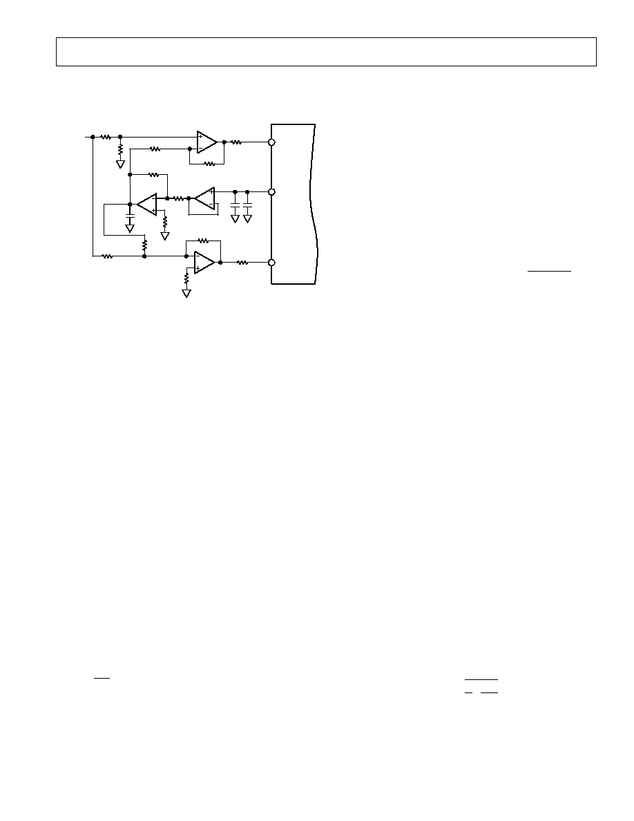
Driving the Analog Input
Because the AD6640 operates from a single +5 volt supply, the
analog input voltage range is offset from ground by 2.4 volt.
Each analog input connects through a 450 ohm resistor to the
2.4 volt bias voltage and to the input of a differential buffer
(Figure 32). This resistor network on the input properly biases
the followers for maximum linearity and range. Therefore, the
analog source driving the AD6640 should be ac-coupled to the
input pins. Since the differential input impedance of the AD6640
is 0.9 k
, the analog input power requirement is only 3 dBm,
simplifying the drive amplifier in many cases.
AD6640
450
+2.4V
REFERENCE
AIN
0.01 F
450
BUF
BUF
BUF
AIN
V
REF
0.1 F
Figure 32. Differential Analog Inputs
To take full advantage of this high input impedance, a 20:1
transformer would be required. This is a large ratio and could
result in unsatisfactory performance. In this case, a lower
step-up ratio could be used. For example, if R
T
were set to
260 ohms, along with a 4:1 transformer, the input would match
to a 50 ohm source with a full-scale drive of +4 dBm (Figure
33). Note that the external load resistor, R
T
, is in parallel with
the AD6640 analog input resistance of 900 ohms. The external
resistor value can be calculated from the following equation:
R
T
=
1
1
Z
1
900
where Z is the desired impedance (200
for a 4:1 transformer
with 50
input source).
AIN
0.01 F
AIN
V
REF
0.1 F
R
T
1:4
ANALOG
INPUT
SIGNAL
AD6640
Figure 33. Transformer-Coupled Analog Input Signal
If the lower drive power is attractive, a combination transformer
match and LC match could be employed that would use a 4:1
transformer with an LC as shown in Figure 34. This solution is
useful when good performance in the third Nyquist zone is
required. Such a requirement arises when digitizing high inter-
mediate frequencies in communications receivers.
AIN
0.01 F
AIN
V
REF
0.1 F
1:4
AD6640
j125
+j100
ANALOG
SIGNAL
AT
3dBm
Figure 34. Low Power Drive Circuit
In applications where gain is needed but dc-coupling is not
necessary, an extension of Figure 34 is recommended. A
50 ohm gain block may be placed in front of the LC matching
network. Such gain blocks are readily available for commercial
applications. These low cost modules can have excellent NF and
intermodulation performance. This circuit is especially good for
the "IF" receiver application previously mentioned.
In applications where dc-coupling is required the following
circuit can be used (Figure 35). It should be noted that the
addition of circuitry for dc-coupling may compromise performance
in terms of noise, offset and dynamic performance. This circuit
requires an inverting and noninverting signal path. Additionally,
an offset must be generated so that the analog input to each pin
is centered near 2.4 volts. Since the input is differential, small
differences in the dc voltage at each input can translate into an
offset for the circuit. The same holds true for gain mismatch.
Therefore, some means of adjusting the gain and offset between
AD6640
REV. 0
13
the device. A full-scale transition can cause up to 120 mA
(12 bits
×
10 mA/bit) of current to flow through the digital
output stages. The series resistor will minimize the output
currents that can flow in the output stage. These switching
currents are confined between ground and the DV
CC
pin. Stan-
dard TTL gates should be avoided since they can appreciably
add to the dynamic switching currents of the AD6640.
Layout Information
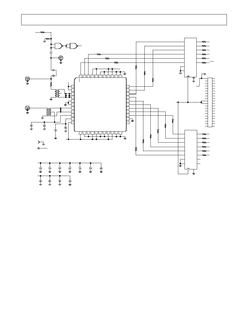
The schematic of the evaluation board (Figure 36) represents a
typical implementation of the AD6640. The pinout of the
AD6640 facilitates ease of use and the implementation of high
frequency/high resolution design practices. All of the digital
outputs are on one side while the other sides contain all of the
inputs. It is highly recommended that high quality ceramic chip
capacitors be used to decouple each supply pin to ground di-
rectly at the device. Depending on the configuration used for
the encode and analog inputs, one or more capacitors are required
on those input pins. The capacitors used on the
ENCODE and
V
REF
pins must be a low inductance chip capacitor as referenced
previously in the data sheet.
A multilayer board is recommended to achieve best results. Care
should be taken when placing the digital output runs. Because
the digital outputs have such a high slew rate, the capacitive
loading on the digital outputs should be minimized. Circuit
traces for the digital outputs should be kept short and connect
directly to the receiving gate (broken only by the insertion of the
series resistor). Digital data lines should be kept clear of analog
and encode traces.
Evaluation Boards
The evaluation board for the AD6640 is very straightforward,
consisting of power, signal inputs and digital outputs. The
evaluation board includes the option for an onboard clock oscil-
lator for the encode.
Power to the analog supply pins is connected via banana jacks.
The analog supply powers the crystal oscillator and the AV
CC
pins of the AD6640.
The DV
CC
power is supplied via J3, the digital interface. This
digital supply connection also powers the digital gates on the
PCB. By maintaining separate analog and digital power supplies,
degradation in SNR and SFDR is kept to a minimum. Total
power requirement is approximately 200 mA. This configuration
allows for easy evaluation of different logic families (i.e., con-
nection to a 3.3 volt logic board).
The analog input is connected via J2 and is transformer-coupled
to the AD6640 (see Driving the Analog Input). The onboard
termination resistor is 270
. This resistor, in parallel with the
AD6640's input resistance (900
), provides a 50
load to the
analog source driving the 1:4 transformer. If a different input
impedance is required, replace R16 by using the following
equation
R16
=
1
1
Z
-
1
900
where Z is desired input impedance (200
for a 4:1 trans-
former with 50
source).
the sides should be implemented. The addition of small value
resistors between the AD9631 and the AD6640 will prevent
oscillation due to the capacitive input of the ADC.
62
SIGNAL
SOURCE
AD9631
15
467
0.1 F
OP279
(1/2)
OP279
(1/2)
750
1000
78
350
AD6640
AIN
V
REF
425
467
0.1 F
0.01 F
127
350
AD9631
15
AIN
350
Figure 35. DC-Coupled Analog Input Circuit
Power Supplies
Care should be taken when selecting a power source. Linear
supplies are strongly recommended as switching supplies tend to
have radiated components that may be "received" by the
AD6640. Each of the power supply pins should be decoupled as
closely to the package as possible using 0.1
µ
F chip capacitors.
The AD6640 has separate digital and analog +5 V pins. The
analog supplies are denoted AV
CC
and the digital supply pins
are denoted DV
CC
. Although analog and digital supplies may be
tied together, best performance is achieved when the supplies
are separate. This is because the fast digital output swings can
couple switching noise back into the analog supplies. Note that
AV
CC
must be held within 5% of 5 volts; however the DV
CC
supply may be varied according to output digital logic family
(i.e., DV
CC
should be connected to the same supply as the digi-
tal circuitry). The AD6640 is specified for DV
CC
= 3.3 V as this
is a common supply for digital ASICs.
Output Loading
Care must be taken when designing the data receivers for the
AD6640. It is recommended that the digital outputs drive a
series resistor (e.g. 348 ohms) followed by a gate like the
74LCX574. To minimize capacitive loading, there should only
be one gate on each output pin. An example of this is shown in
the evaluation board schematic shown in Figure 36. The digital
outputs of the AD6640 have a constant rise time output stage.
The output slew rate is about 1 V/ns when DV
CC
= +5 V. A
typical CMOS gate combined with PCB trace and through hole
will have a load of approximately 10 pF. Therefore as each bit
switches, 10 mA
10 pF
×
1V
1ns
of dynamic current per bit will flow in or out of

AD6640
14
REV. 0
The analog input range of the PCB is
±
0.5 volts (i.e., signal ac-
coupled to AD6640).
The encode signal may be generated using an onboard crystal
oscillator, U1. The oscillator is socketed and may be replaced
by an external encode source via J1. If an external source is
used, it should be a high quality TTL source. A transformer
converts the single-ended TTL signal to a differential clock (see
Encoding the AD6640). Since the encode is coupled with a
transformer, a sine wave could have been used; note, however,
that U5 requires TTL levels to function properly.
Table I. AD6640ST/PCB Bill of Material
Item
Quantity
Reference
Description
1
2
+5 VA, GND
Banana Jack
2
11
C7C9, C11C17, C19
Ceramic Chip Capacitor 0805, 0.1
µ
F
3
2
C4, C6
Tantalum Chip Capacitor 10
µ
F
4
1
J3
40-Pin Double Row Male Header
5
3
J1, J2, J4
BNC Coaxial PCB Connector
6
1
R1
Surface Mount Resistor 1206, 348
7
25
R2R14, R20R25, R30R35
Surface Mount Resistor 1206, 348
8
1
R15
Surface Mount Resistor 1206, 100
9
1
R16
Surface Mount Resistor 1206, 270
10
2
T1, T2
Surface Mount Transformer Mini-Circuits T41T, 1:4 Ratio
11
1
U1
Clock Oscillator (Optional)
12
1
DUT
AD6640AST 12-Bit65 MSPS ADC Converter
13
2
U3, U4
74LCX574 Octal Latch
14
1
U5
74LVQ00 Quad Two Input NAND Gate
15
1
C1, C18
Ceramic Chip Capacitor 0508, 0.01
µ
F Low Inductance
16
2
C2, C3
Ceramic Chip Capacitor 0508, 0.1
µ
F Low Inductance
17
2
CR1, CR2
1N2810 Schottky Diode
AD6640 output data is latched using 74LCX574 (U3, U4)
latches following 348 ohm series resistors. The resistors limit
the current that would otherwise flow due to the digital output
slew rate. The resistor value was chosen to represent a time
constant of ~25% of the data rate at 65 MHz. This reduces slew
rate while not appreciably distorting the data waveform. Data is
latched in a pipeline configuration; a rising edge generates the
new AD6640 data sample, latches the previous data at the con-
verter output, and strobes the external data register over J3.
NOTE: Power and ground must be applied to J3 to power the
digital logic section of the evaluation board.
AD6640
REV. 0
15
29
30
31
32
33
27
28
25
26
24
23
3
4
5
6
7
2
10
11
8
9
1
40
39
38
41
42
43
44
36
35
34
37
12
13
14
15
16
17
18
19
20
21
22
2
9
8
7
6
3
4
5
12
13
14
15
16
17
18
19
74LCX574
(DV
CC
)
8D
7D
5D
1D
4D
6D
3D
2D
5Q
6Q
7Q
8Q
2Q
3Q
4Q
1Q
OE
CK
B06
B07
B08
B09
B10
B11
11
1
2
9
8
7
6
3
4
5
12
13
14
15
16
17
18
19
U4
74LCX574
(DV
CC
)
8D
7D
5D
1D
4D
6D
3D
2D
5Q
6Q
7Q
8Q
2Q
3Q
4Q
1Q
OE
CK
B00
B01
B02
B03
B04
B05
11
1
NC = NO CONNECT
GND
GND
GND
DV
CC
DV
CC
3
2
1
4
6
T41T
100
1
2
3
U5
74LVQ00
(+5VA)
5
6
4
BUFLAT
ANALOG
INPUT
+5V ANALOG
SUPPLY
+5VA
GND
COMMON
0.1 F
1:4
0.01 F
GND
GND
GND
GND
DV
CC
C6
10 F
+
C7
0.1 F
C11
0.1 F
C12
0.1 F
C13
0.1 F
C15
0.1 F
C16
0.1 F
+5VA
C4
10 F
+
C8
0.1 F
C9
0.1 F
C17
0.1 F
AV
CC
AV
CC
AV
CC
AV
CC
AV
CC
DUT
AD6640
DV
CC
ENCODE
ENCODE
AIN
V
REF
C1
AV
CC
GND
GND
GND
GND
D10
D9
DV
CC
DV
CC
DV
CC
DV
CC
GND
348
348
348
348
348
348
348
348
348
348
348
348
0.01 F
D8
D7
D6
D5
D4
D3
D2
D1
GND
NC
(LSB) D0
D11
DV
CC
+5VA
3
2
1
4
6
T41T
1:4
TWO COMPLEMENT
BUFFERED OUTPUTS
E1
E2
270
0.1 F
+5VA
348
J1
J2
ENCODE
INPUT
0.1 F
1
2
3
4
5
6
7
8
9
10
11
12
13
14
15
16
17
18
19
20
31
30
29
28
27
26
25
24
23
22
21
32
33
34
35
36
37
38
39
40
GND
GND
GND
GND
GND
GND
GND
GND
GND
GND
GND
GND
GND
GND
GND
GND
GND
GND
GND
GND
DV
CC
(+3.3V OR +5.0V)
B11
B10
B09
B08
B07
B06
B05
B04
B03
B02
B01
B00
GND
GND
GND
GND
GND
348
348
348
348
348
348
348
348
348
348
348
348
BUFLAT
348
AIN
J4
J3
DV
CC
Figure 36. AD6640ST/PCB Schematic
AD6640
16
REV. 0
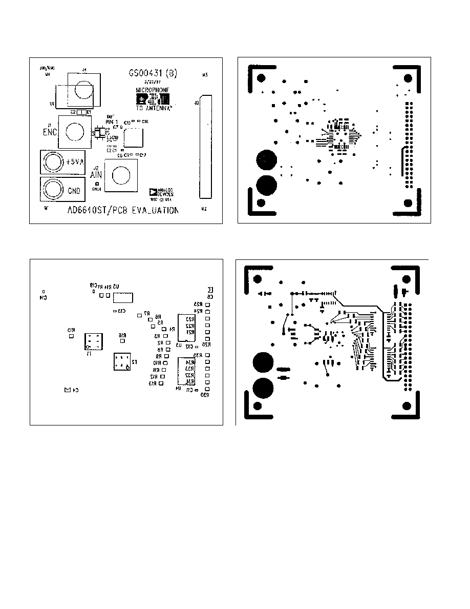
Figure 37. AD6640ST/PCB Top Side Silkscreen
Figure 38. AD6640ST/PCB Bottom Side Silkscreen
Figure 39. AD6640ST/PCB Top Side Copper
Figure 40. AD6640ST/PCB Bottom Side Copper (Positive)
NOTE: Evaluation boards are often updated, consult factory for latest version.
AD6640
REV. 0
17
Figure 41. AD6640ST/PCB Ground Layer (Negative)
Figure 42. AD6640ST/PCB "Split" Power Layer (Negative)
AD6640
18
REV. 0
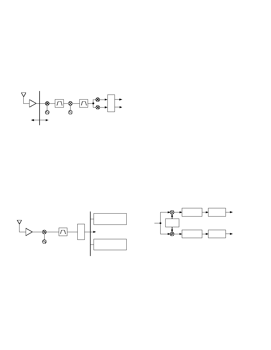
DIGITAL WIDEBAND RECEIVERS
Introduction
Several key technologies are now being introduced that may
forever alter the vision of radio. Figure 43 shows the typical
dual conversion superheterodyne receiver. The signal picked up
by the antenna is mixed down to an intermediate frequency (IF)
using a mixer with a variable local oscillator (LO); the variable
LO is used to "tune-in" the desired signal. This first IF is
mixed down to a second IF using another mixer stage and a
fixed LO. Demodulation takes place at the second or third IF
using either analog or digital techniques.
ADCs
VARIABLE
IF
1
IF
2
FIXED
NARROWBAND
FILTER
NARROWBAND
FILTER
I
Q
LNA
RF
e.g. 900MHz
SHARED
ONE RECEIVER PER CHANNEL
Figure 43. Narrowband Digital Receiver Architecture
If demodulation takes place in the analog domain then tradi-
tional discriminators, envelop detectors, phase locked loops or
other synchronous detectors are generally employed to strip the
modulation from the selected carrier.
However, as general purpose DSP chips such as the ADSP-2181
become more popular, they will be used in many baseband-
sampled applications like the one shown in Figure 43. As
shown in the figure, prior to ADC conversion, the signal must
be mixed down, filtered, and the I and Q components separated.
These functions are realizable through DSP techniques, how-
ever several key technology breakthroughs are required: high
dynamic range ADCs such as the AD6640, new DSPs (highly
programmable with onboard memory, fast), digital tuners and
filters such as the AD6620, wide band mixers and amplifiers.
WIDEBAND
ADC
FIXED
WIDEBAND
MIXER
WIDEBAND
FILTER
LNA
RF
e.g. 900MHz
SHARED
"n" CHANNELS
TO DSP
12.5MHz
(416 CHANNELS)
CHANNEL SELECTION
DIGITAL TUNER/FILTER
DSP
DIGITAL TUNER/FILTER
DSP
Figure 44. Wideband Digital Receiver Architecture
Figure 44 shows such a wideband system. This design shows
that the front end variable local oscillator has been replaced with
a fixed oscillator and the back end has been replaced with a
wide dynamic range ADC, digital tuner and DSP. This tech-
nique offers many benefits.
First, many passive discrete components have been eliminated
that formed the tuning and filtering functions. These passive
components often require "tweaking" and special handling
during assembly and final system alignment. Digital compo-
nents require no such adjustments; tuner and filter characteristics
are always exactly the same. Moreover, the tuning and filtering
characteristics can be changed through software. Since software
is used for demodulation, different routines may be used to
demodulate different standards such as AM, FM, GMSK or any
other desired standard. In addition, as new standards arise or
new software revisions are generated, they may be field installed
with standard software update channels. A radio that performs
demodulation in software as opposed to hardware is often
referred to as a soft radio because it may be changed or modified
simply through code revision.
System Description
In the wideband digital radio (Figure 44), the first down conver-
sion functions in much the same way as a block converter does.
An entire band is shifted in frequency to the desired interme-
diate frequency. In the case of cellular base station receivers,
5 MHz to 30 MHz of bandwidth are down-converted simulta-
neously to an IF frequency suitable for digitizing with a wide-
band analog-to-digital converter. Once digitized the broadband
digital data stream contains all of the in-band signals. The
remainder of the radio is constructed digitally using special
purpose and general purpose programmable DSP to perform
filtering, demodulation and signal conditioning not unlike the
analog counter parts.
In the narrowband receiver (Figure 43), the signal to be received
must be tuned. This is accomplished by using a variable local
oscillator at the first mix down stage. The first IF then uses a
narrow band filter to reject out of band signals and condition
the selected carrier for signal demodulation.
In the digital wideband receiver (Figure 44), the variable local
oscillator has been replaced with a fixed oscillator, so tuning
must be accomplished in another manner. Tuning is performed
digitally using a digital down conversion and filter chip fre-
quently called a channelizer. The term channelizer is used
because the purpose of these chips is to select one channel out
of many within the broadband spectrum present in the digital
data stream of the ADC.
DECIMATION
FILTER
LOW-PASS
FILTER
DIGITAL
TUNER
COS
SIN
DECIMATION
FILTER
LOW-PASS
FILTER
DATA
I
Q
Figure 45. AD6620 Digital Channelizer
Figure 45 shows the block diagram of a typical channelizer, such
as the AD6620. Channelizers consist of a complex NCO (Nu-
merically Controlled Oscillator), dual multiplier (mixer), and
matched digital filters. These are the same functions that would
be required in an analog receiver, however implemented in
digital form. The digital output from the channelizer is the
desired carrier, frequently in I & Q format; all other signals have
been filtered and removed based on the filtering characteristics
desired. Since the channelizer output consists of one selected
RF channel, one tuner chip is required for each frequency re-
ceived, although only one wideband RF receiver is needed for
the entire band. Data from the channelizer may then be pro-
cessed using a digital signal processor such as the ADSP-2181
or the SHARC
®
processor, the ADSP-21062. This data may
then be processed through software to demodulate the informa-
tion from the carrier.
SHARC is a registered trademark of Analog Devices, Inc.
AD6640
REV. 0
19
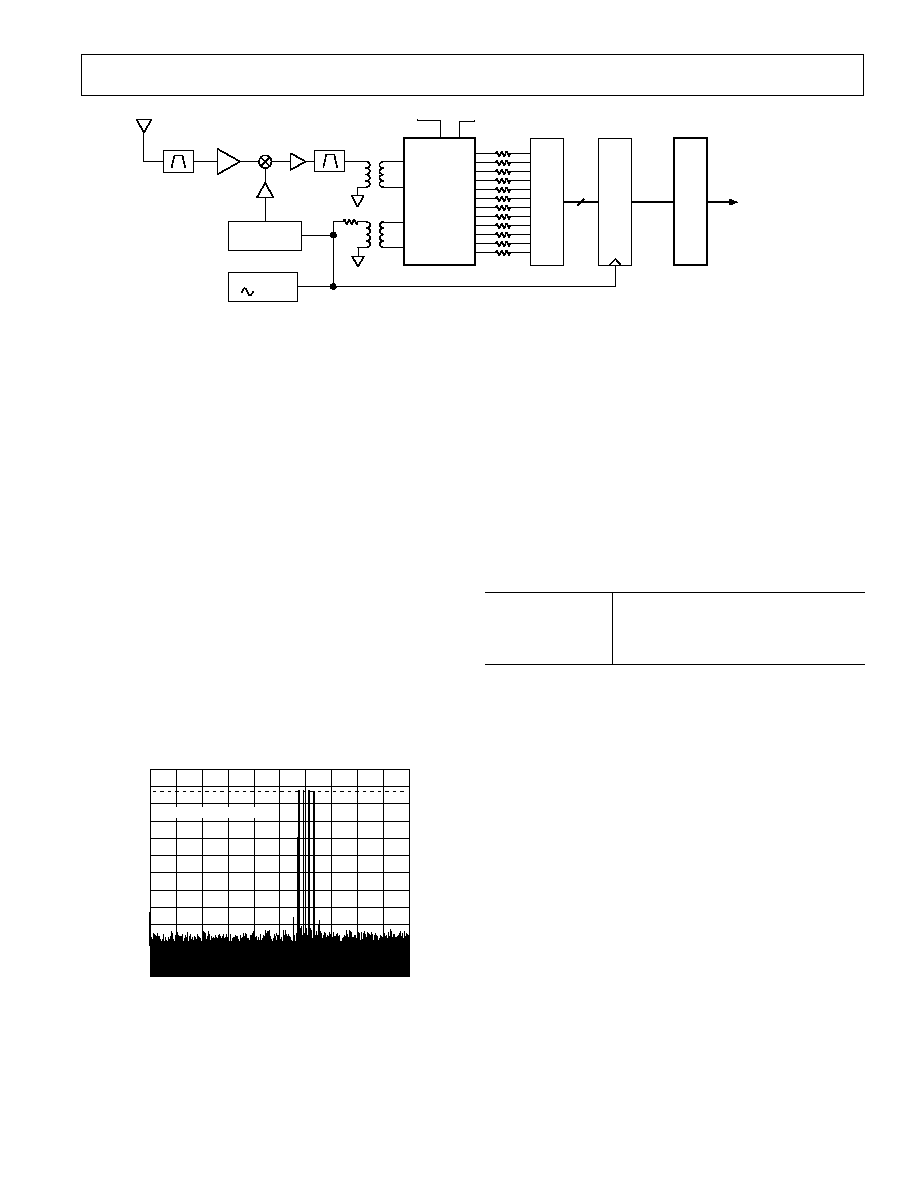
System Requirements
Figure 46 shows a typical wideband receiver subsystem based
around the AD6640. This strip consists of a wideband IF filter,
amplifier, ADC, latches, channelizer and interface to a digital
signal processor. This design shows a typical clocking scheme
used in many receiver designs. All timing within the system is
referenced back to a single clock. While this is not necessary, it
does facilitate PLL design, ease of manufacturing, system test,
and calibration. Keeping in mind that the overall performance
goal is to maintain the best possible dynamic range, many con-
siderations must be made.
One of the biggest challenges is selecting the amplifier used to
drive the AD6640. Since this is a communications application,
it is common to directly sample an intermediate frequency (IF)
signal. As such, IF gain blocks can be implemented instead of
baseband op amps. For these gain block amplifiers, the critical
specifications are third order intercept point and noise figure. A
bandpass filter will remove harmonics generated within the
amplifier, but intermods should be better than the performance
of the A/D converter. In the case of the AD6640, amplifier
intermods must be better than 80 dBFS when driving full-
scale power. As mentioned earlier, there are several amplifiers
to choose from and the specifications depend on the end
application. Figure 47 shows a typical multitone test.
FREQUENCY MHz
0
80
120
40
100
20
60
dc
32.5
6.5
POWER RELATIVE TO ADC FULL SCALE dB
13.0
19.5
26.0
ENCODE = 65MSPS
Figure 47. Multitone Performance
Two other key considerations for the digital wideband receiver
are converter sample rate and IF frequency range. Since per-
formance of the AD6640 converter is largely independent of
both sample rate and analog input frequency (Figures 10, 11
and 16), the designer has greater flexibility in the selection of
these parameters. Also, since the AD6640 is a bipolar device,
power dissipation is not a function of sample rate. Thus there is
no penalty paid in power by operating at faster sample rates. All
of this is good because, by carefully selecting input frequency
range and sample rate, some of the drive amplifier and ADC
harmonics can actually be placed out-of-band.
For example, if the system has second and third harmonics that
are unacceptably high, by carefully selecting the encode rate and
signal bandwidth, these second and third harmonics can be
placed out-of-band. For the case of an encode rate equal to
60 MSPS and a signal bandwidth of 7.5 MHz, placing the fun-
damental at 7.5 MHz places the second and third harmonics out
of band as shown in the table below.
Table II.
Encode Rate
60 MSPS
Fundamental
7.5 MHz15 MHz
Second Harmonic
15 MHz30 MHz
Third Harmonic
22.5 MHz30 MHz, 30 MHz15 MHz
Another option can be found through bandpass sampling. If the
analog input signal range is from dc to FS/2, then the amplifier
and filter combination must perform to the specification re-
quired. However, if the signal is placed in the third Nyquist
zone (FS to 3 FS/2), the amplifier is no longer required to meet
the harmonic performance required by the system specifications
since all harmonics would fall outside the passband filter. For
example, the passband filter would range from FS to 3 FS/2.
The second harmonic would span from 2 FS to 3 FS, well out-
side the passband filter's range. The burden then has been passed
off to the filter design provided that the ADC meets the basic
specifications at the frequency of interest. In many applications,
this is a worthwhile tradeoff since many complex filters can
easily be realized using SAW and LCR techniques alike at these
relatively high IF frequencies. Although harmonic performance
of the drive amplifier is relaxed by this technique, intermodula-
tion performance cannot be sacrificed since intermods must be
assumed to fall in-band for both amplifiers and converters.
Noise Floor and SNR
Oversampling is sampling at a rate that is greater than twice the
bandwidth of the signal desired. Oversampling does not have
anything to do with the actual frequency of the sampled sig-
nal, it is the bandwidth of the signal that is key. Bandpass or
"IF" sampling refers to sampling a frequency that is higher than
Nyquist and often provides additional benefits such as down
conversion using the ADC and replacing a mixer with a track-
and-hold. Oversampling leads to processing gains because the
PRESELECT
FILTER
LNA
515MHz
PASSBAND
348
CMOS
BUFFER
D11
D0
+3.3V (D)
+5V (A)
AD6640
AIN
ENCODE
ENCODE
M/N PLL
SYNTHESIZER
LO
DRIVE
REF
IN
1900MHz
REFERENCE
CLOCK
65.00MHz
12
AD6620
(REF. FIG 45)
I & Q
DATA
CLK
ADSP-2181
NETWORK
CONTROLLER
INTERFACE
AIN
Figure 46. Simplified Wideband PCS Receiver
AD6640
20
REV. 0
faster the signal is digitized, the wider the distribution of noise.
Since the integrated noise must remain constant, the actual
noise floor is lowered by 3 dB each time the sample rate is
doubled. The effective noise density for an ADC may be calcu-
lated by the equation:
V
NOISE rms
/
Hz
=
10
-
SNR /20
4 FS
For a typical SNR of 68 dB and a sample rate of 65 MSPS, this
is equivalent to 25 nV/
Hz. This equation shows the relation-
ship between SNR of the converter and the sample rate FS.
This equation may be used for computational purposes to deter-
mine overall receiver noise.
The signal-to-noise ratio (SNR) for an ADC can be predicted.
When normalized to ADC codes, the following equation accu-
rately predicts the SNR based on three terms. These are jitter,
average DNL error and thermal noise. Each of these terms
contributes to the noise within the converter.
Equation 1:
SNR
=
20 log
2
FANALOG tJ rms
(
)
2
+
1
+
2
12
2
+
VNOISE rms
2
12
2
1/2
F
ANALOG
= analog input frequency
t
J rms
= rms jitter of the encode (rms sum of encode source
and internal encode circuitry)
= average DNL of the ADC (typically 0.51 LSB)
V
NOISE rms
= V rms thermal noise referred to the analog input of
the ADC (typically 0.707 LSB)
Processing Gain
Processing gain is the improvement in signal-to-noise ratio
(SNR) gained through oversampling and digital filtering. Most
of this processing gain is accomplished using the channelizer
chips. These special purpose DSP chips not only provide chan-
nel selection and filtering but also provide a data rate reduction.
The required rate reduction is accomplished through a process
called decimation. The term decimation rate is used to indicate
the ratio of input data rate to output data rate. For example, if
the input data rate is 65 MSPS and the output data rate is
1.25 MSPS, then the decimation rate is 52.
Large processing gains may be achieved in the decimation and
filtering process. The purpose of the channelizer, beyond tun-
ing, is to provide the narrowband filtering and selectivity that
traditionally has been provided by the ceramic or crystal filters
of a narrowband receiver. This narrowband filtering is the
source of the processing gain associated with a wideband re-
ceiver and is simply the ratio of the passband to whole band
expressed in dB. For example, if a 30 kHz AMPS signal is
being digitized with an AD6640 sampling at 65 MSPS, the ratio
would be 0.015 MHz/32.5 MHz. Expressed in log form, the
processing gain is 10
×
log (0.015 MHz/32.5 MHz) or 33.4 dB.
Additional filtering and noise reduction techniques can be
achieved through DSP techniques; many applications do use
additional process gains through proprietary noise reduction
algorithms.
Overcoming Static Nonlinearities with Dither
Typically, high resolution data converters use multistage
techniques to achieve high bit resolution without large com-
parator arrays that would be required if traditional "flash" ADC
techniques were employed. The multistage converter typically
provides better wafer yields meaning lower cost and much lower
power. However, since it is a multistage device, certain portions
of the circuit are used repetitively as the analog input sweeps
from one end of the converter range to the other. Although the
worst DNL error may be less than an LSB, the repetitive nature
of the transfer function can play havoc with low level dynamic
signals. Spurious signals for a full-scale input may be 80 dBc.
However at 36 dB below full scale, these repetitive DNL errors
may cause spurious-free dynamic range (SFDR) to fall below
80 dBFS as shown in Figure 20.
A common technique for randomizing and reducing the effects
of repetitive static linearity is through the use of dither. The
purpose of dither is to force the repetitive nature of static linear-
ity to appear as if it were random. Then, the average linearity
over the range of dither will dominate SFDR performance. In
the AD6640, the repetitive cycle is every 15.625 mV p-p.
To ensure adequate randomization, 5.3 mV rms is required;
this equates to a total dither power of 32.5 dBm. This will
randomize the DNL errors over the complete range of the
residue converter. Although lower levels of dither such as that
from previous analog stages will reduce some of the linearity
errors, the full effect will only be gained with this larger dither.
Increasing dither even more may be used to reduce some of the
global INL errors. However, signals much larger than the mVs
proposed here begin to reduce the usable dynamic range of the
converter.
Even with the 5.3 mV rms of noise suggested, SNR would be
limited to 36 dB if injected as broadband noise. To avoid this
problem, noise may be injected as an out-of-band signal. Typically,
this may be around dc but may just as well be at FS/2 or at
some other frequency not used by the receiver. The bandwidth
of the noise is several hundred kilohertz. By band-limiting and
controlling its location in frequency, large levels of dither may
be introduced into the receiver without seriously disrupting
receiver performance. The result can be a marked improvement
in the SFDR of the data converter.
Figure 23 shows the same converter shown earlier but with this
injection of dither (reference Figure 20).
AD600
A
A
REF
2.2k
1 F
0.1 F
39
390
16k
+15V
NC202
NOISE
DIODE
(NoiseCom)
+5V
5V
1k
2k
OP27
OPTIONAL HIGH
POWER DRIVE
CIRCUIT
LOW CONTROL
(01 VOLT)
Figure 48. Noise Source (Dither Generator)
AD6640
REV. 0
21
The simplest method for generating dither is through the use of
a noise diode (Figure 48). In this circuit, the noise diode NC202
generates the reference noise that is gained up and driven by the
AD600 and OP27 amplifier chain. The level of noise may be
controlled by either presetting the control voltage when the
system is set up, or by using a digital-to-analog converter (DAC)
to adjust the noise level based on input signal conditions. Once
generated, the signal must be introduced to the receiver strip.
The easiest method is to inject the signal into the drive chain
after the last down conversion as shown in Figure 49.
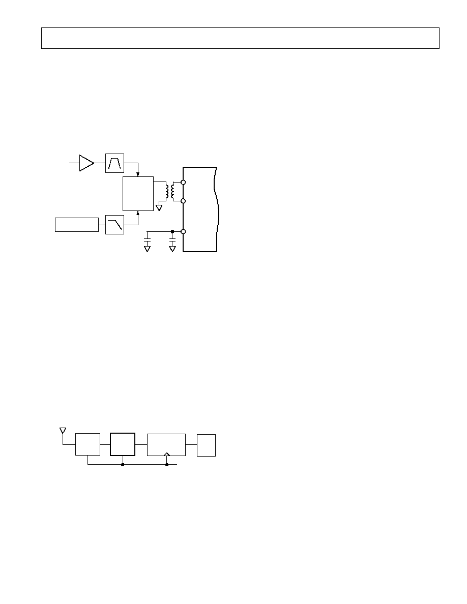
NOISE SOURCE
(REF. FIGURE 48)
LPF
AIN
0.01 F
AIN
V
REF
0.1 F
AD6640
COMBINER
BPF
FROM
RF/IF
IF AMP
Figure 49. Using the AD6640 with Dither
Receiver Example
To determine how the ADC performance relates to overall re-
ceiver sensitivity, the simple receiver in Figure 50 will be exam-
ined. This example assumes that the overall down conversion
process can be grouped into one set of specifications, instead of
individually examining all components within the system and
summing them together. Although a more detailed analysis
should be employed in a real design, this model will provide a
good approximation.
In examining a wideband digital receiver, several considerations
must be applied. Although other specifications are important,
receiver sensitivity determines the absolute limits of a radio
excluding the effects of other outside influences. Assuming that
receiver sensitivity is limited by noise and not adjacent signal
strength, several sources of noise can be identified and their
overall contribution to receiver sensitivity calculated.
RF/IF
AD6640
CHANNELIZER
REF IN
DSP
ENC
61.44MHz
GAIN = 30dB
NF = 10dB
BW =12.5MHz
SINGLE CHANNEL
BW = 30kHz
Figure 50. Receiver Analysis
The first noise calculation to make is based on the signal band-
width at the antenna. In a typical broadband cellular receiver,
the IF bandwidth is 12.5 MHz. Given that the power of noise in
a given bandwidth is defined by P
n
= kTB, where B is band-
width, k = 1.38
×
10
23
is Boltzman's constant and T = 300k
is absolute temperature, this gives an input noise power of
5.18
×
10
14
watts or 102.86 dBm. If our receiver front end has
a gain of 30 dB and a noise figure of 10 dB, then the total noise
presented to the ADC input becomes 62.86 dBm (102.86 + 30
+ 10) or 0.16 mV rms. Comparing receiver noise to dither re-
quired for good SFDR, we see that in this example, our receiver
supplies about 3% of the dither required for good SFDR.
Based on a typical ADC SNR specification of 68 dB, the
equivalent internal converter noise is 0.140 mV rms. There-
fore total broadband noise is 0.21 mV rms. Before process-
ing gain, this is an equivalent SNR (with respect to full scale)
of 64.5 dB. Assuming a 30 kHz AMPS signal and a sample
rate of 61.44 MSPS, the SNR through processing gain is in-
creased by approximately 33 dB to 97.5 dB. However, if eight
strong and equal signals are present in the ADC bandwidth,
then each must be placed 18 dB below full scale to prevent
ADC overdrive. Therefore we give away 18 dB of range and
reduce the carrier-to-noise ratio (C/N) to 79.5 dB.
Assuming that the C/N ratio must be 10 dB or better for
accurate demodulation, one of the eight signals may be reduced by
66.5 dB before demodulation becomes unreliable. At this point,
the input signal power would be 90.5 dBm. Referenced to the
antenna, this is 120.5 dBm.
To improve sensitivity, several things can be done. First, the
noise figure of the receiver can be reduced. Since front end
noise dominates the 0.16 mV rms, each dB reduction in noise
figure translates to an additional dB of sensitivity. Second, pro-
viding broadband AGC can improve sensitivity by the range of
the AGC. However, the AGC would only provide useful im-
provements if all in-band signals are kept to an absolute minimal
power level so that AGC can be kept near the maximum gain.
This noise limited example does not adequately demonstrate the
true limitations in a wideband receiver. Other limitations such
as SFDR are more restrictive than SNR and noise. Assume that
the analog-to-digital converter has an SFDR specification of
80 dBFS or 76 dBm (Full scale = +4 dBm). Also assume
that a tolerable carrier-to-interferer (C/I) (different from C/N)
ratio is 18 dB. This means that the minimum signal level is
62 dBFS (80 plus 18) or 58 dBm. At the antenna, this is
88 dBm. Therefore, as can be seen, SFDR (single or multi-
tone) would limit receiver performance in this example. How-
ever, as shown previously, SFDR can be greatly improved
through the use of dither (Figures 19, 22). In many cases, the
addition of the out-of-band dither can improve receiver sensitiv-
ity nearly to that limited by thermal noise.
AD6640
22
REV. 0
IF Sampling, Using the AD6640 as a Mix-Down Stage
Since performance of the AD6640 extends beyond the baseband
region into the third Nyquist zone, the converter has many uses
as a mix-down converter in both narrowband and wideband
applications. This application is called bandpass sampling. Do-
ing this has several positive implications in terms of the selection
of the IF drive amplifier. Not only is filtering a bit easier, the
selection of drive amplifiers is extended to classical IF gain
blocks. In the third Nyquist zone and above, the second and
third harmonics are easily filtered with a bandpass filter. Now
only in-band spurs that result from third order products are
important.
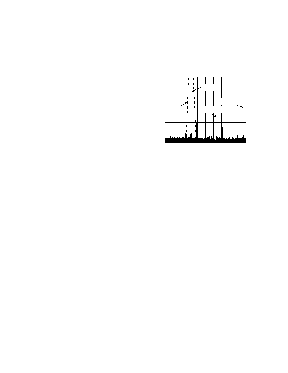
In narrowband applications, harmonics of the ADC can be
placed out-of-band. One example is the digitization of a
201 MHz IF signal using a 17.333 MHz clock. As shown in
Figure 51, the spurious performance has diminished due to
internal slew rate limitations of the ADC. However, the SNR of
the converter is still quite good. Subsequent digital filtering with
a channelizer chip such as the AD6620 will yield even better SNR.
For multicarrier applications, third order intercept of the drive
amplifier is important. If the input network is matched to the
internal 900 ohm input impedance, the required full-scale drive
level is 3 dBm. If spurious products delivered to the ADC are
required to be below 90 dBFS, the typical performance of the
ADC with dither applied, then the required third order intercept
point for the drive amplifier can be calculated.
For multicarrier applications, the AD6640 is useful up to about
80 MHz analog in. For single channel applications, the AD6640
is useful to 200 MHz as shown from the bandwidth charts. In
either case, many common IF frequencies exist in this range of
frequencies. If the ADC is used to sample these signals, they will
be aliased down to baseband during the sampling process in
much the same manner that a mixer will down-convert a signal.
For signals in various Nyquist zones, the following equations
may be used to determine the final frequency after aliasing.
f
1NYQUISTS
=
f
SAMPLE
-
f
SIGNAL
f
2NYQUISTS
=
abs ( f
SAMPLE
-
f
SIGNAL
)
f
3NYQUISTS
=
2
×
f
SAMPLE
-
f
SIGNAL
f
4NYQUISTS
=
abs (2
×
f
SAMPLE
-
f
SIGNAL
)
Using the converter to alias down these narrowband or wideband
signals has many potential benefits. First and foremost is the
elimination of a complete mixer stage along with amplifiers,
filters and other devices, reducing cost and power dissipation. In
some cases, the elimination of two IF stages is possible.
Figures 21 and 24 in Typical Performance Characteristics illus-
trate a multicarrier, IF Sampling System. By using dither, all
spurious components are forced below 90 dBFS (Figure 24).
The dashed line illustrates how a 5 MHz bandpass filter could
be centered at 67.5 MHz. As discussed earlier, this approach
greatly reduces the size and complexity of the receiver's RF/IF
section.
FREQUENCY MHz
0
60
198
207
POWER RELATIVE TO ADC FULL SCALE dB
199.8
201.6
203.4
205.2
40
80
20
100
ALIASED
2ND HARMONIC
ALIASED
3RD HARMONIC
ANALOG IF
FILTER MASK
ALIASED
SIGNALS
Figure 51. IF-Sampling a 201 MHz Input
RECEIVE CHAIN FOR A PHASED ARRAY CELLULAR
BASE STATION
The AD6640 is an excellent digitizer for beam forming in
phased array antenna systems. The price performance of the
AD6640 followed by AD6620 channelizers allows for a very
competitive solution. Phase array base stations allow better
coverage by focusing the receivers' sensitivity in the direction
needed. Phased array systems allow for the electronic beam to
form on the receive antennas.
A typical phased array system may have eight antennas as shown
in Figure 52. Since a typical base station will handle 32 calls,
each antenna would have to be connected to 32 receivers. If
done with analog or traditional radios, the system grows quite
rapidly. With a multicarrier receiver, however, the design is
quite compact. Each antenna will have a wideband down-
converter with one AD6640 per receiver. The output of each
AD6640 would drive 32 AD6620 channelizers, which are phase
locked in groups of eight--one per antenna. This allows each
group of eight AD6620's to tune and lock onto a different user.
When the incoming signal direction is determined, the relative
phase of each AD6620 in the group can be adjusted such the
output signals sum together in a constructive manner, giving
high gain and directivity in the direction of the caller. This ap-
plication would not be possible with traditional receiver designs.
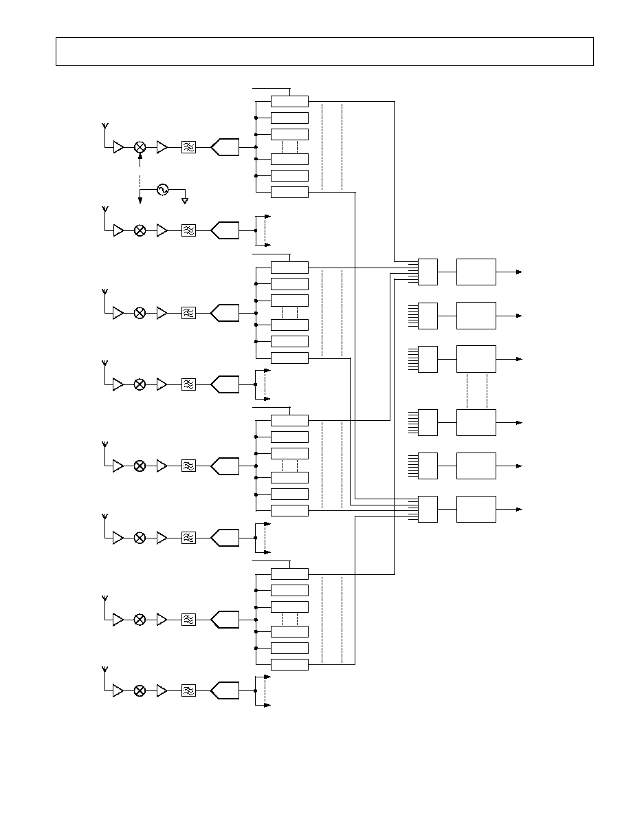
AD6640
REV. 0
23
Figure 52. Receive Chain for a Phased Array Cellular Base Station with Eight Antennas and 32 Channels
AD6640
COMMON LO
ANTENNA 1
EIGHT WIDEBAND FRONT ENDS
AD6620 (1)
SYNC 1
ANTENNA 2
AD6620s (32 CHANNELS)
AD6640
AD6640
ANTENNA 3
ANTENNA 4
AD6620s (32 CHANNELS)
AD6640
AD6640
ANTENNA 5
ANTENNA 6
AD6620s (32 CHANNELS)
AD6640
ANTENNA 8
AD6620s (32 CHANNELS)
AD6640
SUM
ADSP-21xx
(32)
SUM
ADSP-21xx
(31)
SUM
ADSP-21xx
(30)
SUM
ADSP-21xx
(3)
SUM
ADSP-21xx
(2)
SUM
ADSP-21xx
(1)
32 CHANNELS OUT
EACH CHANNEL IS SUMMATION
FROM EIGHT ANTENNA'S
COMBINE SIGNALS
FROM EIGHT ANTENNA'S
AD6620 (2)
AD6620 (3)
AD6620 (30)
AD6620 (31)
AD6620 (32)
AD6620 (1)
SYNC 1
AD6620 (2)
AD6620 (3)
AD6620 (30)
AD6620 (31)
AD6620 (32)
AD6620 (1)
SYNC 1
AD6620 (2)
AD6620 (3)
AD6620 (30)
AD6620 (31)
AD6620 (32)
AD6640
ANTENNA 7
AD6620 (1)
SYNC 1
AD6620 (2)
AD6620 (3)
AD6620 (30)
AD6620 (31)
AD6620 (32)
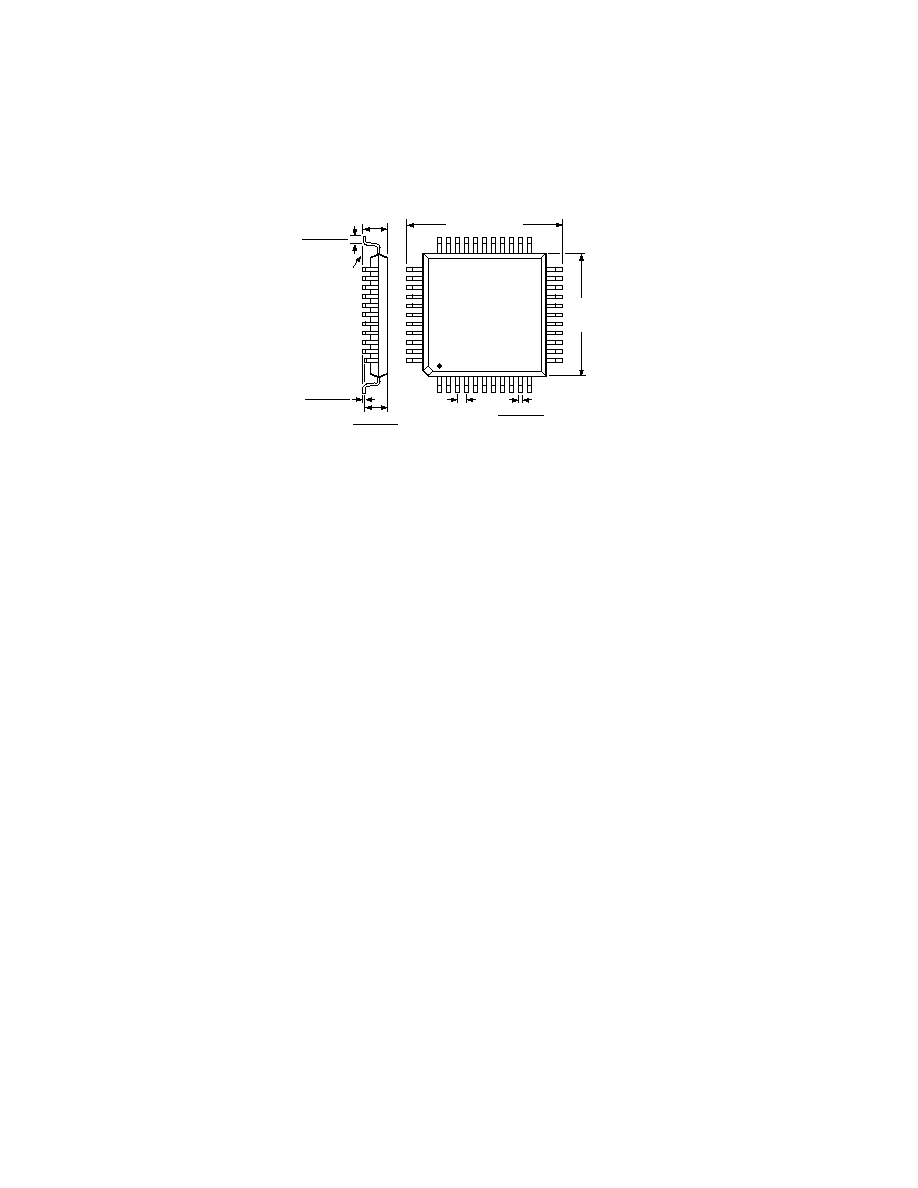
AD6640
24
REV. 0
C314181/98
PRINTED IN U.S.A.
AD6640AST OUTLINE DIMENSIONS
Dimensions shown in inches and (mm)
44-Terminal Plastic Thin Quad Flatpack
(ST-44)
TOP VIEW
(PINS DOWN)
1
33
34
44
11
12
23
22
0.018 (0.45)
0.012 (0.30)
0.031 (0.80)
BSC
0.394
(10.0)
SQ
0.472 (12.00) SQ
0.057 (1.45)
0.053 (1.35)
0.006 (0.15)
0.002 (0.05)
SEATING
PLANE
0.063 (1.60)
MAX
0.030 (0.75)
0.018 (0.45)