 | ÐлекÑÑоннÑй компоненÑ: AD7226 | СкаÑаÑÑ:  PDF PDF  ZIP ZIP |
Äîêóìåíòàöèÿ è îïèñàíèÿ www.docs.chipfind.ru
REV. A
Information furnished by Analog Devices is believed to be accurate and
reliable. However, no responsibility is assumed by Analog Devices for its
use, nor for any infringements of patents or other rights of third parties
which may result from its use. No license is granted by implication or
otherwise under any patent or patent rights of Analog Devices.
a
LC
2
MOS
Quad 8-Bit D/A Converter
AD7226
One Technology Way, P.O. Box 9106, Norwood, MA 02062-9106, U.S.A.
Tel: 617/329-4700
Fax: 617/326-8703
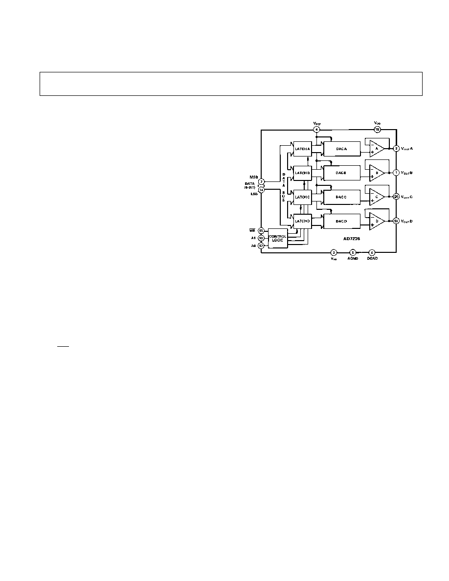
FUNCTIONAL BLOCK DIAGRAM
FEATURES
Four 8-Bit DACs with Output Amplifiers
Skinny 20-Pin DIP, SOIC and 20-Terminal
Surface Mount Packages
Microprocessor Compatible
TTL/CMOS Compatible
No User Trims
Extended Temperature Range Operation
Single Supply Operation Possible
APPLICATIONS
Process Control
Automatic Test Equipment
Automatic Calibration of Large System Parameters,
e.g., Gain/Offset
PRODUCT HIGHLIGHTS
1. DAC-to-DAC Matching
Since all four DACs are fabricated on the same chip at the
same time, precise matching and tracking between the DACs
is inherent.
2. Single Supply Operation
The voltage mode configuration of the DACs allows the
AD7226 to be operated from a single power supply rail.
3. Microprocessor Compatibility
The AD7226 has a common 8-bit data bus with individual
DAC latches, providing a versatile control architecture for
simple interface to microprocessors. All latch enable signals
are level triggered.
4. Small Size
Combining four DACs and four op amps plus interface logic
into a 20-pin DIP or SOIC or a 20-terminal surface mount
package allows a dramatic reduction in board space require-
ments and offers increased reliability in systems using mul-
tiple converters. Its pinout is aimed at optimizing board
layout with all the analog inputs and outputs at one end of the
package and all the digital inputs at the other.
GENERAL DESCRIPTION
The AD7226 contains four 8-bit voltage-output digital-to-
analog converters, with output buffer amplifiers and interface
logic on a single monolithic chip. No external trims are required
to achieve full specified performance for the part.
Separate on-chip latches are provided for each of the four D/A
converters. Data is transferred into one of these data latches
through a common 8-bit TTL/CMOS (5 V) compatible input
port. Control inputs A0 and A1 determine which DAC is loaded
when WR goes low. The control logic is speed-compatible with
most 8-bit microprocessors.
Each D/A converter includes an output buffer amplifier capable
of driving up to 5 mA of output current. The amplifiers' offsets
are laser-trimmed during manufacture, thereby eliminating any
requirement for offset nulling.
Specified performance is guaranteed for input reference voltages
from +2 V to +12.5 V with dual supplies. The part is also speci-
fied for single supply operation at a reference of +10 V.
The AD7226 is fabricated in an all ion-implanted high speed
Linear Compatible CMOS (LC
2
MOS) process which has been
specifically developed to allow high speed digital logic circuits
and precision analog circuits to be integrated on the same chip.

REV. A
2
AD7226SPECIFICATIONS
DUAL SUPPLY
Parameter
K, B, T Versions
2
Units
Conditions/Comments
STATIC PERFORMANCE
Resolution
8
Bits
Total Unadjusted Error
±
2
LSB max
V
DD
= +15 V
±
5%, V
REF
= +10 V
Relative Accuracy
±
1
LSB max
Differential Nonlinearity
±
1
LSB max
Guaranteed Monotonic
Full Scale Error
±
1 1/2
LSB max
Full Scale Temperature Coefficient
±
20
ppm/
°
C typ
V
DD
= 14 V to 16.5 V, V
REF
= +10 V
Zero Code Error
±
30
mV max
Zero Code Error Temperature Coefficient
±
50
µ
V/
°
C typ
REFERENCE INPUT
Voltage Range
2 to (V
DD
4)
V min to V max
Input Resistance
2
k
min
Input Capacitance
3
65
pF min
Occurs when each DAC is loaded with all 0s.
300
pF max
Occurs when each DAC is loaded with all 1s.
DIGITAL INPUTS
Input High Voltage, V
INH
2.4
V min
Input Low Voltage, V
INL
0.8
V max
Input Leakage Current
±
1
µ
A max
V
IN
= 0 V or V
DD
Input Capacitance
8
pF max
Input Coding
Binary
DYNAMIC PERFORMANCE
Voltage Output Slew Rate
4
2.5
V/
µ
s min
Voltage Output Settling Time
4
Positive Full Scale Change
5
µ
s max
V
REF
= +10 V; Settling Time to
±
1/2 LSB
Negative Full Scale Change
7
µ
s max
V
REF
= +10 V; Settling Time to
±
1/2 LSB
Digital Crosstalk
50
nV secs typ
Minimum Load Resistance
2
k
min
V
OUT
= +10 V
POWER SUPPLIES
V
DD
Range
11.4/16.5
V min/V max
For Specified Performance
I
DD
13
mA max
Outputs Unloaded; V
IN
= V
INL
or V
INH
I
SS
11
mA max
Outputs Unloaded; V
IN
= V
INL
or V
INH
SWITCHING CHARACTERISTICS
4, 5
Address to Write Setup Time, t
AS
@ 25
°
C
0
ns min
T
MIN
to T
MAX
0
ns min
Address to Write Hold Time, t
AH
@ 25
°
C
10
ns min
T
MIN
to T
MAX
10
ns min
Data Valid to Write Setup Time, t
DS
@ 25
°
C
90
ns min
T
MIN
to T
MAX
100
ns min
Data Valid to Write Hold Time, t
DH
@ 25
°
C
10
ns min
T
MIN
to T
MAX
10
ns min
Write Pulse Width, t
WR
@ 25
°
C
150
ns min
T
MIN
to T
MAX
200
ns min
NOTES
1
Maximum possible reference voltage.
2
Temperature ranges are as follows:
K Version: 40
°
C to +85
°
C
B Version: 40
°
C to +85
°
C
T Version: 55
°
C to +125
°
C
3
Guanteed by design. Not production tested.
4
Sample Tested at 25
°
C to ensure compliance.
5
Switching Characteristics apply for single and dual supply operation.
Specifications subject to change without notice.
(V
DD
= 11.4 V to 16.5 V, V
SS
= 5 V 10%; AGND = DGND = O V; V
REF
= +2 V to (V
DD
4 V)
1
unless otherwise noted.
All specifications T
MIN
to T
MAX
unless otherwise noted.)

AD7226
REV. A
3
ORDERING GUIDE
Total
Temperature
Unadjusted
Package
Model
1
Range
Error
Option
2
AD7226KN
40
°
C to +85
°
C
±
2 LSB
N-20
AD7226KP
40
°
C to +85
°
C
±
2 LSB
P-20A
AD7226KR
40
°
C to +85
°
C
±
2 LSB
R-20
AD7226BQ
40
°
C to +85
°
C
±
2 LSB
Q-20
AD7226TQ
55
°
C to +125
°
C
±
2 LSB
Q-20
AD7226TE
55
°
C to +125
°
C
±
2 LSB
E-20A
NOTES
1
To order MIL-STD-883, Class B processed parts, add /883B to part number.
Contact your local sales office for Military data sheet, for U.S. Standard Military
Drawing (SMD), see DESC drawing #596287802.
2
E = Leadless Ceramic Chip Carrier; N = Plastic DIP;
P = Plastic Leaded Chip Carrier; Q = Cerdip; R = SOIC.
SINGLE SUPPLY
Parameter
K, B, T Versions
2
Units
Conditions/Comments
STATIC PERFORMANCE
Resolution
8
Bits
Total Unadjusted Error
±
2
LSB max
Differential Nonlinearity
±
1
LSB max
Guaranteed Monotonic
REFERENCE INPUT
Input Resistance
2
k
min
Input Capacitance
3
65
pF min
Occurs when each DAC is loaded with all 0s.
300
pF max
Occurs when each DAC is loaded with all 1s.
DIGITAL INPUTS
Input High Voltage, V
INH
2.4
V min
Input Low Voltage, V
INL
0.8
V max
Input Leakage Current
±
1
µ
A max
V
IN
= 0 V or V
DD
Input Capacitance
8
pF max
Input Coding
Binary
DYNAMIC PERFORMANCE
Voltage Output Slew Rate
4
2
V/
µ
s min
Voltage Output Settling Time
4
Positive Full Scale Change
5
µ
s max
Settling Time to
±
1/2 LSB
Negative Full Scale Change
20
µ
s max
Settling Time to
±
1/2 LSB
Digital Crosstalk
50
nV secs typ
Minimum Load Resistance
2
k
min
V
OUT
= +10 V
POWER SUPPLIES
V
DD
Range
14.25/15.75
V min/V max
For Specified Performance
I
DD
13
mA max
Outputs Unloaded; V
IN
= V
INL
or V
INH
NOTES
1
Maximum possible reference voltage.
2
Temperature ranges are as follows:
K Version: 40
°
C to +85
°
C
B Version: 40
°
C to +85
°
C
T Version: 55
°
C to +125
°
C
3
Guanteed by design. Not production tested.
4
Sample Tested at 25
°
C to ensure compliance.
5
Switching Characteristics apply for single and dual supply operation.
Specifications subject to change without notice.
(V
DD
= +15 V 5%; V
SS
= AGND = DGND = O V; V
REF
= +10 V
1
unless otherwise noted.
All specifications T
MIN
to T
MAX
unless otherwise noted.)
AD7226
REV. A
4
ABSOLUTE MAXIMUM RATINGS*
V
DD
to AGND . . . . . . . . . . . . . . . . . . . . . . . . . . 0.3 V, +17 V
V
DD
to DGND . . . . . . . . . . . . . . . . . . . . . . . . . . 0.3 V, +17 V
V
SS
to AGND . . . . . . . . . . . . . . . . . . . . . . . . . . . . . 7 V, V
DD
V
SS
to DGND . . . . . . . . . . . . . . . . . . . . . . . . . . . . . 7 V, V
DD
V
DD
to V
SS
. . . . . . . . . . . . . . . . . . . . . . . . . . . . . 0.3 V, +24 V
AGND to DGND . . . . . . . . . . . . . . . . . . . . . . . . 0.3 V, V
DD
Digital Input Voltage to DGND . . . . . . . 0.3 V, V
DD
+ 0.3 V
V
REF
to AGND . . . . . . . . . . . . . . . . . . . . . . . . . . 0.3 V, V
DD
V
OUT
to AGND
1
. . . . . . . . . . . . . . . . . . . . . . . . . . . . V
SS
, V
DD
Power Dissipation (Any Package) to +75
°
C . . . . . . . . 500 mW
Derates above 75
°
C by . . . . . . . . . . . . . . . . . . . . . 2.0 mW/
°
C
Operating Temperature
Commercial (K Version) . . . . . . . . . . . . . . 40
°
C to +85
°
C
Industrial (B Version) . . . . . . . . . . . . . . . . 40
°
C to +85
°
C
Extended (T Version) . . . . . . . . . . . . . . . 55
°
C to +125
°
C
Storage Temperature . . . . . . . . . . . . . . . . . . 65
°
C to +150
°
C
Lead Temperature (Soldering, 10 secs) . . . . . . . . . . . +300
°
C
NOTES
*Stresses above those listed under "Absolute Maximum Ratings" may cause
permanent damage to the device. This is a stress rating only and functional
operation of the device at these or any other conditions above those indicated in
the operational sections of this specification is not implied. Exposure to absolute
maximum rating conditions for extended periods may affect device reliability.
1
Outputs may be shorted to AGND provided that the power dissipation of the
package is not exceeded. Typically short circuit current to AGND is 60 mA.
WARNING!
ESD SENSITIVE DEVICE
CAUTION
ESD (electrostatic discharge) sensitive device. Electrostatic charges as high as 4000 V readily
accumulate on the human body and test equipment and can discharge without detection.
Although the AD7226 features proprietary ESD protection circuitry, permanent damage may
occur on devices subjected to high energy electrostatic discharges. Therefore, proper ESD
precautions are recommended to avoid performance degradation or loss of functionality.
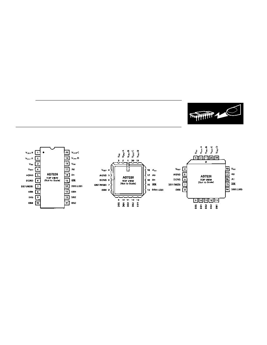
PIN CONFIGURATIONS
DIP and SOIC
LCCC
PLCC
TERMINOLOGY
TOTAL UNADJUSTED ERROR
This is a comprehensive specification which includes full-scale
error, relative accuracy and zero code error. Maximum output
voltage is V
REF
1 LSB (ideal), where 1 LSB (ideal) is V
REF
/
256. The LSB size will vary over the V
REF
range. Hence the zero
code error will, relative to the LSB size, increase as V
REF
de-
creases. Accordingly, the total unadjusted error, which includes
the zero code error, will also vary in terms of LSB's over the
V
REF
range. As a result, total unadjusted error is specified for a
fixed reference voltage of +10 V.
RELATIVE ACCURACY
Relative Accuracy or endpoint nonlinearity, is a measure of the
maximum deviation from a straight line passing through the
endpoints of the DAC transfer function. It is measured after al-
lowing for zero and full-scale error and is normally expressed in
LSB's or as a percentage of full-scale reading.
DIFFERENTIAL NONLINEARITY
Differential Nonlinearity is the difference between the measured
change and the ideal 1 LSB change between any two adjacent
codes. A specified differential nonlinearity of
±
1 LSB max over
the operating temperature range ensures monotonicity.
DIGITAL CROSSTALK
The glitch impulse transferred to the output of one converter
due to a change in the digital input code to another of the con-
verters. It is specified in nV secs and is measured at V
REF
= 0 V.
FULL SCALE ERROR
Full-Scale Error is defined as:
Measured Value Zero Code Error Ideal Value
AD7226
REV. A
5
CIRCUIT INFORMATION
D/A SECTION
The AD7226 contains four, identical, 8-bit, voltage mode
digital-to-analog converters. The output voltages from the con-
verters have the same polarity as the reference voltage allowing
single supply operation. A novel DAC switch pair arrangement
on the AD7226 allows a reference voltage range from +2 V to
+12.5 V.
Each DAC consists of a highly stable, thin-film, R-2R ladder
and eight high speed NMOS, single-pole, double-throw
switches. The simplified circuit diagram for one channel is
shown in Figure 1. Note that V
REF
(Pin 4) and AGND (Pin 5)
are common to all four DACs.
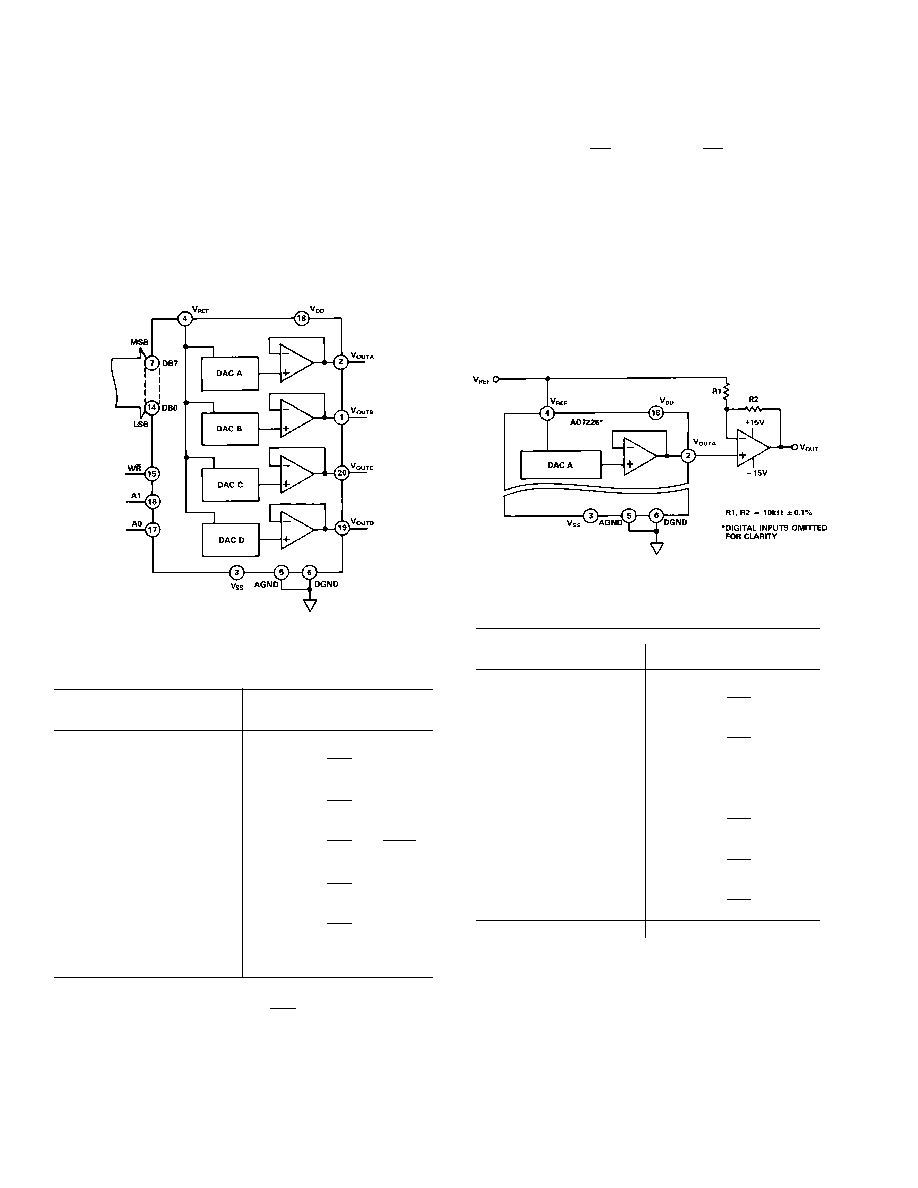
Figure 1. D/A Simplified Circuit Diagram
The input impedance at the V
REF
pin of the AD7226 is the par-
allel combination of the four individual DAC reference input
impedances. It is code dependent and can vary from 2 k
to in-
finity. The lowest input impedance (i.e., 2 k
) occurs when all
four DACs are loaded with the digital code 01010101. There-
fore, it is important that the reference presents a low output im-
pedance under changing load conditions. The nodal capacitance
at the reference terminals is also code dependent and typically
varies from 100 pF to 250 pF.
Each V
OUT
pin can be considered as a digitally programmable
voltage source with an output voltage of:
V
OUTX
= D
X
V
REF
where D
X
is fractional representation of the digital input code
and can vary from 0 to 255/256.
The source impedance is the output resistance of the buffer
amplifier.
OP AMP SECTION
Each voltage-mode D/A converter output is buffered by a unity
gain, noninverting CMOS amplifier. This buffer amplifier is
capable of developing +10 V across a 2 k
load and can drive
capacitive loads of 3300 pF. The output stage of this amplifier
consists of a bipolar transistor from the V
DD
line and a current
load to the V
SS
, the negative supply for the output amplifiers.
This output stage is shown in Figure 2.
The NPN transistor supplies the required output current drive
(up to 5 mA). The current load consists of NMOS transistors
which normally act as a constant current sink of 400
µ
A to V
SS
,
giving each output a current sink capability of approximately
400
µ
A if required.
The AD7226 can be operated single or dual supply resulting
in different performance in some parameters from the output
amplifiers.
In single supply operation (V
SS
= 0 V = AGND), with the out-
put approaching AGND (i.e., digital code approaching all 0s)
Figure 2. Amplifier Output Stage
the current load ceases to act as a current sink and begins to act
as a resistive load of approximately 2 k
to AGND. This occurs
as the NMOS transistors come out of saturation. This means
that, in single supply operation, the sink capability of the ampli-
fiers is reduced when the output voltage is at or near AGND. A
typical plot of the variation of current sink capability with out-
put voltage is shown in Figure 3.
Figure 3. Variation of I
SINK
with V
OUT
If the full sink capability is required with output voltages at or
near AGND (=0 V), then V
SS
can be brought below 0 V by 5 V
and thereby maintain the 400
µ
A current sink as indicated in
Figure 3. Biasing V
SS
below 0 V also gives additional headroom
in the output amplifier which allows for better zero code error
performance on each output. Also improved is the slew-rate
and negative-going settling-time of the amplifiers (discussed
later).
Each amplifier offset is laser trimmed during manufacture to
eliminate any requirement for offset nulling.
DIGITAL SECTION
The digital inputs of the AD7226 are both TTL and CMOS
(5 V) compatible from V
DD
= +11.4 V to +16.5 V. All logic in-
puts are static protected MOS gates with typical input currents
of less than 1 nA. Internal input protection is achieved by an
on-chip distributed diode from DGND to each MOS gate. To
minimize power supply currents, it is recommended that the
digital input voltages be driven as close to the supply rails (V
DD
and DGND) as practically possible.
AD7226
REV. A
6
INTERFACE LOGIC INFORMATION
Address lines A0 and A1 select which DAC will accept data
from the input port. Table I shows the selection table for the
four DACs with Figure 4 showing the input control logic. When
the WR signal is LOW, the input latches of the selected DAC
are transparent and its output responds to activity on the data
bus. The data is latched into the addressed DAC latch on the
rising edge of WR. While WR is high the analog outputs remain
at the value corresponding to the data held in their respective
latches.
Table I. AD7226 Truth Table
AD7226 Control Inputs
AD7226
WR
A1
A0
Operation
H
X
X
No Operation Device Not Selected
L
L
L
DAC A Transparent
g
L
L
DAC A Latched
L
L
H
DAC B Transparent
g
L
H
DAC B Latched
L
H
L
DAC C Transparent
g
H
L
DAC C Latched
L
H
H
DAC D Transparent
g
H
H
DAC D Latched
L = Low State, H = High State, X = Don't Care
Figure 4. Input Control Logic
Figure 5. Write Cycle Timing Diagram
Typical Performance Characteristics
(T
A
= 25 C, V
DD
= +15 V, V
SS
= 5 V)
Figure 6. Channel-to-Channel Matching
Figure 7. Relative Accuracy vs. V
REF
Figure 8. Differential Nonlinearity vs. V
REF
AD7226
REV. A
7
Figure 10. Dynamic Response (V
SS
= 5 V)
Figure 11a. Positive-Step Settling-Time (V
SS
= 5 V)
Figure 11b. Negative-Step Settling-Time (V
SS
= 5 V)
GROUND MANAGEMENT
AC or transient voltages between AGND and DGND can cause
noise at the analog output. This is especially true in micropro-
cessor systems where digital noise is prevalent. The simplest
method of ensuring that voltages at AGND and DGND are
equal is to tie AGND and DGND together at the AD7226. In
more complex systems where the AGND and DGND intertie is
on the backplane, it is recommended that two diodes be con-
nected in inverse parallel between the AD7226 AGND and
DGND pins (IN914 or equivalent).
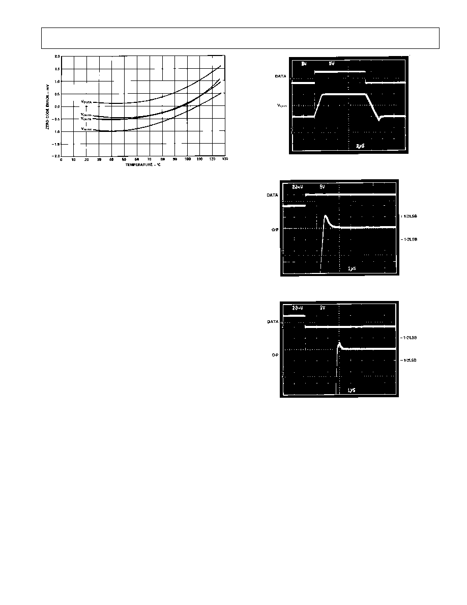
Figure 9. Zero Code Error vs. Temperature
SPECIFICATION RANGES
In order for the DACs to operate to their specifications, the ref-
erence voltage must be at least 4 V below the V
DD
power supply
voltage. This voltage differential is required for correct genera-
tion of bias voltages for the DAC switches.
The AD7226 is specified to operate over a V
DD
range from
+12 V
±
5% to +15 V
±
10% (i.e., from +11.4 V to +16.5 V)
with a V
SS
of 5 V
±
10%. Operation is also specified for a
single +15 V
±
5% V
DD
supply. Applying a V
SS
of 5 V results
in improved zero code error, improved output sink capability
with outputs near AGND and improved negative-going settling-
time.
Performance is specified over a wide range of reference voltages
from 2 V to (V
DD
4 V) with dual supplies. This allows a range
of standard reference generators to be used such as the AD580,
a +2.5 V bandgap reference and the AD584, a precision +10 V
reference. Note that in order to achieve an output voltage range
of 0 V to +10 V a nominal +15 V
±
5% power supply voltage is
required by the AD7226.
SETTLING TIME
The output stage of the buffer amplifiers consists of a bipolar
NPN transistor from the V
DD
line and a constant current load to
V
SS
. V
SS
is the negative power supply for the output buffer am-
plifiers. As mentioned in the op amp section, in single supply
operation the NMOS transistor will come out of saturation as
the output voltage approaches AGND and will act as a resistive
load of approximately 2 k
to AGND. As a result, the settling-
time for negative-going signals approaching AGND in single
supply operation will be longer than for dual supply operation
where the current load of 400
µ
A is maintained all the way down
to AGND. Positive-going settling-time is not affected by V
SS
.
The settling-time for the AD7226 is limited by the slew-rate of
the output buffer amplifiers. This can be seen from Figure 10
which shows the dynamic response for the AD7226 for a full
scale change. Figures 11a and 11b show expanded settling-time
photographs with the output waveforms derived from a differen-
tial input to an oscilloscope. Figure 11a shows the settling-time
for a positive-going step and Figure 11b shows the settling-time
for a negative-going output step.
AD7226
REV. A
8
Unipolar Output Operation
This is the basic mode of operation for each channel of the
AD7226, with the output voltage having the same positive
polarity as +V
REF
. The AD7226 can be operated single supply
(V
SS
= AGND) or with positive/negative supplies (see op-amp
section which outlines the advantages of having negative V
SS
).
The code table for unipolar output operation is shown in Table
II. Note that the voltage at V
REF
must never be negative with re-
spect to DGND in order to prevent parasitic transistor turn-on.
Connections for the unipolar output operation are shown in Fig-
ure 12.
Figure 12. AD7226 Unipolar Output Circuit
Table II. Unipolar Code Table
DAC Latch Contents
MSB
LSB
Analog Output
1 1 1 1
1 1 1 1
+
V
REF
255
256
1 0 0 0
0 0 0 1
+
V
REF
129
256
1 0 0 0
0 0 0 0
+
V
REF
128
256
= +
V
REF
2
0 1 1 1
1 1 1 1
+
V
REF
127
256
0 0 0 0
0 0 0 1
+
V
REF
1
256
0 0 0 0
0 0 0 0
0 V
Note: 1 LSB
=
V
REF
(
)
2
-
8
( )
=
V
REF
1
256
Bipolar Output Operation
Each of the DACs of the AD7226 can be individually config-
ured to provide bipolar output operation. This is possible using
one external amplifier and two resistors per channel. Figure 13
shows a circuit used to implement offset binary coding (bipolar
operation) with DAC A of the AD7226. In this case
V
OUT
=
1
+
R2
R1
D
A
V
REF
(
)
R2
R1
V
REF
(
)
With R1 = R2
V
OUT
= (2 D
A
1) · V
REF
where D
A
is a fractional representation of the digital word in
latch A.
Mismatch between R1 and R2 causes gain and offset errors and
therefore these resistors must match and track over temperature.
Once again the AD7226 can be operated in single supply or
from positive/negative supplies. Table III shows the digital code
versus output voltage relationship for the circuit of Figure 13
with R1 = R2.
Figure 13. AD7226 Bipolar Output Circuit
Table III. Bipolar (Offset Binary) Code Table
DAC Latch Contents
MSB
LSB
Analog Output
1 1 1 1
1 1 1 1
+
V
REF
127
128
1 0 0 0
0 0 0 1
+
V
REF
1
128
1 0 0 0
0 0 0 0
0 V
0 1 1 1
1 1 1 1
V
REF
1
128
0 0 0 0
0 0 0 1
V
REF
127
128
0 0 0 0
0 0 0 0
V
REF
128
128
=
V
REF
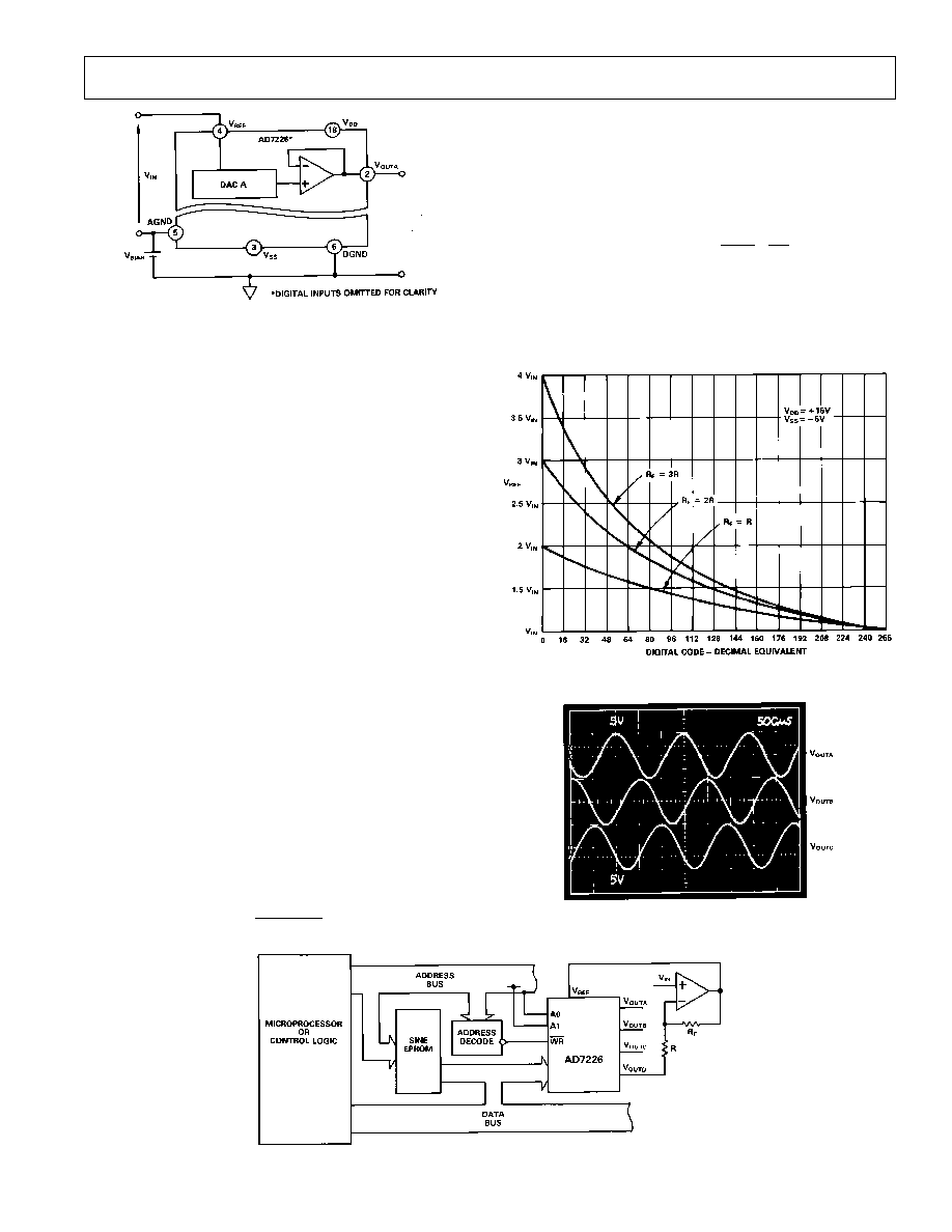
AGND BIAS
The AD7226 AGND pin can be biased above system GND
(AD7226 DGND) to provide an offset "zero" analog output
voltage level. Figure 14 shows a circuit configuration to achieve
this for channel A of the AD7226. The output voltage, V
OUTA
,
can be expressed as:
V
OUTA
= V
BIAS
+ D
A
(V
IN
)
where D
A
is a fractional representation of the digital input
word (0
D
255/256).
AD7226
REV. A
9
Figure 14. AGND Bias Circuit
For a given V
IN
, increasing AGND above system GND will re-
duce the effective V
DD
V
REF
which must be at least 4 V to en-
sure specified operation. Note that because the AGND pin is
common to all four DACs, this method biases up the output
voltages of all the DACs in the AD7226. Note that V
DD
and V
SS
of the AD7226 should be referenced to DGND.
3-PHASE SINE WAVE
The circuit of Figure 15 shows an application of the AD7226 in
the generation of 3-phase sine waves which can be used to con-
trol small 3-phase motors. The proper codes for synthesizing a
full sine wave are stored in EPROM, with the required phase-
shift of 120
°
between the three D/A converter outputs being
generated in software.
Data is loaded into the three D/A converters from the sine
EPROM via the microprocessor or control logic. Three loops
are generated in software with each D/A converter being loaded
from a separate loop. The loops run through the look-up table
producing successive triads of sinusoidal values with 120
°
sepa-
ration which are loaded to the D/A converters producing 3 sine
wave voltages 120
°
apart. A complete sine wave cycle is gener-
ated by stepping through the full look-up table. If a 256-element
sine wave table is used then the resolution of the circuit will be
1.4
°
(360
°
/256). Figure 17 shows typical resulting waveforms.
The sine waves can be smoothed by filtering the D/A converter
outputs.
The fourth D/A converter of the AD7226, DAC D, may be used
in a feedback configuration to provide a programmable refer-
ence voltage for itself and the other three converters. This con-
figuration is shown in Figure 15. The relationship of V
REF
to V
IN
is dependent upon digital code and upon the ratio of R
F
to R
and is given by the formula
V
REF
=
(1
+
G)
(1
+
G. D
D
)
V
IN
where G = R
F
/R
and D
D
is a fractional representation of the digital word
in latch D.
Alternatively, for a given V
IN
and resistance ratio, the required
value of D
D
for a given value of V
REF
can be determined from
the expression
D
D
=
(1
+
R / R
F
)
V
IN
V
REF
R
R
F
Figure 16 shows typical plots of V
REF
versus digital code for
three different values of R
F
. With V
IN
= +2.5 V and R
F
= 3 R
the peak-to-peak sine wave voltage from the converter outputs
will vary between +2.5 V and +10 V over the digital input code
range of 0 to 255.
Figure 16. Variation of V
REF
with Feedback Configuration
Figure 17. 3-Phase Sine Wave Output
Figure 15. 3-Phase Sine Wave Generation Circuit
AD7226
REV. A
10
STAIRCASE WINDOW COMPARATOR
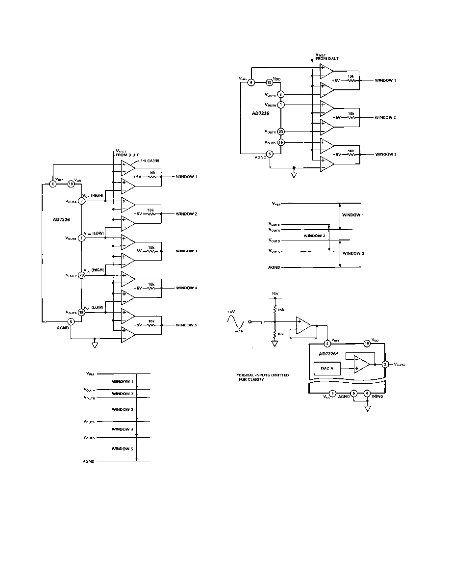
In many test systems, it is important to be able to determine
whether some parameter lies within defined limits. The staircase
window comparator of Figure 18a is a circuit which can be
used, for example, to measure the V
OH
and V
OL
thresholds of a
TTL device under test. Upper and lower limits on both V
OH
and V
OL
can be programmably set using the AD7226. Each ad-
jacent pair of comparators forms a window of programmable
size. If V
TEST
lies within a window then the output for that win-
dow will be high. With a reference of +2.56 V applied to the
V
REF
input, the minimum window size is 10 mV.
Figure 18a. Logic Level Measurement
Figure 18b. Window Structure
The circuit can easily be adapted to allow for overlapping of
windows as shown in Figure 19a. If the three outputs from this
circuit are decoded then five different nonoverlapping program-
mable windows can again be defined.
Figure 19a. Overlapping Windows
Figure 19b. Window Structure
Figure 20. Varying Reference Signal
VARYING REFERENCE SIGNAL
In some applications, it may be desirable to have a varying sig-
nal applied to the reference input of the AD7226. The AD7226
has multiplying capability within upper and lower limits of refer-
ence voltage when operated with dual supplies. The upper and
lower limits are those required by the AD7226 to achieve its lin-
earity specification. Figure 20 shows a sine wave signal applied
to the reference input of the AD7226. For input signal frequen-
cies up to 50 kHz the output distortion typically remains less
than 0.1%. Typical 3 dB bandwidth figure is 700 kHz.
AD7226
REV. A
11
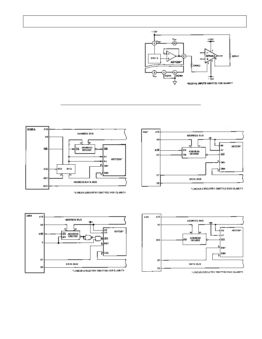
OFFSET ADJUST
Figure 21 shows how the AD7226 can be used to provide pro-
grammable input offset voltage adjustment for the AD544 op
amp. Each output of the AD7226 can be used to trim the input
offset voltage on one AD544. The 620 k
resistor tied to +10 V
provides a fixed bias current to one offset node. For symmetrical
adjustment, this bias current should equal the current in the
other offset node with the half-full scale code (i.e., 10000000)
on the DAC. Changing the code on the DAC varies the bias
current and hence provides offset adjust for the AD544. For ex-
ample, the input offset voltage on the AD544J, which has a
maximum of
±
2 mV, can be programmably trimmed to
±
10
µ
V.
Figure 21. Offset Adjust for AD544
Microprocessor Interface
Figure 22. AD7226 to 8085A Interface
Figure 23. AD7226 to 6809 Interface
Figure 24. AD7226 to 6502 Interface
Figure 25. AD7226 to Z-80 Interface
AD7226
REV. A
12
C812b85/87
PRINTED IN U.S.A.
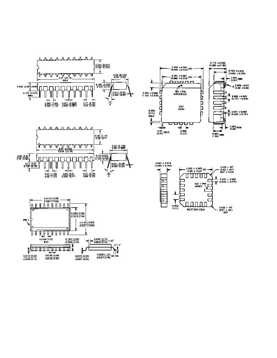
OUTLINE DIMENSIONS
Dimensions shown in inches and (mm).
20-Pin Plastic (N-20)
20-Pin Cerdip (Q-20)
20-Pin SOIC (R-20)
20-Terminal Plastic Leaded
Chip Carrier (P-20A)
20-Terminal Leadless
Ceramic Chip Carrier (E-20A)