 | ÐлекÑÑоннÑй компоненÑ: AD7233 | СкаÑаÑÑ:  PDF PDF  ZIP ZIP |
Äîêóìåíòàöèÿ è îïèñàíèÿ www.docs.chipfind.ru
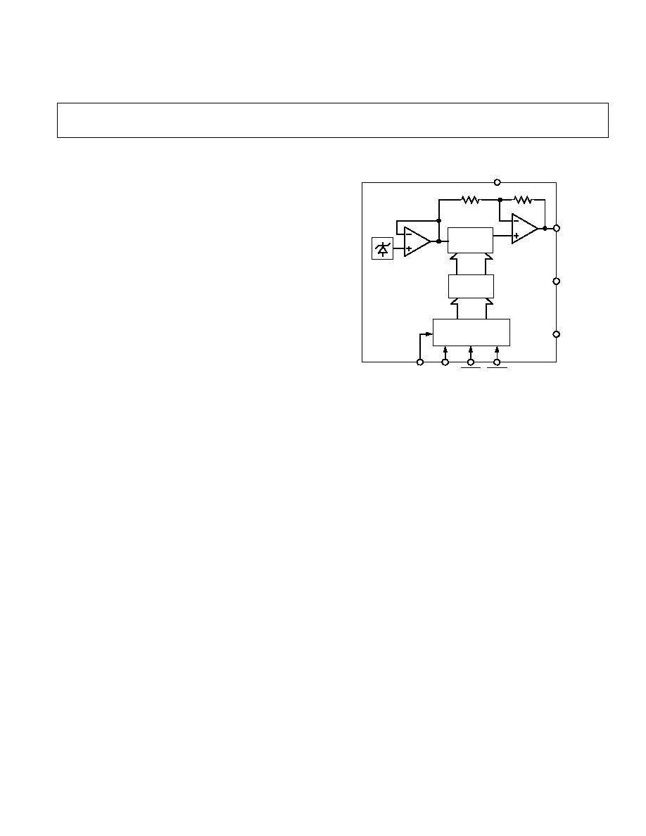
FUNCTIONAL BLOCK DIAGRAM
AD7233
DAC
LATCH
V
DD
V
SS
12
12
GND
LDAC
SDIN SCLK SYNC
12-BIT
DAC
2R
2R
V
OUT
INPUT SHIFT
REGISTER
REV. A
Information furnished by Analog Devices is believed to be accurate and
reliable. However, no responsibility is assumed by Analog Devices for its
use, nor for any infringements of patents or other rights of third parties
which may result from its use. No license is granted by implication or
otherwise under any patent or patent rights of Analog Devices.
a
LC
2
MOS
12-Bit Serial Mini-DIP DACPORT
AD7233
GENERAL DESCRIPTION
The AD7233 is a complete 12-bit, voltage-output, digital-to-
analog converter with output amplifier and Zener voltage refer-
ence all in an 8-lead package. No external trims are required to
achieve full specified performance. The data format is two's
complement, and the output range is 5 V to +5 V.
The AD7233 features a fast, versatile serial interface which al-
lows easy connection to both microcomputers and 16-bit digital
signal processors with serial ports. When the
SYNC input is
taken low, data on the SDIN pin is clocked into the input shift
register on each falling edge of SCLK. On completion of the
16-bit data transfer, bringing
LDAC low updates the DAC latch
with the lower 12 bits of data and updates the output. Alterna-
tively,
LDAC can be tied permanently low, and in this case the
DAC register is automatically updated with the contents of the
shift register when all sixteen data bits have been clocked in.
The serial data may be applied at rates up to 5 MHz allowing a
DAC update rate of 300 kHz.
For applications which require greater flexibility and unipolar
output ranges with single supply operation, please refer to the
AD7243 data sheet.
The AD7233 is fabricated on Linear Compatible CMOS
(LC
2
MOS), an advanced, mixed-technology process. It is pack-
aged in an 8-lead DIP package.
PRODUCT HIGHLIGHTS
1. Complete 12-Bit DACPORT
®
.
2. The AD7233 is a complete, voltage output, 12-bit DAC on a
single chip. This single-chip design is inherently more reli-
able than multichip designs.
3. Simple 3-wire interface to most microcontrollers and DSP
processors.
4. DAC Update Rate--300 kHz.
5. Space Saving 8-Lead Package.
FEATURES
12-Bit CMOS DAC with
On-Chip Voltage Reference
Output Amplifier
5 V to +5 V Output Range
Serial Interface
300 kHz DAC Update Rate
Small Size: 8-Pin Mini-DIP
Nonlinearity: 1/2 LSB T
MIN
to T
MAX
Low Power Dissipation: 100 mW typ
APPLICATIONS
Process Control
Industrial Automation
Digital Signal Processing Systems
Input/Output Ports
One Technology Way, P.O. Box 9106, Norwood, MA 02062-9106, U.S.A.
Tel: 781/329-4700
World Wide Web Site: http://www.analog.com
Fax: 781/326-8703
© Analog Devices, Inc., 2000
DACPORT is a registered trademark of Analog Devices, Inc.
REV. A
2
AD7233SPECIFICATIONS
1
(V
DD
= +12 V to +15 V,
2
V
SS
= 12 V to 15 V,
2
GND = 0 V, R
L
= 2 k
,
C
L
= 100 pF to GND. All specifications T
MIN
to T
MAX
unless otherwise noted.)
Parameter
A, B
Unit
Test Conditions/Comments
STATIC PERFORMANCE
Resolution
12
Bits
Relative Accuracy
3
±1
LSB max
Differential Nonlinearity
3
±0.9
LSB max
Guaranteed Monotonic
Bipolar Zero Error
3
±6
LSB max
DAC Latch Contents 0000 0000 0000
Full-Scale Error
3
±8
LSB max
Full-Scale Temperature Coefficient
4
±30
ppm of FSR/
°C typ
Guaranteed By Process
DIGITAL INPUTS
Input High Voltage, V
INH
2.4
V min
Input Low Voltage, V
INL
0.8
V max
Input Current
I
IN
±1
µA max
V
IN
= 0 V to V
DD
Input Capacitance
4
8
pF max
ANALOG OUTPUTS
Output Voltage Range
±5
V
DC Output Impedance
4
0.5
typ
AC CHARACTERISTICS
4
Voltage Output Settling Time
Settling Time to Within
±1/2 LSB of Final Value
Positive Full-Scale Change
10
µs max
Typically 4
µs; DAC Latch 100. . .000 to 011. . .111
Negative Full-Scale Change
10
µs max
Typically 5
µs; DAC Latch 011. . .111 to 100. . .000
Digital-to-Analog Glitch Impulse
3
30
nV secs typ
DAC Latch Contents Toggled Between All 0s and all 1s
Digital Feedthrough
3
10
nV secs typ
LDAC = High
POWER REQUIREMENTS
V
DD
Range
+10.8/+16.5
V min/V max
For Specified Performance Unless Otherwise Stated
V
SS
Range
10.8/16.5
V min/V max
For Specified Performance Unless Otherwise Stated
I
DD
10
mA max
Output Unloaded; Typically 7 mA at Thresholds
I
SS
2
mA max
Output Unloaded; Typically 1 mA at Thresholds
NOTES
1
Temperature Ranges are as follows: A, B Versions: 40
°C to +85°C.
2
Power Supply Tolerance: A, B Versions:
±10%.
3
See Terminology.
4
Guaranteed by design and characterization, not production tested.
Specifications subject to change without notice.
TIMING CHARACTERISTICS
1, 2
Limit at +25 C, T
MIN
, T
MAX
Parameter
(All Versions)
Unit
Conditions/Comments
t
1
3
200
ns min
SCLK Cycle Time
t
2
15
ns min
SYNC to SCLK Falling Edge Setup Time
t
3
70
ns min
SYNC to SCLK Hold Time
t
4
0
ns min
Data Setup Time
t
5
40
ns min
Data Hold Time
t
6
0
ns min
SYNC High to LDAC Low
t
7
20
ns min
LDAC Pulsewidth
t
8
0
ns min
LDAC High to SYNC Low
NOTES
1
Sample tested at +25
°C to ensure compliance. All input signals are specified with tr and tf = 5 ns (10% to 90% of 5 V) and timed from a voltage level of 1.6 V.
2
See Figure 3.
3
SCLK Mark/Space Ratio range is 40/60 to 60/40.
(V
DD
= +10.8 V to +16.5 V, V
SS
= 10.8 V to 16.5 V, GND = O V, R
L
= 2 k
,
C
L
= 100 pF. All Specifications T
MIN
to T
MAX
unless otherwise noted.)

AD7233
REV. A
3
ABSOLUTE MAXIMUM RATINGS
1
(T
A
= +25
°C unless otherwise noted)
V
DD
to GND . . . . . . . . . . . . . . . . . . . . . . . . . 0.3 V to +17 V
V
SS
to GND . . . . . . . . . . . . . . . . . . . . . . . . . . +0.3 V to 17 V
V
OUT
2
to GND . . . . . . . . . . . . . . . . . . . . 6 V to V
DD
+0.3 V
Digital Inputs to GND . . . . . . . . . . . . . 0.3 V to V
DD
+0.3 V
Operating Temperature Range
Industrial (A, B Versions) . . . . . . . . . . . . . 40
°C to +85°C
Storage Temperature Range . . . . . . . . . . . 65
°C to +150°C
Lead Temperature (Soldering, 10 secs) . . . . . . . . . . . . +300
°C
Power Dissipation to +75
°C . . . . . . . . . . . . . . . . . . . 450 mW
Derates above +75
°C by . . . . . . . . . . . . . . . . . . . . 10 mW/°C
ESD Rating . . . . . . . . . . . . . . . . . . . . . . . . . . . . . . . . >4000 V
NOTES
1
Stresses above those listed under Absolute Maximum Ratings may cause perma-
nent damage to the device. This is a stress rating only; functional operation of the
device at these or any other conditions above those listed in the operational sections
of this specification is not implied. Exposure to absolute maximum rating condi-
tions for extended periods may affect device reliability.
2
The output may be shorted to voltages in this range provided the power dissipation
of the package is not exceeded. Short circuit current is typically 80 mA.
ORDERING GUIDE
Temperature
Relative
Package
Model
Range
Accuracy
Option*
AD7233AN
40
°C to +85°C
±1 LSB
N-8
AD7233BN
40
°C to +85°C
±1/2 LSB
N-8
*N = Plastic DIP.
TERMINOLOGY
RELATIVE ACCURACY (LINEARITY)
Relative accuracy, or endpoint linearity, is a measure of the
maximum deviation of the DAC transfer function from a straight
line passing through the endpoints of the transfer function. It is
measured after allowing for zero and full-scale errors and is ex-
pressed in LSBs or as a percentage of full-scale reading.
DIFFERENTIAL NONLINEARITY
Differential nonlinearity is the difference between the measured
change and the ideal 1 LSB change between any two adjacent
codes. A specified differential nonlinearity of
±1 LSB or less
over the operating temperature range ensures monotonicity.
BIPOLAR ZERO ERROR
Bipolar zero error is the voltage measured at V
OUT
when the
DAC is loaded with all 0s. It is due to a combination of offset
errors in the DAC, amplifier and mismatch between the internal
gain resistors around the amplifier.
FULL-SCALE ERROR
Full-scale error is a measure of the output error when the am-
plifier output is at full scale (full scale is either positive or nega-
tive full scale).
DIGITAL-TO-ANALOG GLITCH IMPULSE
This is the voltage spike that appears at the output of the DAC
when the digital code in the DAC latch changes before the out-
put settles to its final value. The energy in the glitch is specified
in nV secs, and is measured for an all codes change (0000 0000
0000 to 1111 1111 1111).
DIGITAL FEEDTHROUGH
This is a measure of the voltage spike that appears on V
OUT
as a
result of feedthrough from the digital inputs on the AD7233. It
is measured with
LDAC held high.
AD7233
REV. A
4
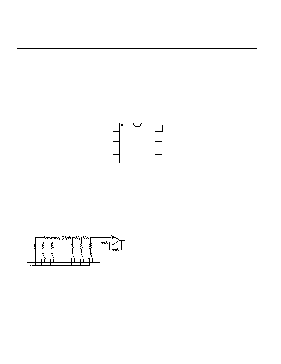
PIN FUNCTION DESCRIPTION
Pin
Mnemonic
Description
1
V
DD
Positive Supply (+12 V to +15 V).
2
SCLK
Serial Clock, Logic Input. Data is clocked into the input register on each falling SCLK edge.
3
SDIN
Serial Data In, Logic Input. The 16-bit serial data word is applied to this input.
4
SYNC
Data Synchronization Pulse, Logic Input. Taking this input low initializes the internal logic in
readiness for a new data word.
5
LDAC
Load DAC, Logic Input. Updates the DAC output. The DAC output is updated on the falling edge of
this signal, or alternatively if this line in permanently low, an automatic update mode is selected whereby
the DAC is updated on the 16th falling SCLK pulse.
6
GND
Ground Pin = 0 V.
7
V
OUT
Analog Output Voltage. This is the buffered DAC output voltage (5 V to +5 V).
8
V
SS
Negative Supply (12 V to 15 V).
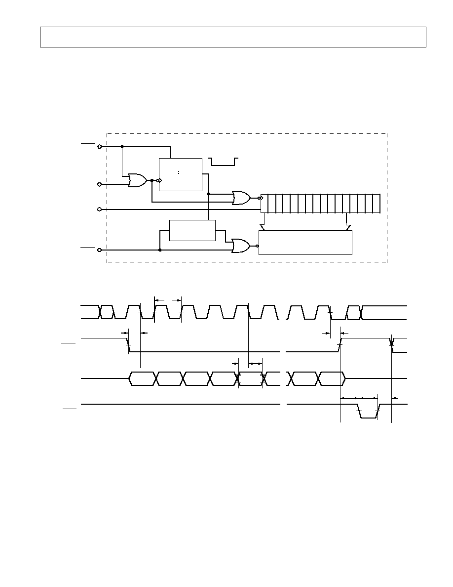
DIGITAL INTERFACE
The AD7233 contains an input serial to parallel shift register
and a DAC latch. A simplified diagram of the input loading cir-
cuitry is shown in Figure 2. Serial data on the SDIN input is
loaded to the input register under control of
SYNC and SCLK.
When a complete word is held in the shift register it may then be
loaded into the DAC latch under control of
LDAC. Only the
data in the DAC latch determines the analog output on the
AD7233.
A low
SYNC input provides the frame synchronization signal
which tells the AD7233 that valid serial data on the SDIN input
will be available for the next 16 falling edges of SCLK. An inter-
nal counter/decoder circuit provides a low gating signal so that
only 16 data bits are clocked into the input shift register. After
16 SCLK pulses the internal gating signal goes inactive (high)
thus locking out any further clock pulses. Therefore, either a
continuous clock or a burst clock source may be used to clock in
the data.
The
SYNC input should be taken high after the complete 16-bit
word is loaded in.
Although 16 bits of data are clocked into the input register, only
the latter 12 bits get transferred into the DAC latch. The first 4
bits in the 16-bit stream are don't cares since their value does
not affect the DAC latch data. Therefore the data format is 4
don't cares followed by the 12-bit data word with the LSB as the
last bit in the serial stream.
CIRCUIT INFORMATION
D/A Section
The AD7233 contains a 12-bit voltage-mode D/A converter
consisting of highly stable thin-film resistors and high speed
NMOS single-pole, double-throw switches.
Op Amp Section
The output of the voltage-mode D/A converter is buffered by a
noninverting CMOS amplifier. The buffer amplifier is capable
of developing
±5 V across a 2 k load to GND.
2R
R
2R
R
R
2R
2R
V
OUT
GND
2R
2R
2R
DB0
DB1
DB9
DB10 DB11
2R
R
R
INTERNAL
REFERENCE
5V
Figure 1. Simplified D/A Converter
V
OUT
LDAC
2
3
4
5
6
7
8
AD7233
TOP VIEW
(Not to Scale)
GND
SDIN
SCLK
V
SS
V
DD
SYNC
1
AD7233
REV. A
5
There are two ways in which the DAC latch and hence the ana-
log output may be updated. The status of the
LDAC input is
examined after
SYNC is taken low. Depending on its status, one
of two update modes is selected.
If
LDAC = 0 then the automatic update mode is selected. In
this mode the DAC latch and analog output are updated auto-
matically when the last bit in the serial data stream is clocked in.
The update thus takes place on the sixteenth falling SCLK edge.
If
LDAC = 1 then the automatic update is disabled and the
DAC latch is updated by taking
LDAC low any time after the
16-bit data transfer is complete. The update now occurs on the
falling edge of
LDAC. This facility is useful for simultaneous
update in multi-DAC systems. Note that the
LDAC input must
be taken back high again before the next data transfer is initiated.
RESET
SCLK
16
COUNTER/
DECODER
GATING
SIGNAL
GATED
SCLK
SDIN
INPUT SHIFT REGISTER (16 BITS)
DAC LATCH (12 BITS)
SYNC
LDAC
AUTO-UPDATE
CIRCUITRY
Figure 2. Simplified Loading Structure
SCLK
SDIN
t
4
t
1
t
3
t
2
t
5
DB15
DON'T CARE
DB0
LSB
SYNC
LDAC
DB11
MSB
DB14
DON'T CARE
DB13
DON'T CARE
DB12
DON'T CARE
t
6
t
7
t
8
DB1
Figure 3. Timing Diagram