 | –≠–ª–µ–∫—Ç—Ä–æ–Ω–Ω—ã–π –∫–æ–º–ø–æ–Ω–µ–Ω—Ç: AD7376 | –°–∫–∞—á–∞—Ç—å:  PDF PDF  ZIP ZIP |
Document Outline
- Specifications
- Pinout
- Package Drawings
- Ordering Guide
- Features
- Applications
- Product Description
- Timing characteristics
- Absolute Maximum Ratings
- Functional Block Diagram
- Pin Function Description
- Typical Characteristics
- CAUTION
- OPERATION
- DIGITAL INTERFACING
- PROGRAMMING THE VARIABLE RESISTOR
- RDAC CIRCUIT SIMULATION MODEL
- PROGRAMMING THE POTENTIOMETER DIVIDER
- TEST CIRCUITS
- DIGITAL POTENTIOMETER FAMILY SELECTION GUIDE
- DIAGRAMS
- Timing Diagram
- Detail Timing Diagram
- Daisy-Chain Configuration Using SDO
- Block Diagram
- Detail SDO Output Schematic of the AD5207
- Equivalent RDAC Circuit
- Equivalent Input Control Logic
- ESD Protection of Digital Pins
- ESD Protection of Resistor Terminals
- RDAC Circuit Simulation Model for RDAC = 10 k.
- Potentiometer Divider Nonlinearity Error Test Circuit (INL, DNL)
- Noninverting Gain Test Circuit
- Resistor Position Nonlinearity Error (Rheostat Operation; R-INL, R-DNL)
- Gain vs. Frequency Test Circuit
- Wiper Resistance Test Circuit
- Incremental ON Resistance Test Circuit
- Power Supply Sensitivity Test Circuit (PSS, PSSR)
- Common-Mode Leakage Current Test Circuit
- Inverting Gain Test Circuit

REV. 0
Information furnished by Analog Devices is believed to be accurate and
reliable. However, no responsibility is assumed by Analog Devices for its
use, nor for any infringements of patents or other rights of third parties that
may result from its use. No license is granted by implication or otherwise
under any patent or patent rights of Analog Devices.
a
AD5207
One Technology Way, P.O. Box 9106, Norwood, MA 02062-9106, U.S.A.
Tel: 781/329-4700
www.analog.com
Fax: 781/326-8703
© Analog Devices, Inc., 2001
2-Channel, 256-Position
Digital Potentiometer
FUNCTIONAL BLOCK DIAGRAM
RDAC1 REGISTER
R
RDAC2 REGISTER
R
POWER-
ON
RESET
LOGIC
SERIAL INPUT REGISTER
AD5207
8
SDO
DGND
SDI
CS
V
SS
SHDN
V
DD
A1
W1
B1
A2
W2
B2
CLK
FEATURES
256-Position, 2-Channel
Potentiometer Replacement
10 k , 50 k , 100 k
Power Shut-Down, Less than 5 A
2.7 V to 5.5 V Single Supply
2.7 V Dual Supply
3-Wire SPI-Compatible Serial Data Input
Midscale Preset During Power-On
APPLICATIONS
Mechanical Potentiometer Replacement
Stereo Channel Audio Level Control
Instrumentation: Gain, Offset Adjustment
Programmable Voltage-to-Current Conversion
Programmable Filters, Delays, Time Constants
Line Impedance Matching
Automotive Electronics Adjustment
GENERAL DESCRIPTION
The AD5207 provides dual channel, 256-position, digitally
controlled variable resistor (VR) devices that perform the same
electronic adjustment function as a potentiometer or variable
resistor. Each channel of the AD5207 contains a fixed resistor with
a wiper contact that taps the fixed resistor value at a point
determined by a digital code loaded into the SPI-compatible
serial-input register. The resistance between the wiper and either
end point of the fixed resistor varies linearly with respect to the
digital code transferred into the VR latch. The variable resistor
offers a completely programmable value of resistance, between
the A Terminal and the wiper or the B Terminal and the wiper.
The fixed A-to-B terminal resistance of 10 k
, 50 k or 100 k
has a
±1% channel-to-channel matching tolerance with a nomi-
nal temperature coefficient of 500 ppm/
∞C. A unique switching
circuit minimizes the high glitch inherent in traditional switched
resistor designs and avoids any make-before-break or break-
before-make operation.
Each VR has its own VR latch, which holds its programmed
resistance value. These VR latches are updated from an internal
serial-to-parallel shift register, which is loaded from a standard
3-wire serial-input digital interface. Ten bits, to make up the
data word, are required and clocked into the serial input register.
The first two bits are address bits. The following eight bits are
the data bits that represent the 256 steps of the resistance value.
The reason for two address bits instead of one is to be compatible
with similar products such as AD8402 so that drop-in replacement
is possible. The address bit determines the corresponding VR
latch to be loaded with the data bits during the returned positive
edge of
CS strobe. A serial data output pin at the opposite end
of the serial register allows simple daisy chaining in multiple
VR applications without additional external decoding logic.
An internal reset block will force the wiper to the midscale posi-
tion during every power-up condition. The
SHDN pin forces an
open circuit on the A Terminal and at the same time shorts the
wiper to the B Terminal, achieving a microwatt power shutdown
state. When
SHDN is returned to logic high, the previous latch
settings put the wiper in the same resistance setting prior to
shutdown. The digital interface remains active during shutdown;
code changes can be made to produce new wiper positions when
the device is resumed from shutdown.
The AD5207 is available in 1.1 mm thin TSSOP-14 package,
which is suitable for PCMCIA applications. All parts are guaran-
teed to operate over the extended industrial temperature range
of ≠40
∞C to +125∞C.

REV. 0
≠2≠
AD5207≠SPECIFICATIONS
ELECTRICAL CHARACTERISTICS 10 k , 50 k , 100 k VERSION
(V
DD
= 5 V, V
SS
= 0, V
A
= 5 V,
V
B
= 0, ≠40 C < T
A
< +125 C unless otherwise noted.)
Parameter
Symbol
Conditions
Min
Typ
1
Max
Unit
DC CHARACTERISTICS
RHEOSTAT MODE
Specifications Apply to All VRs
Resistor Differential Nonlinearity
2
R-DNL
R
WB
, V
A
= NC
≠1
+1
LSB
Resistor Nonlinearity
2
R-INL
R
WB
, V
A
= NC
≠1.5
+1.5
LSB
Nominal Resistor Tolerance
3
R
≠30
+30
%
Resistance Temperature Coefficient
R
AB
/
T
V
AB
= V
DD
, Wiper = No Connect
500
ppm/
∞C
Wiper Resistance
R
W
I
W
= 1 V/R, V
DD
= 5 V
50
100
Nominal Resistance Match
R/R
O
Ch 1 to 2, V
AB
= V
DD
, T
A
= 25
∞C
0.2
1
%
DC CHARACTERISTICS
POTENTIOMETER DIVIDER MODE
Specifications Apply to All VRs
Resolution
N
8
Bits
Integral Nonlinearity
4
INL
≠1.5
+1.5
LSB
Differential Nonlinearity
4
DNL
V
DD
= 5 V, V
SS
= 0 V
≠1
+1
LSB
Voltage Divider Temperature
V
W
/
T
Code = 80
H
15
ppm/
∞C
Coefficient
Full-Scale Error
V
WFSE
Code = FF
H
≠1.5
LSB
Zero-Scale Error
V
WZSE
Code = 00
H
+1.5
LSB
RESISTOR TERMINALS
Voltage Range
5
V
A,
B, W
|V
DD
| + |V
SS
|
5.5 V
V
SS
V
DD
V
Capacitance
6
A
X
, B
X
C
A,B
f = 1 MHz, Measured to GND, Code = 80
H
45
pF
Capacitance
6
W
X
C
W
f = 1 MHz, Measured to GND, Code = 80
H
70
pF
Shutdown Current
7
I
A_SD
V
A
= V
DD
, V
B
= 0 V,
SHDN = 0
5
µA
Shutdown Wiper Resistance
R
W_SD
V
A
= V
DD
, V
B
= 0 V,
SHDN = 0, V
DD
= 5 V
200
Common-Mode Leakage
I
CM
V
A
= V
B
= V
DD
/2
1
nA
DIGITAL INPUTS AND OUTPUTS
Input Logic High
V
IH
V
DD
= 5 V, V
SS
= 0 V
2.4
V
Input Logic Low
V
IL
V
DD
= 5 V, V
SS
= 0 V
0.8
V
Input Logic High
V
IH
V
DD
= 3 V, V
SS
= 0 V
2.1
V
Input Logic Low
V
IL
V
DD
= 3 V, V
SS
= 0 V
0.6
V
Output Logic High
V
OH
R
L
= 1 k
to V
DD
V
DD
≠ 0.1
V
Output Logic Low
V
OL
I
OL
= 1.6 mA, V
DD
= 5 V
0.4
V
Input Current
I
IL
V
IN
= 0 V or 5 V
±10
µA
Input Capacitance
6
C
IL
10
pF
POWER SUPPLIES
Power Single-Supply Range
V
DD RANGE
V
SS
= 0 V
2.7
5.5
V
Power Dual-Supply Range
V
DD/SS RANGE
±2.2
±2.7
V
Positive Supply Current
I
DD
V
IH
= V
DD
or V
IL
= GND, V
SS
= 0 V
40
µA
Negative Supply Current
I
SS
V
IH
= V
DD
or V
IL
= GND V
SS
= ≠2.5 V
40
µA
Power Dissipation
8
P
DISS
V
IH
= 5 V or V
IL
= 0 V, V
DD
= 5 V
0.2
mW
Power Supply Sensitivity, V
DD
PSS
V
DD
= 5 V
± 10%, V
SS
= 0 V, Code = 80
H
0.01
%/%
Power Supply Sensitivity, V
SS
PSS
V
SS
= ≠2.5 V
± 10%, V
DD
= 2.5 V, Code = 80
H
0.03
%/%
DYNAMIC CHARACTERISTICS
6, 9
Bandwidth ≠3 dB
BW_10 k
R
AB
= 10 k
600
kHz
Bandwidth ≠3 dB
BW_50 k
R
AB
= 50 k
125
kHz
Bandwidth ≠3 dB
BW_100 k
R
AB
= 100 k
71
kHz
Total Harmonic Distortion
THD
W
V
A
= 1 V rms, V
B
= 0 V, f = 1 kHz, R
AB
= 10 k
0.003
%
V
W
Settling Time
t
S
R
AB
= 10 k
/50 k/100 k, ±1 LSB Error Band
2/9/18
µs
Resistor Noise Voltage
e
N_WB
R
WB
= 5 k
, f = 1 kHz, RS = 0
9
nV
Hz
Crosstalk
10
C
T
V
A
= 5 V, V
B
= 0 V
≠65
dB
REV. 0
≠3≠
AD5207
Parameter
Symbol
Conditions
Min
Typ
1
Max
Unit
INTERFACE TIMING
CHARACTERISTICS
Applies to All Parts
6, 11
Input Clock Pulsewidth
t
CH
, t
CL
Clock Level High or Low
10
ns
Data Setup Time
t
DS
5
ns
Data Hold Time
t
DH
5
ns
CLK to SDO Propagation Delay
12
t
PD
R
L
= 1 k
to 5 V, C
L
< 20 pF
1
25
ns
CS Setup Time
t
CSS
10
ns
CS High Pulsewidth
t
CSW
10
ns
CLK Fall to
CS Fall Hold Time
t
CSH0
0
ns
CLK Fall to
CS Rise Hold Time
t
CSH1
0
ns
CS Rise to Clock Rise Setup
t
CS1
10
ns
NOTES
1
Typicals represent average readings at 25
∞C and V
DD
= 5 V, V
SS
= 0 V.
2
Resistor position nonlinearity error R-INL is the deviation from an ideal value measured between the maximum resistance and the minimum resistance wiper
positions. R-DNL measures the relative step change from ideal between successive tap positions. Parts are guaranteed monotonic. I
W
= V
DD
/R for both V
DD
= 5 V,
V
SS
= 0 V.
3
V
AB
= V
DD
, Wiper (V
W
) = No connect.
4
INL and DNL are measured at V
W
with the RDAC configured as a potentiometer divider similar to a voltage output D/A converter. V
A
= V
DD
and V
B
= 0 V. DNL
specification limits of
±1 LSB maximum are Guaranteed Monotonic operating conditions.
5
Resistor Terminals A, B, W have no limitations on polarity with respect to each other.
6
Guaranteed by design and not subject to production test.
7
Measured at the A
X
terminals. All A
X
terminals are open-circuited in shut-down mode.
8
P
DISS
is calculated from (I
DD
◊ V
DD
). CMOS logic level inputs result in minimum power dissipation.
9
All dynamic characteristics use V
DD
= 5 V, V
SS
= 0 V.
10
Measured at a V
W
pin where an adjacent V
W
pin is making a full-scale voltage change.
11
See timing diagram for location of measured values. All input control voltages are specified with t
R
= t
F
= 2 ns (10% to 90% of 3 V) and timed from a voltage level of
1.5 V. Switching characteristics are measured using V
DD
= 5 V.
12
Propagation delay depends on value of V
DD
, R
L
, and C
L
; see applications text.
The AD5207 contains 474 transistors. Die Size: 67 mil
◊ 69 mil, 4623 sq. mil.
Specifications subject to change without notice.
1
0
1
0
1
0
SDI
CLK
CS
V
OUT
RDAC REGISTER LOAD
A1
A0
D7
D6
D5
D4
D3
D2
D1
D0
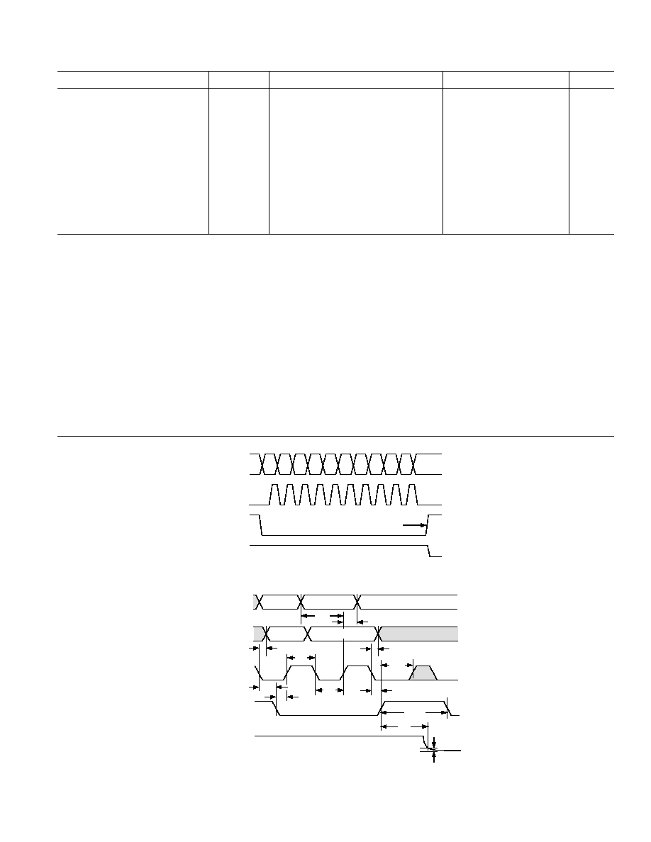
Figure 1a. Timing Diagram
1
0
1
0
1
0
1
0
V
DD
0V
SDI
(DATA IN)
SDO
(DATA OUT)
CLK
CS
V
OUT
Ax OR Dx
Ax OR Dx
A'x OR D'x
A
'
x OR D
'
x
1LSB ERROR BAND
1LSB
t
DS
t
DH
t
PD_MAX
t
CS1
t
CSH1
t
CSW
t
S
t
CL
t
CH
t
CSH0
t
CSS
Figure 1b. Detail Timing Diagram

REV. 0
AD5207
≠4≠
CAUTION
ESD (electrostatic discharge) sensitive device. Electrostatic charges as high as 4000 V readily
accumulate on the human body and test equipment and can discharge without detection. Although
the AD5207 features proprietary ESD protection circuitry, permanent damage may occur on
devices subjected to high-energy electrostatic discharges. Therefore, proper ESD precautions are
recommended to avoid performance degradation or loss of functionality.
WARNING!
ESD SENSITIVE DEVICE
ABSOLUTE MAXIMUM RATINGS
1
(T
A
= 25
∞C, unless otherwise noted)
V
DD
to GND . . . . . . . . . . . . . . . . . . . . . . . . . . . . . . ≠0.3, +7 V
V
SS
to GND . . . . . . . . . . . . . . . . . . . . . . . . . . . . . . . . . 0, ≠3 V
V
DD
to V
SS
. . . . . . . . . . . . . . . . . . . . . . . . . . . . . . . . . . . . . 7 V
V
A
, V
B
, V
W
to GND . . . . . . . . . . . . . . . . . . . . . . . . . . V
SS
, V
DD
I
MAX
2
(A, B, W) . . . . . . . . . . . . . . . . . . . . . . . . . . . . .
±20 mA
Digital Inputs and Output Voltage to GND . . 0 V, V
DD
+ 0.3 V
Operating Temperature Range . . . . . . . . . . ≠40
∞C to +125∞C
Maximum Junction Temperature (T
J
Max) . . . . . . . . . . 150
∞C
Storage Temperature . . . . . . . . . . . . . . . . . . ≠65
∞C to +150∞C
Lead Temperature (Soldering, 10 sec) . . . . . . . . . . . . . 300
∞C
Thermal Resistance
3
JA,
TSSOP-14 . . . . . . . . . . . . . 206
∞C/W
NOTES
1
Stresses above those listed under Absolute Maximum Ratings may cause perma-
nent damage to the device. This is a stress rating only; functional operation of the
device at these or any other conditions above those indicated in the operational
section of this specification is not implied. Exposure to absolute maximum rating
conditions for extended periods may affect device reliability.
2
Max current is bounded by the maximum current handling of the switches,
maximum power dissipation of the package, and maximum applied voltage
across any two of the A, B, and W Terminals at a given resistance. Please refer to
TPC 22 for detail.
3
Package Power Dissipation = (T
J
Max≠T
A
)/
JA
.
PIN FUNCTION DESCRIPTIONS
Pin
Mnemonic Description
1
V
SS
Negative Power Supply, specified for opera-
tion from 0 V to ≠2.7 V.
2
B2
Terminal B of RDAC#2.
3
A2
Terminal A of RDAC#2.
4
W2
Wiper, RDAC#2, addr = 1
2
5
DGND
Digital Ground.
6
SHDN
Active Low Input. Terminal A open-circuit
and Terminal B shorted to Wiper. Shut-
down controls both RDACs #1 and #2.
7
CS
Chip Select Input, Active Low. When
CS
returns high, data in the serial input register
is decoded, based on the address bit, and
loaded into the corresponding RDAC register.
8
SDI
Serial Data Input. MSB is loaded first.
9
SDO
Serial Data Output. Open Drain transistor
requires pull-up resistor.
10
CLK
Serial Clock Input. Positive Edge Triggered.
11
V
DD
Positive Power Supply. Specified for opera-
tion at 2.7 V to 5.5 V.
12
W1
Wiper, RDAC #1, addr = 0
2
.
13
A1
Terminal A of RDAC #1.
14
B1
Terminal B of RDAC #1.
Table I. Serial-Data Word Format
ADDR
DATA
B9
B8
B7
B6
B5
B4
B3
B2
B1
B0
A1
A0
D7
D6
D5
D4
D3
D2
D1
D0
MSB
LSB
2
9
2
8
2
7
2
0
NOTES
ADDR(RDAC1) = 00; ADDR(RDAC2 = 01).
Data loads B9 first into SDI pin.
PIN CONFIGURATION
TOP VIEW
(Not to Scale)
14
13
12
11
10
9
8
1
2
3
4
5
6
7
B1
V
SS
AD5207
A1
B2
W1
A2
V
DD
W2
CLK
DGND
SDO
SHDN
SDI
CS
ORDERING GUIDE
Temperature
Package
Package
Qty Per
Branding
Model
k
Range
Description
Option
Container
Information
*
AD5207BRU10-REEL7
10
≠40
∞C to +125∞C
TSSOP-14
RU-14
1,000
B10
AD5207BRU50-REEL7
50
≠40
∞C to +125∞C
TSSOP-14
RU-14
1,000
B50
AD5207BRU100-REEL7
100
≠40
∞C to +125∞C
TSSOP-14
RU-14
1,000
B100
*Three lines of information appear on the device. Line 1 lists the part number; Line 2 includes branding information and the ADI logo, and Line 3 contains the
date code YYWW.

REV. 0
≠5≠
Typical Performance Characteristics≠AD5207
CODE ≠ Decimal
0.20
RDNL ≠ LSB
224
0.15
0.10
0.05
0.00
0.05
0.10
0.15
0.20
192
160
128
96
64
32
0
256
V
DD
= 5.5V, V
SS
= 0V
TPC 1. 10 k
RDNL vs. Code
CODE ≠ Decimal
RINL
≠
LSB
224
≠0.15
≠0.10
≠0.05
0.00
0.10
0.20
192
160
128
96
64
32
0
256
≠0.20
0.15
0.05
V
DD
= 5.5V, V
SS
= 0V
TPC 2. 10 k
RINL vs. Code
CODE ≠ Decimal
DNL
≠
LSB
224
≠0.2
≠0.1
0.0
0.3
192
160
128
96
64
32
0
256
≠0.3
0.1
0.2
V
DD
= 5.5V, V
SS
= 0V
TPC 3. 10 k
DNL vs. Code
CODE ≠ Decimal
INL
≠
LSB
224
≠0.2
≠0.1
0.0
0.1
0.3
192
160
128
96
64
32
0
256
≠0.3
0.2
≠0.4
0.4
V
DD
= 5.5V, V
SS
= 0V
TPC 4. 10 k
INL vs. Code
V
IH
≠ V
I
DD
/I
SS
≠
mA
0.01
1.0
5.0
4.0
3.0
2.0
1.0
0.0
0.001
0.1
I
DD
@ V
DD
/V
SS
= 5V/0V
I
DD
@ V
DD
/V
SS
= 3V/0V
I
DD
@ V
DD
/V
SS
= 2.5V
I
SS
@ V
DD
/V
SS
= 2.5V
TPC 5. Supply Current vs. Logic Input Voltage
TEMPERATURE ≠ C
I
DD
SUPPL
Y CURRENT
≠
A
20
≠40
V
IL
= V
SS
V
IH
= V
DD
18
16
14
12
10
8
6
4
2
0
≠20
0
20
40
60
80
100
V
DD
= 5.5V
V
DD
= 2.7V
TPC 6. Supply Current vs. Temperature
REV. 0
AD5207
≠6≠
TEMPERATURE ≠ C
I
A_SD
SHUTDO
WN CURRENT
≠
nA
45
≠40
20
15
10
5
0
≠20
0
20
40
60
80
100
25
120
30
35
40
V
DD
= 5.5V
TPC 7. Shutdown Current vs. Temperature
V
SUPPLY
≠ V
R
ON
≠
160
0
6
140
120
100
80
60
40
20
0
5
4
3
2
1
V
DD
= 3V
V
DD
= 5V
TPC 8. Wiper ON Resistance vs. V
SUPPLY
FREQUENCY ≠ Hz
I
DD
/I
SS
≠
A
1000
10k
900
800
700
600
500
400
300
200
100
0
100k
1M
10M
CODE FF
H
I
SS
@ V
DD
/V
SS
= 2.5V
I
DD
@ V
DD
/V
SS
= 2.5V
I
DD
@ V
DD
/V
SS
= 5V/0V
I
DD
@ V
DD
/V
SS
= 3V/0V
TPC 9. 10 k
Supply Current vs. Clock Frequency
FREQUENCY ≠ Hz
I
DD
/I
SS
≠
A
1000
10k
900
800
700
600
500
400
300
200
100
0
100k
1M
10M
CODE 55
H
I
SS
@ V
DD
/V
SS
= 2.5V
I
DD
@ V
DD
/V
SS
= 2.5V
I
DD
@ V
DD
/V
SS
= 5V/0V
I
DD
@ V
DD
/V
SS
= 3V/0V
TPC 10. 10 k
Supply Current vs. Clock Frequency
FREQUENCY ≠ Hz
PSRR
≠
dB
100
1k
10k
1M
100k
80
60
40
20
0
≠PSRR
@ V
DD
= 3V DC 10% p-p AC
+PSRR
@ V
DD
= 5V DC 10% p-p AC
+PSRR
@ V
DD
= 3V DC 10% p-p AC
CODE = 80
H
, V
A
= V
DD
, V
B
= 0V
TPC 11. Power Supply Rejection Ratio vs. Frequency
FREQUENCY ≠ Hz
≠54
GAIN
≠
dB
1k
10k
100k
1M
≠48
≠42
≠36
≠30
≠24
≠18
≠12
≠6
0
≠60
DATA = 01
H
DATA = 02
H
DATA = 04
H
DATA = 08
H
DATA = 10
H
DATA = 20
H
DATA = 40
H
DATA = 80
H
V
DD
= +2.7V
V
SS
= ≠2.7V
V
A
= 100mV rms
T
A
= 25 C
V
A
OP42
TPC 12. 10 k
Gain vs. Frequency vs. Code

REV. 0
AD5207
≠7≠
FREQUENCY ≠ Hz
≠54
GAIN
≠
dB
1k
10k
100k
1M
≠48
≠42
≠36
≠30
≠24
≠18
≠12
≠6
0
≠60
DATA = 80
H
DATA = 40
H
DATA = 20
H
DATA = 10
H
DATA = 08
H
DATA = 04
H
DATA = 02
H
DATA = 01
H
V
DD
= +2.7V
V
SS
= ≠2.7V
V
A
= 100mV rms
T
A
= 25 C
V
A
OP42
TPC 13. 50 k
Gain vs. Frequency vs. Code
FREQUENCY ≠ Hz
≠54
GAIN
≠
dB
1k
10k
100k
1M
≠48
≠42
≠36
≠30
≠24
≠18
≠12
≠6
0
≠60
DATA = 01
H
DATA = 02
H
DATA = 04
H
DATA = 08
H
DATA = 10
H
DATA = 20
H
DATA = 40
H
DATA = 80
H
V
DD
= +2.7V
V
SS
= ≠2.7V
V
A
= 100mV rms
T
A
= 25 C
V
A
OP42
TPC 14. 100 k
Gain vs. Frequency vs. Code
FREQUENCY ≠ Hz
≠12
GAIN
≠
dB
1k
10k
100k
1M
≠10
≠8
≠6
≠4
≠2
0
2
4
6
10k
50k
V
DD
= 2.7V
V
SS
= 0V
V
A
= 100mV rms
DATA = 80
H
T
A
= 25 C
2.7V
1.5V
OP42
6
≠14
100k
TPC 15. ≠3 dB Bandwidth
FREQUENCY ≠ Hz
≠5.99
GAIN
≠
dB
10k
100k
100
1k
≠6.00
≠6.01
≠6.02
≠6.03
≠6.04
≠6.05
≠6.06
≠6.07
≠6.08
≠6.09
100k
V
DD
= +2.7V
V
SS
= ≠2.7V
V
A
= 100mV rms
DATA = 80
H
T
A
= 25 C
V
A
OP42
V
B
= 0V
10k
50k
TPC 16. Normalized Gain Flatness vs. Frequency
V
W
(10mV/DIV)
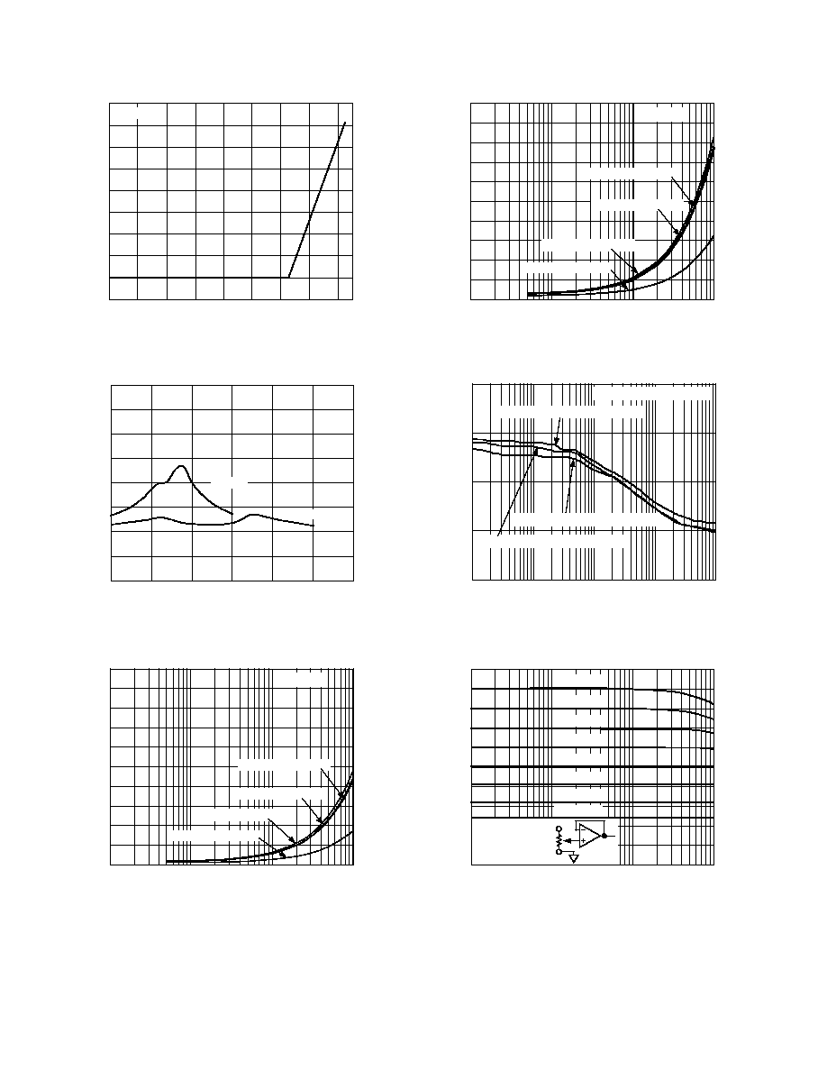
TPC 17. One Position Step Change at Half Scale
V
OUT
(50mV/DIV)
V
IN
(5mV/DIV)
TPC 18. Large Signal Settling Time

REV. 0
AD5207
≠8≠
V
W
(10mV/DIV)
TPC 19. Digital Feedthrough vs. Time
CODE ≠ Decimal
120
40
PO
TENTIOMETER MODE TEMPCO
≠
ppm/
C
0
100
80
60
40
20
0
≠20
32
64
96
128
160
192
224
256
TPC 20.
V
WB
/
T Potentiometer Mode
Temperature Coefficient
CODE ≠ Decimal
500
RHEOST
A
T MODE
TEMPCO
≠
ppm/
C
0
2500
2000
1500
1000
500
0
32
64
96
128
160
192
224
256
TPC 21.
R
WB
/
T Rheostat Mode Temperature Coefficient
CODE ≠ Decimal
100.0
10.0
0.1
0
32
THEORETICAL I
MAX
≠
mA
1.0
64
96
128
160
192
224
256
R
AB
= 10k
R
AB
= 50k
I
WB_MAX
TPC 22. I
MAX
vs. Code
REV. 0
AD5207
≠9≠
OPERATION
The AD5207 provides a dual channel, 256-position digitally
controlled variable resistor (VR) device. The terms VR, RDAC,
and digital potentiometer are sometimes used interchangeably.
Changing the programmable VR settings is accomplished by
clocking in a 10-bit serial data word into the SDI (Serial Data
Input) pin. The format of this data word is two address Bits, A1
and A0. With A1 and A2 are first and second bits respectively,
followed by eight data bits B7≠B0 with MSB first. Table I pro-
vides the serial register data word format. See Table III for the
AD5207 address assignments to decode the location of VR latch
receiving the serial register data in Bits B7 through B0. VR settings
can be changed one at a time in random sequence. The AD5207
presets to a midscale during power-on condition. AD5207 contains
a power shutdown
SHDN pin. When activated in logic low.
Terminals A on both RDACs will be open-circuited while the
wiper terminals W
X
are shorted to B
X
. As a result, a minimum
amount of leakage current will be consumed in both RDACs,
and the power dissipation is negligible. During the shutdown
mode, the VR latch settings are maintained. Thus the previ-
ous resistance values remain when the devices are resumed
from the shutdown.
DIGITAL INTERFACING
The AD5207 contains a standard three-wire serial input control
interface. The three inputs are clock (CLK), chip select (
CS),
and serial data input (SDI). The positive edge-sensitive CLK
input requires clean transitions to avoid clocking incorrect data
into the serial input register. Standard logic families work well.
If mechanical switches are used for product evaluation, they
should be debounced by a flip-flop or other suitable means. Fig-
ure 2 shows more detail of the internal digital circuitry. When
CS
is low, the clock loads data into the serial register on each posi-
tive clock edge; see Table II.
SER
REG
A0
D7
D6
D5
D4
D3
D2
D1
D0
ADDR
DEC
EN
RDAC
LATCH
#2
RDAC
LATCH
#1
AD5207
POWER-ON RESET
SHDN
V
DD
A1
W1
B1
A2
W2
B2
V
SS
CS
CLK
SDO
SDI
Figure 2. Block Diagram
The serial-data-output (SDO) pin contains an open drain
n-channel FET. This output requires a pull-up resistor in order
to transfer data to the next package's SDI pin. The pull-up
resistor termination voltage may be larger than the V
DD
supply
of the AD5207 SDO output device, e.g., the AD5207 could
operate at V
DD
= 3.3 V and the pull-up for interface to the next
device could be set at 5 V. This allows for daisy chaining several
RDACs from a single processor serial-data line. The clock period
may need to be increased when using a pull-up resistor to the
SDI pin of the following devices in series. Capacitive loading at
the daisy chain node SDO≠SDI between devices may add time
delay to subsequent devices. User should be aware of this poten-
tial problem in order to successfully achieve data transfer. See
Figure 3. When configuring devices for daisy-chaining, the
CS
should be kept low until all the bits of every package are clocked
into their respective serial registers, ensuring that the address bit
and data bits are in the proper decoding location. This requires
20 bits of address and data complying with the data word in
Table I if two AD5207 RDACs are daisy chained. During shut-
down
SHDN, the SDO output pin is forced to OFF (logic high
state) to disable power dissipation in the pull-up resistor. See
Figure 4 for equivalent SDO output circuit schematic.
R
P
2k
AD5207
SDO
SDI
CLK
CS
AD5207
SDO
SDI
CLK
CS
C
+V
Figure 3. Daisy-Chain Configuration Using SDO
Table II. Input Logic Control Truth Table
CLK
CS
SHDN
Register Activity
L
L
H
No SR effect, enables SDO pin.
P
L
H
Shift one bit in from the SDI pin. MSB
first. The tenth previously entered bit
is shifted out of the SDO pin.
X
P
H
Load SR data into RDAC latch based
on A0 decode (Table III).
X
H
H
No Operation.
X
H
L
Open circuits all resistor A Terminals,
connects W to B, turns off SDO out-
put transistor.
NOTE
P = positive edge, X = don't care, SR = shift register.
Table III. Address Decode Table
A1
A0
Latch Loaded
0
0
RDAC #1
0
1
RDAC #2

REV. 0
AD5207
≠10≠
The data setup and data hold times in the specification table
determine the data valid time requirements. The last ten bits of
the data word entered into the serial register are held when
CS
returns high and any extra bits are ignored. At the same time, when
CS goes high, it gates the address decoder enabling one of two
positive edge-triggered AD5207 RDAC latches; see Figure 5 detail.
SDI
CLK
CS
CK RS
D
Q
SERIAL
REGISTER
SDO
SHDN
INTERNAL
RS
Figure 4. Detail SDO Output Schematic of the AD5207
The target RDAC latch is loaded with the last eight bits of the
data word to complete one RDAC update. For AD5207, it
cannot update both channels simultaneously and therefore, two
separate 10-bit data words must be clocked in to change both
VR settings.
RDAC1
RDAC2
ADDR
DECODE
SERIAL
REGISTER
AD5207
SDI
CLK
CS
Figure 5. Equivalent Input Control Logic
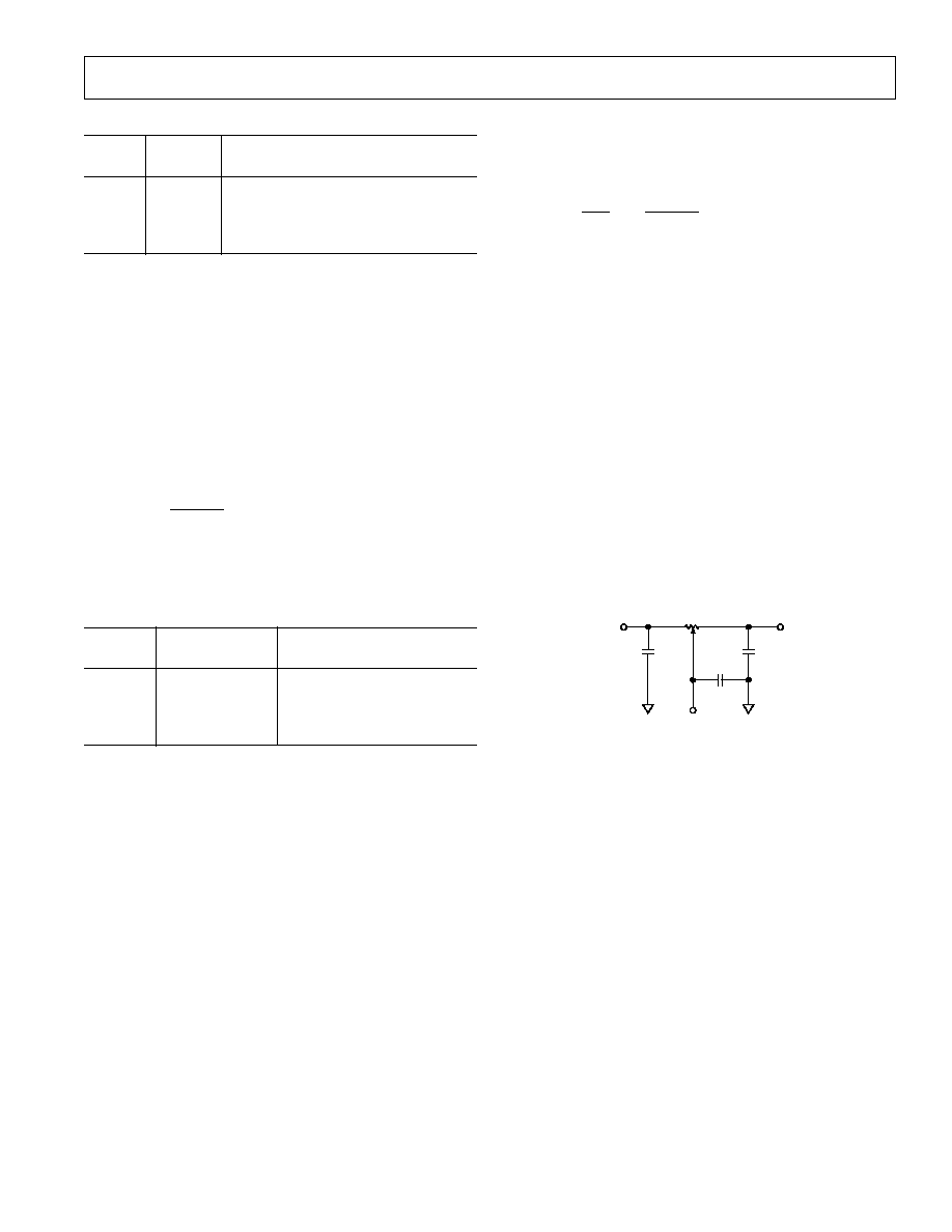
All digital inputs are protected with a series input resistor and
parallel Zener ESD structure shown in Figures 6 and 7. Applies
to digital input pins
CS, SDI, SDO, SHDN, and CLK. Digital
input level for Logic 1 can be anywhere from 2.4 V to 5 V
regardless of whether it is in single or dual supplies.
340
V
SS
LOGIC
DIGITAL PIN
Figure 6. ESD Protection of Digital Pins
A,B,W
V
SS
Figure 7. ESD Protection of Resistor Terminals
D7
D6
D5
D4
D3
D2
D1
D0
RDAC
LATCH
AND
DECODER
R
S
R
S
R
S
R
S
SHDN
Ax
Wx
Bx
Figure 8. Equivalent RDAC Circuit
PROGRAMMING THE VARIABLE RESISTOR
Rheostat Operation
The nominal resistance of the RDAC between Terminals A and
B is available with values of 10 k
, 50 k, and 100 k. The last
few digits of the part number determine the nominal resistance
value, e.g., 10 k
= 10; 50 k = 50; and 100 k = 100. The
nominal resistance (R
AB
) of the VR has 256 contact points
accessed by the wiper terminal, plus the B Terminal contact.
The 8-bit data in the RDAC latch is decoded to select one of
the 256 possible settings. Assume a 10 k
part is used, the
wiper's first connection starts at the B Terminal for data 00
H
.
Since there is a 45
wiper contact resistance, such connection
yields a minimum of 45
resistance between Terminals W and
B. The second connection is the first tap point corresponds to
84
(R
WB
= R
AB
/256 + R
W
= 39
+ 45 ) for data 01
H
. The
third connection is the next tap point representing 123
(39 ◊
2 + 45) for data 02
H
and so on. Each LSB value increase moves
the wiper up the resistor ladder until the last tap point is reached at
10006
(R
AB
≠ 1 LSB + R
W
). Figure 8 shows a simplified dia-
gram of the equivalent RDAC circuit.
The general equation determining the programmable output
resistance between W and B is:
R
D
D
R
R
WB
AB
W
( )
=
◊
+
256
(1)
where D is the data contained in the 8-bit RDAC latch, and R
AB
is the nominal end-to-end resistance.
For example, R
AB
=10 k
, A Terminal can be open-circuit or
tied to W. The following output resistance R
WB
will be set for
the following RDAC latch codes.
REV. 0
AD5207
≠11≠
Table IV.
D
R
WB
(DEC)
( )
Output State
255
10006
Full-Scale (R
AB
≠ 1 LSB + R
W
)
128
5045
Midscale
1
84
1 LSB
0
45
Zero-Scale (Wiper Contact Resistance)
Note that in the zero-scale condition a finite wiper resistance of
45
is present. Care should be taken to limit the current flow
between W and B in this state to a maximum current of no more
than 5 mA. Otherwise, degradation or possibly destruction of
the internal switch contacts can occur.
Similar to the mechanical potentiometer, the resistance of the
RDAC between the wiper W and Terminal A also produces a
digitally controlled resistance R
WA
. When these terminals are used,
the B Terminal should be let open or tied to the wiper terminal.
Setting the resistance value for R
WA
starts at a maximum value
of resistance and decreases as the data loaded in the latch is
increased in value. The general equation for this operation is:
R
D
D
R
R
WA
AB
W
( )
=
◊
+
256
256
≠
(2)
For example, when R
AB
= 10 k
, B terminal is either open or
tied to W, the following output resistance, R
WA
, will be set for
the following RDAC latch codes.
Table V.
D
R
WA
(DEC)
( )
Output State
255
84
Full-Scale (R
AB
/256 + R
W
)
128
5045
Midscale
1
10006
1 LSB
0
10045
Zero-Scale
The typical distribution of R
AB
from channel to channel matches
within
±1%. Device-to-device matching is process-lot depen-
dent and is possible to have
±30% variation. The change in R
AB
with temperature has a 500 ppm/
∞C temperature coefficient.
PROGRAMMING THE POTENTIOMETER DIVIDER
Voltage Output Operation
The digital potentiometer easily generates an output voltage
proportional to the input voltage. Let's ignore the effect of
the wiper resistance for the moment. For example, when con-
necting A Terminal to 5 V and B Terminal to ground, it produces
a programmable output voltage at the wiper starting at zero
volts up to 1 LSB less than 5 V. Each LSB of voltage is equal
to the voltage applied across terminal AB divided by the 256
position of the potentiometer divider. Since AD5207 is capable
for dual supplies, the general equation defining the output volt-
age with respect to ground for any given input voltage applied to
terminals AB is:
V
D
D
V
D
V
W
A
B
( )
=
+
-
256
256
256
(3)
Operation of the digital potentiometer in the divider mode
results in more accurate operation over temperature. Unlike the
rheostat mode, the output voltage is dependent on the ratio of
R
WA
and R
WB
and not the absolute values; therefore, the drift
reduces to 15 ppm/
∞C. There is no voltage polarity constraint
between Terminals A, B, and W as long as the terminal voltage
stays within V
SS
< V
TERM
< V
DD
.
RDAC CIRCUIT SIMULATION MODEL
The internal parasitic capacitances and the external capacitive
loads dominate the ac characteristics of the RDACs. Config-
ured as a potentiometer divider the ≠3 dB bandwidth of the
AD5207BRU10 (10 k
resistor) measures 600 kHz at half
scale. TPC 16 provides the large signal BODE plot characteris-
tics of the three available resistor versions 10 k
and 50 k.
The gain flatness versus frequency graph, TPC 16, predicts
filter applications performance. A parasitic simulation model has
been developed and is shown in Figure 9. Listing I provides a
macro model net list for the 10 k
RDAC:
C
W
70pF
C
B
C
A
B
A
RDAC
10k
W
C
B
= 45pF
C
A
= 45pF
Figure 9. RDAC Circuit Simulation Model for RDAC = 10 k
Listing I. Macro Model Net List for RDAC
.PARAM D=255, RDAC=10E3
*
.SUBCKT DPOT (A,W)
*
CA A 0 45E-12
RAW A W {(1-D/256)
*RDAC+50}
CW W 0 70E-12
RBW W B {D/256
*RDAC+50}
CB B 0 45E-12
*
.ENDS DPOT

REV. 0
AD5207
≠12≠
TEST CIRCUITS
Figures 10 to 18 define the test conditions used in product
Specification table.
V
MS
A
W
B
DUT
V+
V+
= V
DD
1 LSB = V+/2
N
Figure 10. Potentiometer Divider Nonlinearity Error Test
Circuit (INL, DNL)
V
MS
A
W
B
DUT
NO CONNECT
I
W
Figure 11. Resistor Position Nonlinearity Error (Rheostat
Operation; R-INL, R-DNL)
V
MS1
A
W
B
DUT
I
W
= V
DD
/R
NOMINAL
V
MS2
V
W
R
W
= [V
MS1
≠ V
MS2
]/I
W
Figure 12. Wiper Resistance Test Circuit
V
MS
%
V
DD
%
PSS (%/%) =
V+ = V
DD
10%
PSRR (dB) = 20 LOG
V
MS
V
DD
V
MS
A
W
B
V+
V
DD
V
A
Figure 13. Power Supply Sensitivity Test Circuit
(PSS, PSSR)
OP279
W
5V
B
V
OUT
OFFSET
GND
OFFSET BIAS
A
DUT
V
IN
Figure 14. Inverting Gain Test Circuit
OFFSET BIAS
B
OFFSET
GND
A
DUT
OP279
W
5V
V
OUT
V
IN
Figure 15. Noninverting Gain Test Circuit
OP42
V
OUT
V
IN
+15V
OFFSET
GND
≠15V
W
B
A
2.5V
DUT
Figure 16. Gain vs. Frequency Test Circuit
W
B
V
SS
TO V
DD
DUT
I
SW
CODE =
H
R
SW
=
0.1V
I
SW
0.1V
+
≠
Figure 17. Incremental ON Resistance Test Circuit
I
CM
A
W
B
NC
GND
NC
V
SS
V
DD
DUT
V
CM
NC = NO CONNECT
Figure 18. Common-Mode Leakage Current Test Circuit

REV. 0
AD5207
≠13≠
DIGITAL POTENTIOMETER FAMILY SELECTION GUIDE
Number
Resolution
Power
of VRs
Terminal
Interface
Nominal
(Number
Supply
Part
per
Voltage
Data
Resistance
of Wiper
Current
Number
Package
Range
Control
(k )
Positions)
(I
DD
)
Packages
Comments
AD5201
1
±3 V, +5.5 V
3-Wire
10, 50
33
40
µA
µSOIC-10
Full AC Specs, Dual Supply,
Pwr-On-Reset, Low Cost
AD5220
1
5.5 V
Up/Down
10, 50, 100
128
40
µA
PDIP, SO-8,
µSOIC-8 No Rollover, Pwr-On-Reset
AD7376
1
±15 V, +28 V
3-Wire
10, 50, 100, 1000
128
100
µA
PDIP-14, SOL-16,
Single +28 V or Dual
±15 V
TSSOP-14
Supply Operation
AD5200
1
±3 V, +5.5 V
3-Wire
10, 50
256
40
µA
µSOIC-10
Full AC Specs, Dual Supply,
Pwr-On-Reset
AD8400
1
5.5 V
3-Wire
1, 10, 50, 100
256
5
µA
SO-8
Full AC Specs
AD5260
1
±5 V, +15 V
3-Wire
20, 50, 200
256
60
µA
TSSOP-14
15 V or
±5 V,
TC < 50 ppm/
∞C
AD5241
1
±3 V, +5.5 V
2-Wire
10, 100, 1000
256
50
µA
SO-14, TSSOP-14
I
2
C-Compatible, TC
< 50 ppm/
∞C
AD5231
* 1
±3 V, +5.5 V
3-Wire
10, 50, 100
1024
20
µA
TSSOP-16
Nonvolatile Memory, Direct
Program, I/D,
±6 dB Settability
AD5222
2
±3 V, +5.5 V
Up/Down
10, 50, 100, 1000
128
80
µA
SO-14, TSSOP-14
No Rollover, Stereo, Pwr-On-
Reset, TC < 50 ppm/
∞C
AD8402
2
5.5 V
3-Wire
1, 10, 50, 100
256
5
µA
PDIP, SO-14,
Full AC Specs, nA
TSSOP-14
Shutdown Current
AD5207
2
±3 V, +5.5 V
3-Wire
10, 50, 100
256
40
µA
TSSOP-14
Full AC specs, Dual Supply,
Pwr-On-Reset, SDO
AD5232
* 2
±3 V, +5.5 V
3-Wire
10, 50, 100
256
20
µA
TSSOP-16
Nonvolatile Memory, Direct
Program, I/D,
±6 dB Settability
AD5235
* 2
±3 V, +5.5 V
3-Wire
25, 250
1024
20
µA
TSSOP-16
Nonvolatile Memory, Direct
Program, TC < 50 ppm/
∞C
AD5242
2
±3 V, +5.5 V
2-Wire
10, 100, 1000
256
50
µA
SO-16, TSSOP-16
I
2
C-Compatible, TC
< 50 ppm/
∞C
AD5262
* 2
±5 V, +15 V
3-Wire
20, 50, 200
256
60
µA
TSSOP-16
±15 V or ±5 V, Pwr-On-
Reset, TC < 50 ppm/
∞C
AD5203
4
5.5 V
3-Wire
10, 100
64
5
µA
PDIP, SOL-24,
Full AC Specs, nA
TSSOP-24
Shutdown Current
AD5233
* 4
±3 V, +5.5 V
3-Wire
10, 50, 100
64
20
µA
TSSOP-16
Nonvolatile Memory, Direct
Program, I/D,
±6 dB Settability
AD5204
4
±3 V, +5.5 V
3-Wire
10, 50, 100
256
60
µA
PDIP, SOL-24,
Full AC Specs, Dual Supply,
TSSOP-24
Pwr-On-Reset
AD8403
4
5.5 V
3-Wire
1, 10, 50, 100
256
5
µA
PDIP, SOL-24,
Full AC Specs, nA
TSSOP-24
Shutdown Current
AD5206
6
±3 V, +5.5 V
3-Wire
10, 50, 100
256
60
µA
PDIP, SOL-24,
Full AC Specs, Dual Supply,
TSSOP-24
Pwr-On-Reset
*Future product, consult factory for latest status.
Latest Digital Potentiometer Information available at
www.analog.com/support/standard_linear/selection_guides/dig_pot.html
REV. 0
AD5207
≠14≠
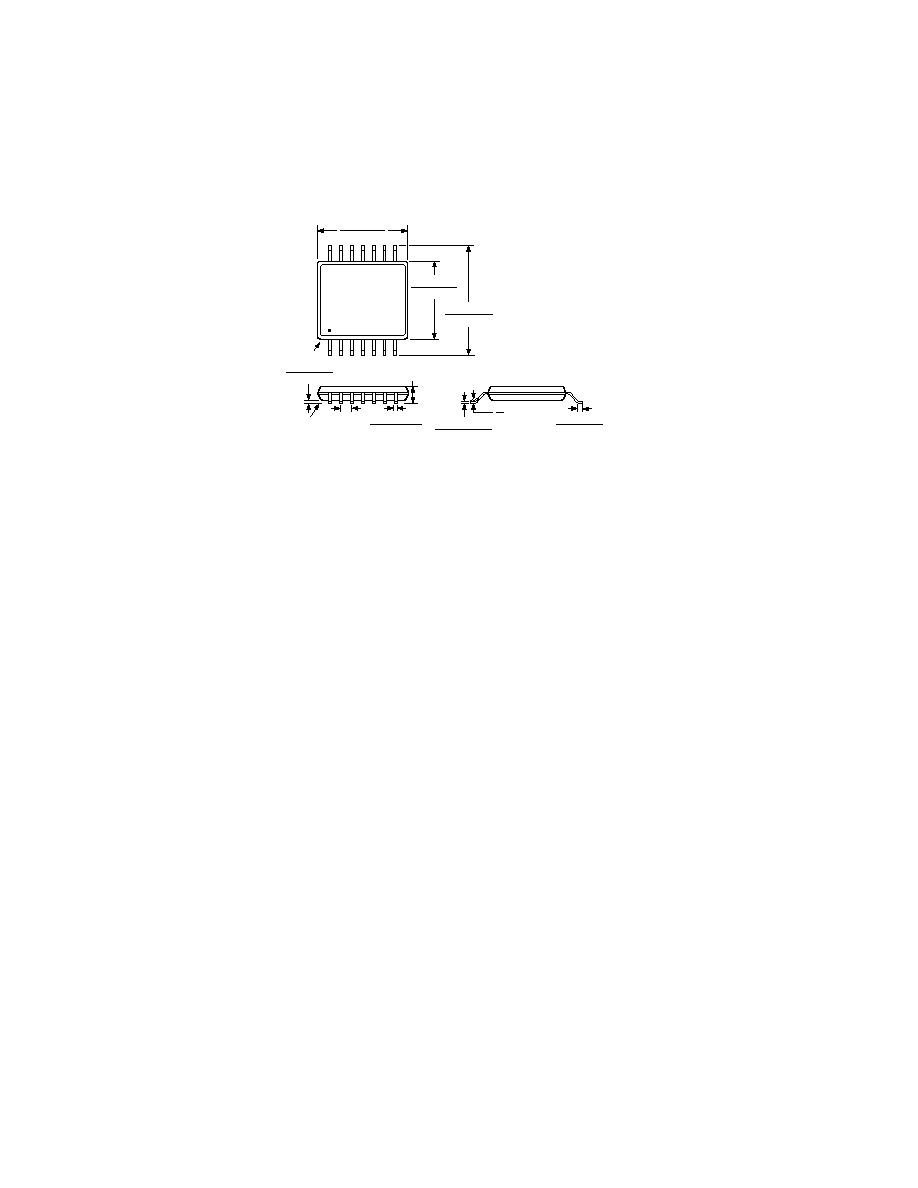
OUTLINE DIMENSIONS
Dimensions shown in inches and (mm)
14-Lead TSSOP
(RU-14)
14
8
7
1
0.256 (6.50)
0.246 (6.25)
0.177 (4.50)
0.169 (4.30)
PIN 1
0.201 (5.10)
0.193 (4.90)
SEATING
PLANE
0.006 (0.15)
0.002 (0.05)
0.0118 (0.30)
0.0075 (0.19)
0.0256
(0.65)
BSC
0.0433 (1.10)
MAX
0.0079 (0.20)
0.0035 (0.090)
0.028 (0.70)
0.020 (0.50)
8
0

≠15≠

≠16≠
C01885≠1.5≠4/01(0)
PRINTED IN U.S.A.