 | –≠–ª–µ–∫—Ç—Ä–æ–Ω–Ω—ã–π –∫–æ–º–ø–æ–Ω–µ–Ω—Ç: AD741LH | –°–∫–∞—á–∞—Ç—å:  PDF PDF  ZIP ZIP |

REV. A
Information furnished by Analog Devices is believed to be accurate and
reliable. However, no responsibility is assumed by Analog Devices for its
use, nor for any infringements of patents or other rights of third parties
which may result from its use. No license is granted by implication or
otherwise under any patent or patent rights of Analog Devices.
a
AD741 Series
One Technology Way, P.O. Box 9106, Norwood, MA 02062-9106, U.S.A.
Tel: 617/329-4700
World Wide Web Site: http://www.analog.com
Fax: 617/326-8703
© Analog Devices, Inc., 1997
Low Cost,
High Accuracy IC Op Amps
CONNECTION DIAGRAMS
TO-99 (H) Package
NC = NO CONNECT
Mini-DIP (N) Package
NC = NO CONNECT
GENERAL DESCRIPTION
The Analog Devices AD741 Series are high performance mono-
lithic operational amplifiers. All the devices feature full short
circuit protection and internal compensation.
The Analog Devices AD741J, AD741K, AD741L, and AD741S
are specially tested and selected versions of the standard AD741
operational amplifier. Improved processing and additional elec-
trical testing guarantee the user precision performance at a very
low cost. The AD741J, K and L substantially increase overall
accuracy over the standard AD741C by providing maximum
limits on offset voltage drift and significantly reducing the errors
due to offset voltage, bias current, offset current, voltage gain,
power supply rejection and common-mode rejection. For example,
the AD741L features maximum offset voltage drift of 5
µ
V/
∞
C,
offset voltage of 0.5 mV max, offset current of 5 nA max, bias
current of 50 nA max and a CMRR of 90 dB min. The AD741S
offers guaranteed performance over the extended temperature
range of ≠55
∞
C to +125
∞
C, with max offset voltage drift of
15
µ
V/
∞
C, max offset voltage of 4 mV, max offset current of
25 nA, and a minimum CMRR of 80 dB.
FEATURES
Precision Input Characteristics
Low V
OS
: 0.5 mV max (L)
Low V
OS
Drift: 5 V/ C max (L)
Low I
b
: 50 nA max (L)
Low l
OS
: 5 nA max (L)
High CMRR: 90 dB min (K, L)
High Output Capability
A
OL
= 25,000 min, 1 k Load (J, S) T
MIN
to T
MAX
V
O
= 10 V min, 1 k Load (J, S)
Chips and MIL-STD-883B Parts Available
HIGH OUTPUT CAPABILITY
Both the AD741J and AD741S offer the user the additional
advantages of high guaranteed output current and gain at low
values of load impedance. The AD741J guarantees a minimum
gain of 25,000 swinging
±
10 V into a 1 k
load from 0
∞
C to
+70
∞
C. The AD741S guarantees a minimum gain of 25,000
swinging
±
10 V into a 1 k
load from ≠55
∞
C to +125
∞
C.
All devices feature full short circuit protection, high gain, high
common-mode range and internal compensation. The AD741J,
K and L are specified for operation from 0 to +70
∞
C and are
available in both the TO-99 and mini-DIP packages. The
AD741S is specified for operation from ≠55
∞
C to +125
∞
C, and
is available in the TO-99 package.

≠2≠
REV. A
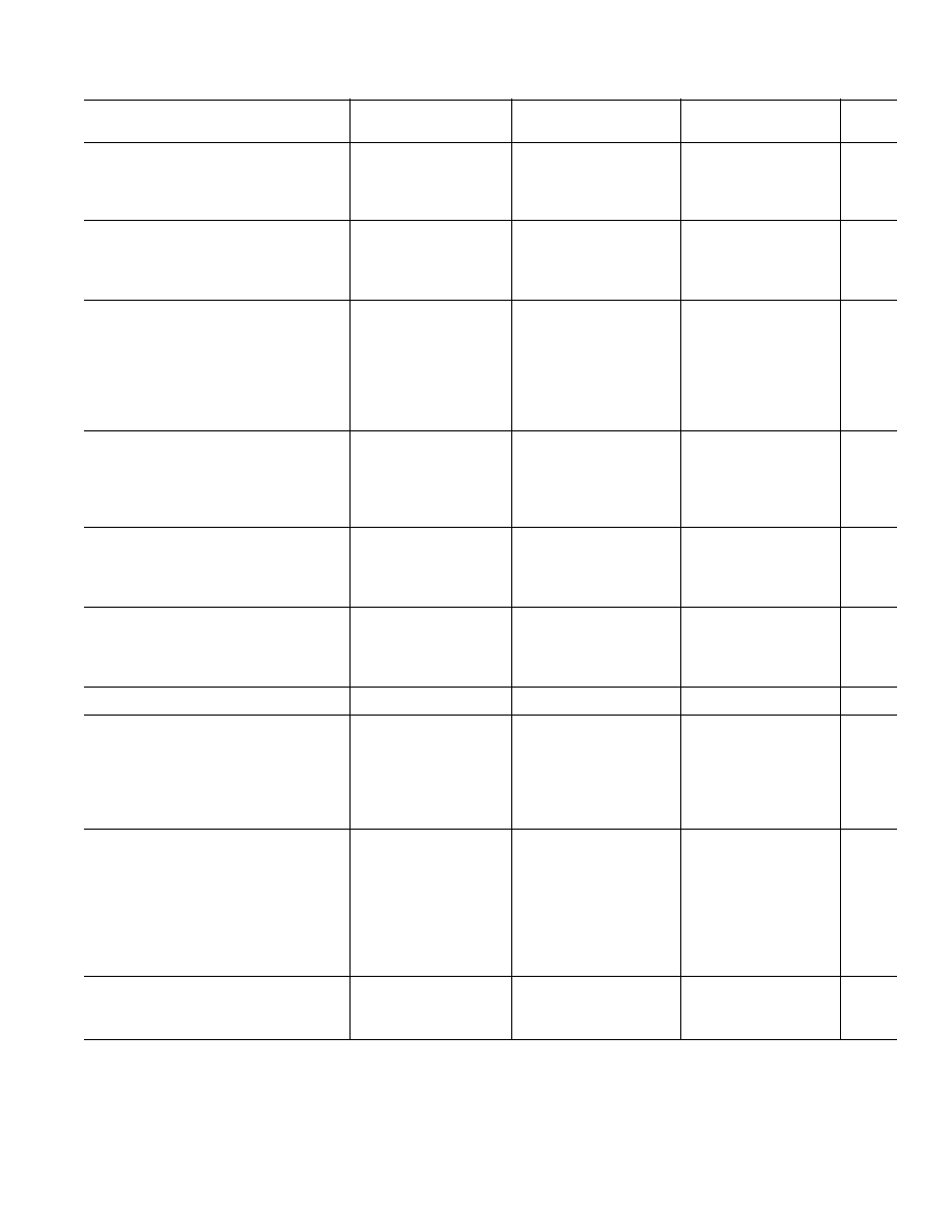
AD741 Series≠SPECIFICATIONS
AD741C
AD741
AD741J
Model
Min
Typ
Max
Min
Typ
Max
Min
Typ
Max
Units
OPEN-LOOP GAIN
R
L
= 1 k
, V
O
=
±
10 V
50,000
200,000
V/V
R
L
= 2 k
, V
O
=
±
10 V
20,000
200,000
50,000
200,000
V/V
T
A
= min to max R
L
= 2 k
15,000
25,000
25,000
V/V
OUTPUT CHARACTERISTICS
Voltage @ R
L
= 1 k
, T
A
= min to max
10
±
13
V
Voltage @ R
L
= 2 k
, T
A
= min to max
10
±
13
10
±
13
V
Short Circuit Current
25
25
25
mA
FREQUENCY RESPONSE
Unity Gain, Small Signal
1
1
1
MHz
Full Power Response
10
10
10
kHz
Slew Rate
0.5
0.5
0.5
V/
µ
s
Transient Response (Unity Gain)
Rise Time C
L
10 V p-p
0.3
0.3
0.3
µ
s
Overshoot
5.0
5.0
5.0
%
INPUT OFFSET VOLTAGE
Initial, R
S
10 k
, Adjust to Zero
1.0
6.0
1.0
5.0
1.0
3.0
mV
T
A
= min to max
1.0
7.5
1.0
6.0
4.0
mV
Average vs. Temperature (Untrimmed)
20
µ
V/
∞
C
vs. Supply, T
A
= min to max
30
100
µ
V/V
INPUT OFFSET CURRENT
Initial
20
200
20
200
5
50
nA
T
A
= min to max
40
300
85
500
100
nA
Average vs. Temperature
0.1
nA/
∞
C
INPUT BIAS CURRENT
Initial
80
500
80
500
40
200
nA
T
A
= min to max
120
800
300
1,500
400
nA
Average vs. Temperature
0.6
nA/
∞
C
INPUT IMPEDANCE DIFFERENTIAL 0.3
2.0
0.3
2.0
1.0
M
INPUT VOLTAGE RANGE
1
Differential, max Safe
±
30
V
Common-Mode, max Safe
±
12
±
13
±
12
±
13
±
15
V
Common-Mode Rejection,
R
S
=
10 k
, T
A
= min to max,
V
IN
=
±
12 V
70
90
70
90
80
90
dB
POWER SUPPLY
Rated Performance
±
15
±
15
±
15
V
Operating
±
5
±
18
V
Power Supply Rejection Ratio
30
150
30
150
µ
V/V
Quiescent Current
1.7
2.8
1.7
2.8
2.2
3.3
mA
Power Consumption
50
85
50
85
50
85
mW
T
A
= min
60
100
mW
T
A
= max
45
75
mW
TEMPERATURE RANGE
Operating Rated Performance
0
+70
≠55
+125
0
+70
∞
C
Storage
≠65
+150
≠65
+150
≠65
+150
∞
C
NOTES
1
For supply voltages less than
±
15 V, the absolute maximum input voltage is equal to the supply voltage.
All min and max specifications are guaranteed. Specifications shown in boldface are tested on all production units at final electrical test. Results from those tests are
used to calculate outgoing quality levels.
Specifications subject to change without notice.
(typical @ +25 C and 15 V dc, unless otherwise noted)
≠3≠
REV. A
AD741 Series
AD741K
AD741L
AD741S
Model
Min
Typ
Max
Min
Typ
Max
Min
Typ
Max
Units
OPEN-LOOP GAIN
R
L
= 1 k
, V
O
=
±
10 V
50,000
200,000
V/V
R
L
= 2 k
, V
O
=
±
10 V
50,000
200,000
50,000
200,000
V/V
T
A
= min to max R
L
= 2 k
25,000
25,000
25,000
V/V
OUTPUT CHARACTERISTICS
Voltage @ R
L
= 1 k
, T
A
= min to max
V
Voltage @ R
L
= 2 k
, T
A
= min to max
10
±
13
10
±
13
10
±
13
V
Short Circuit Current
25
25
25
mA
FREQUENCY RESPONSE
Unity Gain, Small Signal
1
1
1
MHz
Full Power Response
10
10
10
kHz
Slew Rate
0.5
0.5
0.5
V/
µ
s
Transient Response (Unity Gain)
Rise Time
0.3
0.3
0.3
µ
s
Overshoot
5.0
5.0
5.0
%
INPUT OFFSET VOLTAGE
Initial, R
S
10 k
, Adjust to Zero
0.5
2.0
0.2
0.5
1.0
2
mV
T
A
= min to max
3.0
1.0
4
mV
Average vs. Temperature (Untrimmed)
6.0
15.0
2.0
5.0
6.0
15
µ
V/
∞
C
vs. Supply, T
A
= min to max
5
15.0
5
15.0
30
100
µ
V/V
INPUT OFFSET CURRENT
Initial
2
10
2
5
2
10
nA
T
A
= min to max
15
10
25
nA
Average vs. Temperature
0.02
0.02
0.02
0.1
0.1
0.25
nA/
∞
C
INPUT BIAS CURRENT
Initial
30
75
30
50
30
75
nA
T
A
= min to max
120
100
250
nA
Average vs. Temperature
0.6
1.5
0.6
1.0
0.6
2.0
nA/
∞
C
INPUT IMPEDANCE DIFFERENTIAL
2.0
2.0
2.0
M
INPUT VOLTAGE RANGE
1
Differential, max Safe
±
30
±
30
±
30
V
Common-Mode, max Safe
±
15
±
15
±
15
V
Common-Mode Rejection,
R
S
=
10 k
, T
A
= min to max,
V
IN
=
±
12 V
90
100
90
100
90
100
dB
POWER SUPPLY
Rated Performance
±
15
±
15
±
15
V
Operating
±
5
±
22
±
5
±
22
±
5
±
22
V
Power Supply Rejection Ratio
20
20
20
µ
V/V
Quiescent Current
1.7
2.8
1.7
2.8
2.0
2.8
mA
Power Consumption
50
85
50
85
50
85
mW
T
A
= min
60
100
mW
T
A
= max
75
115
mW
TEMPERATURE RANGE
Operating Rated Performance
0
+70
0
+70
≠55
+125
∞
C
Storage
≠65
+150
≠65
+150
≠65
+150
∞
C
AD741 Series
≠4≠
REV. A
ABSOLUTE MAXIMUM RATINGS
AD741, J,
Absolute Maximum Ratings
K, L, S
AD741C
Supply Voltage
±
22 V
±
18 V
Internal Power Dissipation
500 mW
1
500 mW
Differential Input Voltage
±
30 V
±
30 V
Input Voltage
±
15 V
±
15 V
Storage Temperature Range
≠65
∞
C
≠65
∞
C
to +150
∞
C
to +150
∞
C
Lead Temperature
(Soldering, 60 sec)
+300
∞
C
+300
∞
C
Output Short Circuit Duration
Indefinite
2
Indefinite
NOTES
1
Rating applies for case temperature to +125
∞
C. Derate TO-99 linearity at
6.5 mW/
∞
C for ambient temperatures above +70
∞
C.
2
Rating applies for shorts to ground or either supply at case temperatures to
+125
∞
C or ambient temperatures to +75
∞
C.
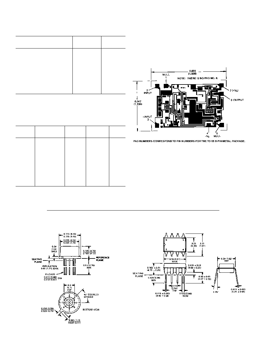
ORDERING GUIDE
Temperature
Initial Off
Package
Package
Model
1
Range
Set Voltage Description Option
AD741CN 0
∞
C to +70
∞
C
6.0 mV
Mini-DIP
(N-8)
AD741CH 0
∞
C to +70
∞
C
6.0 mV
TO-99
(H-08A)
AD741JN
0
∞
C to +70
∞
C
3.0 mV
Mini-DIP
(N-8)
AD741JH
0
∞
C to +70
∞
C
3.0 mV
TO-99
(H-08A)
AD741KN 0
∞
C to +70
∞
C
2.0 mV
Mini-DIP
(N-8)
AD741KH 0
∞
C to +70
∞
C
2.0 mV
TO-99
(H-08A)
AD741LN 0
∞
C to +70
∞
C
0.5 mV
Mini-DIP
(N-8)
AD741LH 0
∞
C to +70
∞
C
0.5 mV
TO-99
(H-08A)
AD741H
≠55
∞
C to +125
∞
C 5.0 mV
TO-99
(H-08A)
AD741SH ≠55
∞
C to +125
∞
C 2.0 mV
TO-99
(H-08A)
NOTE
1
J, K and S grade chips also available.
METALIZATION PHOTOGRAPH
All versions of the AD741 are available in chip form.
Contact factory for latest dimensions.
Dimensions shown in inches and (mm).
OUTLINE DIMENSIONS
Dimensions shown in inches and (mm).
TO-99 (H)
Mini DIP (N)

AD741 Series≠Typical Performance Curves
≠5≠
REV. A
Figure 1. Input Bias Current vs. Temperature
Figure 2. Input Offset Current vs. Temperature
Figure 3. Open-Loop Gain vs. Frequency
Figure 4. Open-Loop Phase Response vs. Frequency
Figure 5. Common-Mode Rejection vs. Frequency
Figure 6. Broad Band Noise vs. Source Resistance

AD741 Series
≠6≠
REV. A
C687b≠0≠5/97
PRINTED IN U.S.A.
Figure 7. Input Noise Voltage vs. Frequency
Figure 8. Input Noise Current vs. Frequency
Figure 9. Voltage Follower Large Signal Pulse Response
Figure 10. Output Voltage Swing vs. Supply Voltage
Figure 11. Output Voltage Swing vs. Load Resistance
Figure 12. Output Voltage Swing vs. Frequency