 | ÐлекÑÑоннÑй компоненÑ: AD745 | СкаÑаÑÑ:  PDF PDF  ZIP ZIP |
Äîêóìåíòàöèÿ è îïèñàíèÿ www.docs.chipfind.ru
REV. D
Information furnished by Analog Devices is believed to be accurate and
reliable. However, no responsibility is assumed by Analog Devices for its
use, nor for any infringements of patents or other rights of third parties that
may result from its use. No license is granted by implication or otherwise
under any patent or patent rights of Analog Devices.
a
AD745
One Technology Way, P.O. Box 9106, Norwood, MA 02062-9106, U.S.A.
Tel: 781/329-4700
www.analog.com
Fax: 781/326-8703
© Analog Devices, Inc., 2002
Ultralow Noise,
High Speed, BiFET Op Amp
CONNECTION DIAGRAM
FEATURES
ULTRALOW NOISE PERFORMANCE
2.9 nV/ Hz at 10 kHz
0.38 V p-p, 0.1 Hz to 10 Hz
6.9 fA/ Hz Current Noise at 1 kHz
EXCELLENT AC PERFORMANCE
12.5 V/ s Slew Rate
20 MHz Gain Bandwidth Product
THD = 0.0002% @ 1 kHz
Internally Compensated for Gains of +5 (or 4) or
Greater
EXCELLENT DC PERFORMANCE
0.5 mV Max Offset Voltage
250 pA Max Input Bias Current
2000 V/mV Min Open Loop Gain
Available in Tape and Reel in Accordance with
EIA-481A Standard
APPLICATIONS
Sonar
Photodiode and IR Detector Amplifiers
Accelerometers
Low Noise Preamplifiers
High Performance Audio
PRODUCT DESCRIPTION
The AD745 is an ultralow noise, high-speed, FET input opera-
tional amplifier. It offers both the ultralow voltage noise and
high speed generally associated with bipolar input op amps and
the very low input currents of FET input devices. Its 20 MHz
bandwidth and 12.5 V/
µs slew rate makes the AD745 an ideal
SOURCE RESISTANCE
1000
100
INPUT NOISE
V
O
L
T
A
GE nV/ Hz
100
10
1
1k
10k
100k
1M
10M
R
SOURCE
R
SOURCE
E
O
OP37 AND
RESISTOR
AD745 AND
RESISTOR
AD745 AND RESISTOR
OR
OP37 AND RESISTOR
RESISTOR NOISE ONLY
Figure 1.
amplifier for high-speed applications demanding low noise and
high dc precision. Furthermore, the AD745 does not exhibit an
output phase reversal.
The AD745 also has excellent dc performance with 250 pA
maximum input bias current and 0.5 mV maximum offset voltage.
The internal compensation of the AD745 is optimized for higher
gains, providing a much higher bandwidth and a faster slew
rate. This makes the AD745 especially useful as a preamplifier
where low level signals require an amplifier that provides both
high amplification and wide bandwidth at these higher gains.
The AD745 is available in two performance grades. The AD745J
and AD745K are rated over the commercial temperature range
of 0
°C to 70°C, and are available in the 16-lead SOIC package.
FREQUENCY Hz
120
100
OPEN-LOOP GAIN
dB
100
80
60
40
20
0
20
1k
10k
100k
1M
10M
100M
120
100
80
60
40
20
0
20
PHASE MARGIN
Degrees
GAIN
PHASE
Figure 2.
16-Lead SOIC (R) Package
REV. D
2
AD745SPECIFICATIONS
(@ +25 C and 15 V dc, unless otherwise noted.)
Model
AD745J
AD745K
Conditions
Min
Typ
Max
Min
Typ
Max
Unit
INPUT OFFSET VOLTAGE
1
Initial Offset
0.25
1.0
0.1
0.5
mV
Initial Offset
T
MIN
to T
MAX
1.5
1.0
mV
vs. Temp.
T
MIN
to T
MAX
2
2
µV/°C
vs. Supply (PSRR)
12 V to 18 V
2
90
96
100
106
dB
vs. Supply (PSRR)
T
MIN
to T
MAX
88
98
105
dB
INPUT BIAS CURRENT
3
Either Input
V
CM
= 0 V
150
400
150
250
pA
Either Input
@ T
MAX
V
CM
= 0 V
8.8
5.5
nA
Either Input
V
CM
= +10 V
250
600
250
400
pA
Either Input, V
S
=
±5 V
V
CM
= 0 V
30
200
30
125
pA
INPUT OFFSET CURRENT
V
CM
= 0 V
40
150
30
75
pA
Offset Current
@ T
MAX
V
CM
= 0 V
2.2
1.1
nA
FREQUENCY RESPONSE
Gain BW, Small Signal
G = 4
20
20
MHz
Full Power Response
V
O
= 20 V p-p
120
120
kHz
Slew Rate
G = 4
12.5
12.5
V/
µs
Settling Time to 0.01%
5
5
µs
Total Harmonic
f = 1 kHz
Distortion
4
G = 4
0.0002
0.0002
%
INPUT IMPEDANCE
Differential
1
× 10
10
20
1
× 10
10
20
pF
Common Mode
3
× 10
11
18
3
× 10
11
18
pF
INPUT VOLTAGE RANGE
Differential
5
±20
± 20
V
Common-Mode Voltage
+13.3, 10.7
+13.3, 10.7
V
Over Max Operating Range
6
10
+12
10
+12
V
Common-Mode
Rejection Ratio
V
CM
=
± 10 V
80
95
90
102
dB
T
MIN
to T
MAX
78
88
dB
INPUT VOLTAGE NOISE
0.1 to 10 Hz
0.38
0.38
1.0
µV p-p
f = 10 Hz
5.5
5.5
10.0
nV/
Hz
f = 100 Hz
3.6
3.6
6.0
nV/
Hz
f = 1 kHz
3.2
5.0
3.2
5.0
nV/
Hz
f = 10 kHz
2.9
4.0
2.9
4.0
nV/
Hz
INPUT CURRENT NOISE
f = 1 kHz
6.9
6.9
fA/
Hz
OPEN LOOP GAIN
V
O
=
±10 V
R
LOAD
2 k
1000
4000
2000
4000
V/mV
T
MIN
to T
MAX
800
1800
V/mV
R
LOAD
= 600
1200
1200
V/mV
OUTPUT CHARACTERISTICS
Voltage
R
LOAD
600
+13, 12
+13, 12
V
R
LOAD
600
+13.6, 12.6
+13.6, 12.6
V
T
MIN
to T
MAX
+12, 10
+12, 10
V
R
LOAD
2 k
±12
+13.8, 13.1
+13.8, 13.1
V
Current
Short Circuit
20
40
20
40
mA
POWER SUPPLY
Rated Performance
±15
± 15
V
Operating Range
±4.8
± 18
± 4.8
± 18
V
Quiescent Current
8
10.0
8
10.0
mA
TRANSISTOR COUNT
# of Transistors
50
50
NOTES
1
Input offset voltage specifications are guaranteed after five minutes of operations at T
A
= 25
°C.
2
Test conditions: +V
S
= 15 V, V
S
= 12 V to 18 V and +V
S
= 12 V to +18 V, V
S
= 15 V.
3
Bias current specifications are guaranteed maximum at either input after five minutes of operation at T
A
= 25
°C. For higher temperature, the current doubles every 10°C.
4
Gain = 4, R
L
= 2 k
, C
L
= 10 pF.
5
Defined as voltage between inputs, such that neither exceeds
± 10 V from common.
6
The AD745 does not exhibit an output phase reversal when the negative common-mode limit is exceeded.
All min and max specifications are guaranteed.
Specifications subject to change without notice.
AD745 ELECTRICAL CHARACTERISTICS
REV. D
AD745
3
CAUTION
ESD (electrostatic discharge) sensitive device. Electrostatic charges as high as 4000 V readily
accumulate on the human body and test equipment and can discharge without detection. Although
the AD745 features proprietary ESD protection circuitry, permanent damage may occur on devices
subjected to high-energy electrostatic discharges. Therefore, proper ESD precautions are
recommended to avoid performance degradation or loss of functionality.
WARNING!
ESD SENSITIVE DEVICE
ORDERING GUIDE
Package
Model
Temperature Range
Option
*
AD745JR-16
0
°C to 70°C
R-16
AD745KR-16
0
°C to 70°C
R-16
*
R = Small Outline IC.
ABSOLUTE MAXIMUM RATINGS
1
Supply Voltage . . . . . . . . . . . . . . . . . . . . . . . . . . . . . . . .
±18 V
Internal Power Dissipation
2
SOIC Package . . . . . . . . . . . . . . . . . . . . . . . . . . . . . . 1.2 W
Input Voltage . . . . . . . . . . . . . . . . . . . . . . . . . . . . . . . . . . .
±V
S
Output Short-Circuit Duration . . . . . . . . . . . . . . . . Indefinite
Differential Input Voltage . . . . . . . . . . . . . . . . . . +V
S
and V
S
Storage Temperature Range (R) . . . . . . . . . 65
°C to +125°C
Operating Temperature Range
AD745J/K . . . . . . . . . . . . . . . . . . . . . . . . . . . . 0
°C to 70°C
Lead Temperature Range (Soldering 60 sec) . . . . . . . . . 300
°C
NOTES
1
Stresses above those listed under Absolute Maximum Ratings may cause perma-
nent damage to the device. This is a stress rating only; functional operation of the
device at these or any other conditions above those indicated in the operational
section of this specification is not implied. Exposure to Absolute Maximum Rating
conditions for extended periods may affect device reliability.
2
16-Pin Plastic SOIC Package:
JA
= 100
°C/W,
JC
= 30
°C/W
ESD SUSCEPTIBILITY
An ESD classification per method 3015.6 of MIL-STD-883C
has been performed on the AD745, which is a class 1 device.
Using an IMCS 5000 automated ESD tester, the two null pins
will pass at voltages up to 1,000 volts, while all other pins will
pass at voltages exceeding 2,500 volts.
REV. D
AD745
4
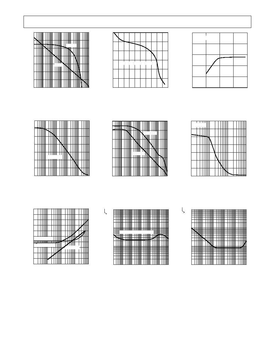
Typical Performance Characteristics
(@ + 25 C, V
S
= 15 V, unless otherwise noted.)
SUPPLY VOLTAGE
VOLTS
INPUT V
O
L
T
A
GE
SWING
V
20
0
15
10
5
0
5
10
15
20
R
LOAD
= 10k
+V
IN
V
IN
TPC 1. Input Voltage Swing vs.
Supply Voltage
SUPPLY VOLTAGE
VOLTS
Q
UIESCENT CURRENT
mA
12
0
9
6
3
0
5
10
15
20
TPC 4. Quiescent Current vs.
Supply Voltage
COMMON-MODE VOLTAGE V
INPUT BIAS CURRENT
pA
300
12
200
100
0
9
6
3
0
3
6
9
12
TPC 7. Input Bias Current vs.
Common-Mode Voltage
LOAD RESISTANCE
OUTPUT V
O
L
T
A
GE
SWING
V
p-p
35
10
30
25
20
15
10
5
0
100
1k
10k
TPC 3. Output Voltage Swing vs.
Load Resistance
FREQUENCY Hz
OUTPUT IMPED
ANCE
200
10k
100
10
1
0.1
0.01
100k
1M
10M
100M
CLOSED LOOP GAIN = 5
TPC 6. Output Impedance vs.
Frequency
TEMPERATURE C
GAIN B
AND
WIDTH PR
ODUCT
MHz
28
60
26
24
22
20
18
16
40 20
0
20
40 60
80 100 120 140
14
TPC 9. Gain Bandwidth Product vs.
Temperature
SUPPLY VOLTAGE
VOLTS
INPUT V
O
L
T
A
GE
SWING
V
20
0
15
10
5
0
5
10
15
20
R
LOAD
= 10k
POSITIVE
SUPPLY
NEGATIVE
SUPPLY
TPC 2. Output Voltage Swing vs.
Supply Voltage
TEMPERATURE C
INPUT BIAS CURRENT
Amps
10
6
60
10
7
10
8
10
9
10
10
10
11
10
12
40 20
0
20
40 60
80 100 120 140
TPC 5. Input Bias Current vs.
Temperature
TEMPERATURE C
INPUT BIAS CURRENT
Amps
10
6
60
10
7
10
8
10
9
10
10
10
11
10
12
40 20
0
20
40 60
80 100 120 140
TPC 8. Short Circuit Current Limit vs.
Temperature
REV. D
5
AD745
FREQUENCY Hz
OPEN-LOOP GAIN
dB
120
20
100
100
80
60
20
0
40
1k
10k
100k
1M
10M
100M
GAIN
PHASE
TPC 10. Open-Loop Gain and Phase
vs. Frequency
FREQUENCY Hz
COMMON-MODE REJECTION
dB
120
50
100
110
100
90
70
60
80
1k
10k
100k
1M
10M
V
cm
= 10V
TPC 13. Common-Mode Rejection vs.
Frequency
FREQUENCY Hz
T
O
T
A
L HARMONIC DIST
O
R
T
ION (THD)
dB
40
140
10
100
100k
1k
10k
100
120
60
80
1.0
0.1
0.01
0.001
0.0001
0.00001
T
O
T
A
L HARMONIC DIST
O
R
T
ION (THD)
%
GAIN = +10
GAIN = +100
GAIN = 4
TPC 16. Total Harmonic Distortion
vs. Frequency
TEMPERATURE C
SLEW RA
TE
V/
s
14
8
60
12
10
40 20 0
20
40 60
80 100 110 120
CLOSED-LOOP GAIN = 5
TPC 11. Slew Rate vs. Temperature
FREQUENCY Hz
PO
WER SUPPL
Y REJECTION
dB
120
100
100
80
60
20
0
40
1k
10k
100k
1M
10M
100M
+SUPPLY
SUPPLY
TPC 14. Power Supply Rejection
vs. Frequency
FREQUENCY Hz
NOISE
V
O
L
T
A
GE (ref
e
rred to input)
nV/ Hz
100
10
10
0.1
1.0
100
1k
10k
100k
1M
10M
CLOSED-LOOP GAIN = 5
TPC 17. Input Noise Voltage
Spectral Density
SUPPLY VOLTAGE
VOLTS
OPEN-LOOP GAIN
dB
150
140
80
0
5
20
10
15
130
120
100
R
L
= 2k
TPC 12. Open-Loop Gain vs.
Supply Voltage
FREQUENCY Hz
OUTPUT V
O
L
T
A
GE
SWING
V
p-p
35
10k
30
25
20
15
10
5
0
100k
1M
10M
R
L
= 2k
TPC 15. Large Signal Frequency
Response
FREQUENCY Hz
CURRENT NOISE SPECTRAL DENSITY
f
A/ Hz
100
10
10
1k
1.0
100
1k
10k
100k
1
TPC 18. Input Noise Current
Spectral Density
REV. D
AD745
6
INPUT OFFSET VOLTAGE DRIFT V/ C
NUMBER OF UNITS
72
15
10
15
5
0
5
10
66
60
54
48
42
36
30
24
18
12
6
0
TOTAL UNITS = 760
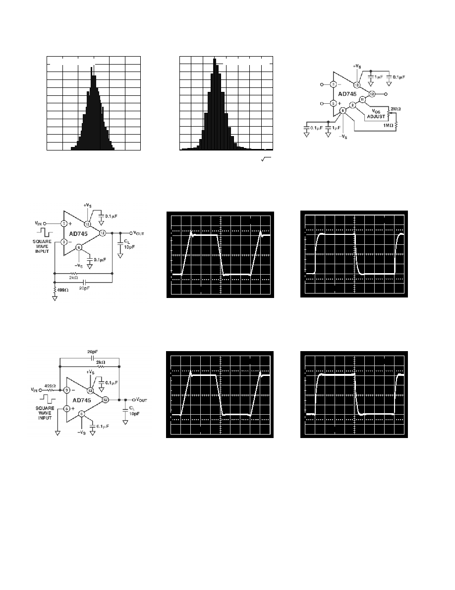
TPC 19. Distribution of Offset
Voltage Drift. T
A
= 25
°C to 125°C
TPC 22a. Gain of 5 Follower,
16-Lead Package Pinout
TPC 23a. Gain of 4 Inverter,
16-Lead Package Pinout
INPUT VOLTAGE NOISE @ 10kHz nV Hz
NUMBER OF UNITS
648
2.6
2.7
3.2
2.8
2.9
3.0
3.1
594
540
486
432
378
324
270
216
162
108
54
0
TOTAL UNITS = 4100
3.3
3.4
TPC 20. Typical Input Noise Voltage
Distribution @ 10 kHz
2µs
5V
100
90
10
0%
TPC 22b. Gain of 5 Follower
Large Signal Pulse Response
2µs
5V
100
90
10
0%
TPC 23b. Gain of 4 Inverter Large
Signal Pulse Response
TPC 21. Offset Null Configuration,
16-Lead Package Pinout
500ns
50mV
100
90
10
0%
TPC 22c. Gain of 5 Follower Small
Signal Pulse Response
500ns
50mV
100
90
10
0%
TPC 23c. Gain of 4 Inverter Small
Signal Pulse Response
REV. D
AD745
7
OP AMP PERFORMANCE JFET VERSUS BIPOLAR
The AD745 offers the low input voltage noise of an industry
standard bipolar opamp without its inherent input current
errors. This is demonstrated in Figure 3, which compares input
voltage noise vs. input source resistance of the OP37 and the
AD745 opamps. From this figure, it is clear that at high source
impedance the low current noise of the AD745 also provides
lower total noise. It is also important to note that with the AD745
this noise reduction extends all the way down to low source
impedances. The lower dc current errors of the AD745 also
reduce errors due to offset and drift at high source impedances
(Figure 4).
The internal compensation of the AD745 is optimized for higher
gains, providing a much higher bandwidth and a faster slew
rate. This makes the AD745 especially useful as a preamplifier,
where low-level signals require an amplifier that provides both
high amplification and wide bandwidth at these higher gains.
SOURCE RESISTANCE
1000
100
INPUT NOISE
V
O
L
T
A
GE
nV/ Hz 100
10
1
1k
10k
100k
1M
10M
R
SOURCE
R
SOURCE
E
O
OP37 AND
RESISTOR
AD745 AND
RESISTOR
AD745 AND RESISTOR
OR
OP37 AND RESISTOR
RESISTOR NOISE ONLY
Figure 3. Total Input Noise Spectral Density @ 1 kHz
vs. Source Resistance
SOURCE RESISTANCE
100
10
0.1
100
10M
1k
INPUT OFFSET
V
O
L
T
A
GE
mV
10k
100k
1M
1.0
OP37G
AD745 KN
Figure 4. Input Offset Voltage vs. Source Resistance
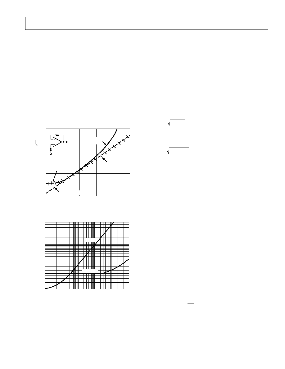
DESIGNING CIRCUITS FOR LOW NOISE
An opamp's input voltage noise performance is typically divided
into two regions: flatband and low frequency noise. The AD745
offers excellent performance with respect to both. The figure of
2.9 nV/ Hz @ 10 kHz is excellent for a JFET input amplifier.
The 0.1 Hz to 10 Hz noise is typically 0.38
µV p-p. The user
should pay careful attention to several design details to optimize
low frequency noise performance. Random air currents can
generate varying thermocouple voltages that appear as low
frequency noise. Therefore, sensitive circuitry should be well
shielded from air flow. Keeping absolute chip temperature low
also reduces low frequency noise in two ways: first, the low
frequency noise is strongly dependent on the ambient tempera-
ture and increases above 25
°C. Second, since the gradient of
temperature from the IC package to ambient is greater, the
noise generated by random air currents, as previously mentioned,
will be larger in magnitude. Chip temperature can be reduced
both by operation at reduced supply voltages and by the use of a
suitable clip-on heat sink, if possible.
Low frequency current noise can be computed from the
magnitude of the dc bias current
~
I
n
= 2qI
B
f
and increases below approximately 100 Hz with a 1/f power
spectral density. For the AD745 the typical value of current
noise is 6.9 fA/
Hz at 1 kHz. Using the formula:
I
~
n
= 4kT/Rf
to compute the Johnson noise of a resistor, expressed as a
current, one can see that the current noise of the AD745 is
equivalent to that of a 3.45
× 10
8
source resistance.
At high frequencies, the current noise of a FET increases pro-
portionately to frequency. This noise is due to the "real" part of
the gate input impedance, which decreases with frequency. This
noise component usually is not important, since the voltage
noise of the amplifier impressed upon its input capacitance is an
apparent current noise of approximately the same magnitude.
In any FET input amplifier, the current noise of the internal
bias circuitry can be coupled externally via the gate-to-source
capacitances and appears as input current noise. This noise is
totally correlated at the inputs, so source impedance matching
will tend to cancel out its effect. Both input resistance and input
capacitance should be balanced whenever dealing with source
capacitances of less than 300 pF in value.
LOW NOISE CHARGE AMPLIFIERS
As stated, the AD745 provides both low voltage and low current
noise. This combination makes this device particularly suitable
in applications requiring very high charge sensitivity, such as
capacitive accelerometers and hydrophones. When dealing with
a high source capacitance, it is useful to consider the total input
charge uncertainty as a measure of system noise.
Charge (Q) is related to voltage and current by the simply stated
fundamental relationships:
Q
= CV and I =
dQ
dt
As shown, voltage, current and charge noise can all be directly
related. The change in open circuit voltage (
V) on a capacitor
will equal the combination of the change in charge (
Q/C) and
the change in capacitance with a built-in charge (Q/
C).
REV. D
AD745
8
Figures 5 and 6 show two ways to buffer and amplify the output
of a charge output transducer. Both require the use of an ampli-
fier that has a very high input impedance, such as the AD745.
Figure 5 shows a model of a charge amplifier circuit. Here,
amplification depends on the principle of conservation of charge
at the input of amplifier A1, which requires that the charge on
capacitor C
S
be transferred to capacitor C
F
, thus yielding an
output voltage of
Q/C
F
. The amplifiers input voltage noise will
appear at the output amplified by the noise gain (1 + (C
S
/C
F
))
of the circuit.
A1
C
B
*
R
B
*
C
S
R2
R1
R
S
C
F
R1
R2
C
S
C
F
=
Figure 5. A Charge Amplifier Circuit
R
B
C
S
A2
C
B
*
R1
R2
R
B
*
*OPTIONAL, SEE TEXT.
Figure 6. Model for A High Z Follower with Gain
The second circuit, Figure 6, is simply a high impedance fol-
lower with gain. Here the noise gain (1 + (R1/R2)) is the same
as the gain from the transducer to the output. Resistor R
B
, in
both circuits, is required as a dc bias current return.
There are three important sources of noise in these circuits.
Amplifiers A1 and A2 contribute both voltage and current noise,
while resistor R
B
contributes a current noise of:
~
N
k
T
R
f
B
= 4
where:
k = Boltzman's Constant = 1.381
× 10
23
Joules/Kelvin
T = Absolute Temperature, Kelvin (0
°C = 273.2 Kelvin)
f = Bandwidth in Hz (Assuming an Ideal "Brick Wall"
Filter)
This must be root-sum-squared with the amplifier's own current
noise.
Figure 5 shows that these two circuits have an identical frequency
response and the same noise performance (provided that
C
S
/C
F
= R1/ R2). One feature of the first circuit is that a "T"
network is used to increase the effective resistance of R
B
and
improve the low frequency cutoff point by the same factor.
FREQUENCY Hz
100
0.01
DECIBELS REFERENCED
T
O
1V/ Hz
110
120
130
140
150
160
170
180
190
200
210
220
0.1
1
10
100
1k
10k
100k
TOTAL
OUTPUT
NOISE
NOISE DUE TO
R
B
ALONE
NOISE DUE TO
I
B
ALONE
Figure 7. Noise at the Outputs of the Circuits of Figures 5
and 6. Gain = 10, C
S
= 3000 pF, R
B
= 22 M
However, this does not change the noise contribution of R
B
which, in this example, dominates at low frequencies. The graph
of Figure 8 shows how to select an R
B
large enough to minimize
this resistor's contribution to overall circuit noise. When the
equivalent current noise of R
B
(( 4 kT)/R) equals the noise of
I
B
2
qI
B
(
)
, there is diminishing return in making R
B
larger.
INPUT BIAS CURRENT
5.2 10
10
1pA
10nA
10pA
RESIST
ANCE IN
100pA
1nA
5.2 10
9
5.2 10
8
5.2 10
7
5.2 10
6
Figure 8. Graph of Resistance vs. Input Bias Current
Where the Equivalent Noise
4 kT/R, Equals the Noise
of the Bias Current
I
B
2
qI
B
(
)
To maximize dc performance over temperature, the source
resistances should be balanced on each input of the amplifier.
This is represented by the optional resistor R
B
in Figures 5 and 6.
As previously mentioned, for best noise performance care should
be taken to also balance the source capacitance designated by
C
B
The value for C
B
in Figure 5 would be equal to C
S
in
Figure 6. At values of C
B
over 300 pF, there is a diminishing
impact on noise; capacitor C
B
can then be simply a large mylar
bypass capacitor of 0.01
µF or greater.
REV. D
AD745
9
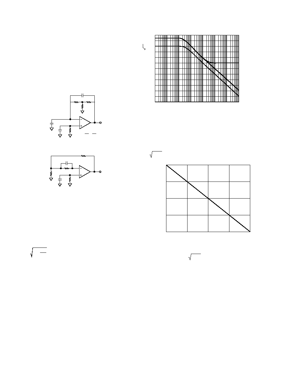
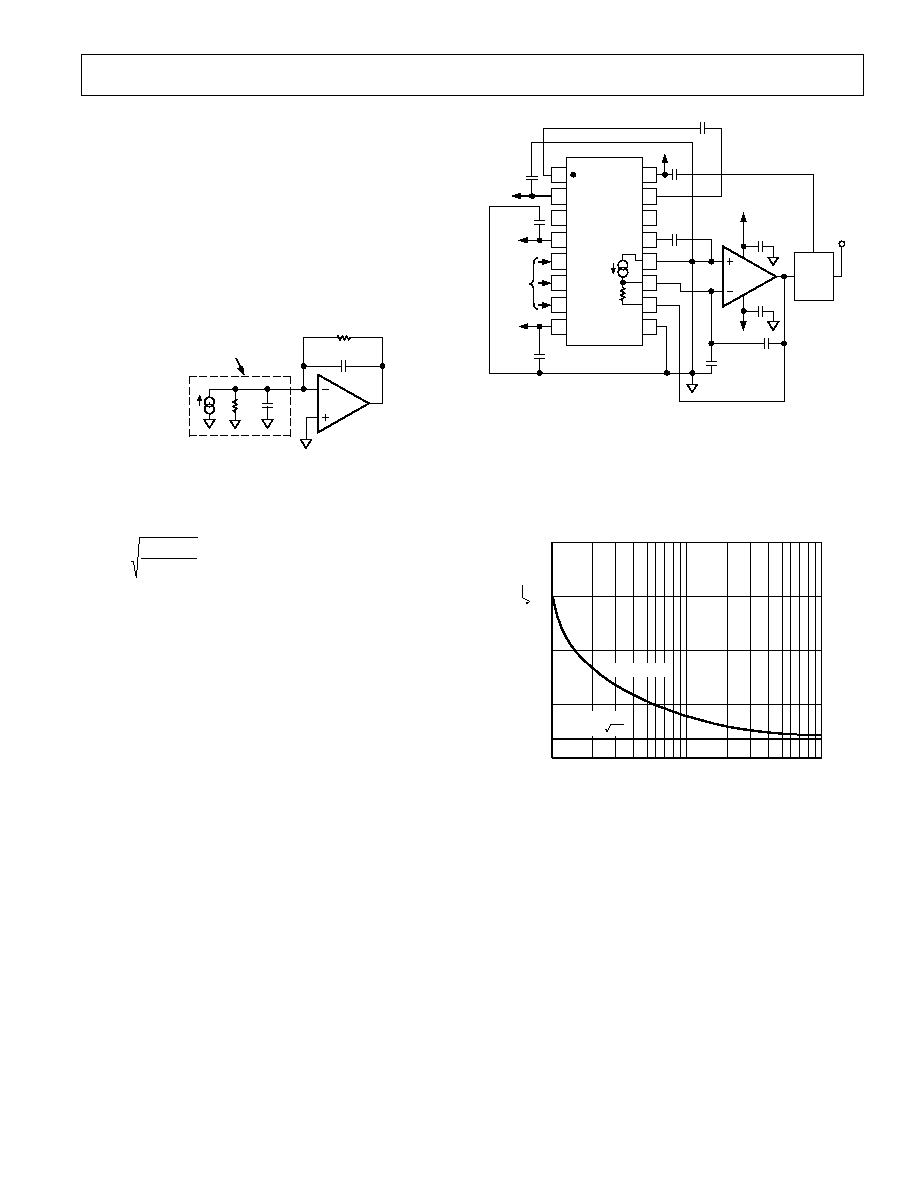
HOW CHIP PACKAGE TYPE AND POWER DISSIPATION
AFFECT INPUT BIAS CURRENT
As with all JFET input amplifiers, the input bias current of the
AD745 is a direct function of device junction temperature, I
B
approximately doubling every 10
°C. Figure 9 shows the rela-
tionship between bias current and junction temperature for the
AD745. This graph shows that lowering the junction tempera-
ture will dramatically improve I
B
.
JUNCTION TEMPERATURE C
10
6
60
INPUT BIAS CURRENT
Amps
10
7
10
8
10
9
10
10
10
11
10
12
40
20
0
20
40
60
80
100
120
140
V
S
= 15V
T
A
= 25 C
Figure 9. Input Bias Current vs. Junction Temperature
The dc thermal properties of an IC can be closely approximated
by using the simple model of Figure 10 where current represents
power dissipation, voltage represents temperature, and resistors
represent thermal resistance (
in °C/watt).
T
A
JA
JC
CA
T
J
P
IN
WHERE:
P
IN
= DEVICE DISSIPATION
T
A
= AMBIENT TEMPERATURE
T
J
= JUNCTION TEMPERATURE
JC
= THERMAL RESISTANCE JUNCTION TO CASE
CA
= THERMAL RESISTANCE CASE TO AMBIENT
Figure 10. Device Thermal Model
From this model T
J
= T
A
+
JA
P
IN
. Therefore, I
B
can be deter-
mined in a particular application by using Figure 9 together with
the published data for
JA
and power dissipation. The user can
modify
JA
by use of an appropriate clip-on heat sink such as the
Aavid #5801. Figure 11 shows bias current versus supply voltage
with
JA
as the third variable. This graph can be used to predict
bias current after
JA
has been computed. Again bias current will
double for every 10
°C.
SUPPLY VOLTAGE Volts
300
5
15
10
INPUT BIAS CURRENT
Amps
200
100
0
T
A
= 25 C
JA
= 165 C/W
JA
= 115 C/W
JA
= 0 C/W
Figure 11. Input Bias Current vs. Supply Voltage for
Various Values of
JA
A
(J TO DIE
MOUNT)
B
(DIE MOUNT
TO CASE)
A
+
B
=
JC
T
J
T
A
CASE
Figure 12. Breakdown of Various Package Thermal
Resistance
REDUCED POWER SUPPLY OPERATION FOR
LOWER I
B
Reduced power supply operation lowers I
B
in two ways: first, by
lowering both the total power dissipation and, second, by reduc-
ing the basic gate-to-junction leakage (Figure 11). Figure 13
shows a 40 dB gain piezoelectric transducer amplifier, which
operates without an ac coupling capacitor, over the 40
°C to
+85
°C temperature range. If the optional coupling capacitor,
C1, is used, this circuit will operate over the entire 55
°C to
+125
°C temperature range.
+5V
5V
CT**
C1*
100
10k
10
8
**
C
T
10
8
TRANSDUCER
*OPTIONAL DC BLOCKING CAPACITOR
**OPTIONAL, SEE TEXT
AD745
Figure 13. A Piezoelectric Transducer
REV. D
AD745
10
TWO HIGH PERFORMANCE ACCELEROMETER
AMPLIFIERS
Two of the most popular charge-out transducers are hydrophones
and accelerometers. Precision accelerometers are typically cali-
brated for a charge output (pC/g).
*
Figures 14 and 15 show two
ways in which to configure the AD745 as a low noise charge
amplifier for use with a wide variety of piezoelectric accelerom-
eters. The input sensitivity of these circuits will be determined
by the value of capacitor C1 and is equal to:
V
OUT
=
Q
OUT
C1
The ratio of capacitor C1 to the internal capacitance (C
T
) of the
transducer determines the noise gain of this circuit (1 + C
T
/C1).
The amplifiers voltage noise will appear at its output amplified
by this amount. The low frequency bandwidth of these circuits
will be dependent on the value of resistor R1. If a "T" network
is used, the effective value is: R1 (1 + R2/R3).
*
pC = Picocoulombs
g = Earth's Gravitational Constant
R3
1k
R2
9k
R1
110M
(5 22M )
C1
1250pF
B AND K
4370 OR
EQUIVALENT
OUTPUT
0.8mV/pC
AD745
Figure 14. A Basic Accelerometer Circuit
R3
1k
R2
9k
R1
110M
(5 22M )
C1
1250pF
AD745
B AND K
4370 OR
EQUIVALENT
OUTPUT
0.8mV/pC
AD711
C2
2.2 F
R4
18M
R5
18M
C3
2.2 F
Figure 15. An Accelerometer Circuit Employing a DC
Servo Amplifier
A dc servo loop (Figure 15) can be used to assure a dc output
<10 mV, without the need for a large compensating resistor
when dealing with bias currents as large as 100 nA. For optimal
low frequency performance, the time constant of the servo loop
(R4C2 = R5C3) should be:
Time Constant
10 R1 1+
R2
R3
C1
A LOW NOISE HYDROPHONE AMPLIFIER
Hydrophones are usually calibrated in the voltage-out mode.
The circuit of Figures 16 can be used to amplify the output of a
typical hydrophone. If the optional ac coupling capacitor C
C
is
used, the circuit will have a low frequency cutoff determined by
an RC time constant equal to:
Time Constant
×
×
10
1
1
2
100
R
C
C
where the dc gain is 1 and the gain above the low frequency
cutoff (1/(2
C
C
(100
))) is equal to (1 + R2/R3). The circuit
of Figure 17 uses a dc servo loop to keep the dc output at 0 V
and to maintain full dynamic range for I
B
's up to 100 nA. The
time constant of R7 and C1 should be larger than that of R1
and C
T
for a smooth low frequency response.
C1*
C
C
R3
100
R2
1900
R4*
C
T
R1
10
8
B AND K TYPE 8100 HYDROPHONE
AD745
OUTPUT
INPUT SENSITIVITY = 179dB RE. 1V/mPa**
*OPTIONAL DC BLOCKING CAPACITOR
**OPTIONAL, SEE TEXT
Figure 16. A Low Noise Hydrophone Amplifier
The transducer shown has a source capacitance of 7500 pF. For
smaller transducer capacitances (
300 pF), lowest noise can be
achieved by adding a parallel RC network (R4 = R1, C1 = C
T
)
in series with the inverting input of the AD745.
C1*
R3
100
R2
1900
C
T
R4*
10
8
AD745
OUTPUT
AD711K
R1
10
8
16M
C2
0.27 F
R5
100k
R4
16M
R6
1M
DC OUTPUT 1mV FOR IB (AD745) 100nA
*OPTIONAL, SEE TEXT
Figure 17. A Hydrophone Amplifier Incorporating a DC
Servo Loop
REV. D
AD745
11
DESIGN CONSIDERATIONS FOR I-TO-V CONVERTERS
There are some simple rules of thumb when designing an I-V
converter where there is significant source capacitance (as with
a photodiode) and bandwidth needs to be optimized. Consider
the circuit of Figure 18. The high frequency noise gain
(1 + C
S
/C
L
) is usually greater than five, so the AD745, with its
higher slew rate and bandwidth is ideally suited to this applica-
tion.
Here both the low current and low voltage noise of the AD745 can
be taken advantage of, since it is desirable in some instances to
have a large R
F
(which increases sensitivity to input current noise)
and, at the same time, operate the amplifier at high noise gain.
AD745
I
S
R
B
C
S
C
L
R
F
INPUT SOURCE: PHOTO DIODE,
ACCELEROMETER, ECT.
Figure 18. A Model for an l-to-V Converter
In this circuit, the R
F
C
S
time constant limits the practical band-
width over which flat response can be obtained, in fact:
f
B
f
C
2
R
F
C
S
where:
f
B
= signal bandwidth
f
C
= gain bandwidth product of the amplifier
With C
L
1/(2 R
F
C
S
) the net response can be adjusted to a
provide a two pole system with optimal flatness that has a corner
frequency of f
B
. Capacitor C
L
adjusts the damping of the circuit's
response. Note that bandwidth and sensitivity are directly traded
off against each other via the selection of R
F
. For example, a
photodiode with C
S
= 300 pF and R
F
= 100 k
will have a maxi-
mum bandwidth of 360 kHz when capacitor C
L
4.5 pF.
Conversely, if only a 100 kHz bandwidth were required, then
the maximum value of R
F
would be 360 k
and that of capaci-
tor C
L
still
4.5 pF.
In either case, the AD745 provides impedance transformation,
the effective transresistance, i.e., the I/V conversion gain, may
be augmented with further gain. A wideband low noise amplifier
such as the AD829 is recommended in this application.
This principle can also be used to apply the AD745 in a high
performance audio application. Figure 19 shows that an I-V
converter of a high performance DAC, here the AD1862, can
be designed to take advantage of the low voltage noise of the
AD745 (2.9 nV/ Hz) as well as the high slew rate and band-
width provided by decompensation. This circuit, with component
values shown, has a 12 dB/octave rolloff at 728 kHz, with a
passband ripple of less than 0.001 dB and a phase deviation of
less than 2 degrees @ 20 kHz.
0.1 F
AD745
0.1 F
+12V
12V
100pF
2000pF
10 F
+
DIGITAL
COMMON
0.01 F
12V
AD1862
20-BIT D/A
CONVERTER
3k
TOP VIEW
3 POLE
LOW
PASS
FILTER
OUTPUT
0.01 F
ANALOG
COMMON
+12V
DIGITAL
INPUTS
+12V
0.01 F
12V
0.01 F
1 F
+
16
15
14
13
12
11
10
9
1
2
3
4
5
6
7
8
Figure 19. A High Performance Audio DAC Circuit
An important feature of this circuit is that high frequency en-
ergy, such as clock feedthrough, is shunted to common via a
high quality capacitor and not the output stage of the amplifier,
greatly reducing the error signal at the input of the amplifier and
subsequent opportunities for intermodulation distortions.
INPUT CAPACITANCE pF
40
30
0
10
1k
100
R
T
I NOISE
V
O
L
T
A
GE
nV/ Hz
20
10
BALANCED
2.9nV/ Hz
UNBALANCED
Figure 20. RTI Noise Voltage vs. Input Capacitance
BALANCING SOURCE IMPEDANCES
As mentioned previously, it is good practice to balance the
source impedances (both resistive and reactive) as seen by the
inputs of the AD745. Balancing the resistive components will
optimize dc performance over temperature because balancing
will mitigate the effects of any bias current errors. Balancing
input capacitance will minimize ac response errors due to the
amplifier's input capacitance and, as shown in Figure 20, noise
performance will be optimized. Figure 21 shows the required
external components for noninverting (A) and inverting (B)
configurations.
REV. D
12
C0083103/02(D)
PRINTED IN U.S.A.
AD745
OUTLINE DIMENSIONS
Dimensions shown in inches and (mm).
16-Lead SOIC (R) Package
SEATING
PLANE
0.0118 (0.30)
0.0040 (0.10)
0.0192 (0.49)
0.0138 (0.35)
0.1043 (2.65)
0.0926 (2.35)
0.050 (1.27)
BSC
16
9
8
1
0.4193 (10.65)
0.3937 (10.00)
0.2992 (7.60)
0.2914 (7.40)
PIN 1
0.4133 (10.50)
0.3977 (10.00)
0.0125 (0.32)
0.0091 (0.23)
8
0
0.0291 (0.74)
0.0098 (0.25)
45
0.0500 (1.27)
0.0157 (0.40)
Figure 40. Optional External Components for Balancing Source Impedances
AD745
R
S
C
S
C
F
R
1
OUTPUT
C
B
R
B
INVERTING
CONNECTION
C
B
= C
F
|| C
S
R
B
= R
1
|| R
S
AD745
R
2
C
B
R
1
OUTPUT
C
S
R
S
NONINVERTING
CONNECTION
R
B
C
B
= C
S
R
B
= R
S
FOR
R
S
>> R
1
OR R
2
Revision History
Location
Page
Data Sheet changed from REV. C to REV. D.
Deleted 8-Lead Plastic Mini-DIP (N) and 8-Lead Cerdip (Q) Packages from CONNECTION DIAGRAM . . . . . . . . . . . . . . . . . . 1
Edits to PRODUCT DESCRIPTION . . . . . . . . . . . . . . . . . . . . . . . . . . . . . . . . . . . . . . . . . . . . . . . . . . . . . . . . . . . . . . . . . . . . . . . . 1
Edits to ELECTRICAL CHARACTERISTICS . . . . . . . . . . . . . . . . . . . . . . . . . . . . . . . . . . . . . . . . . . . . . . . . . . . . . . . . . . . . . . . . 2
Edits to ABSOLUTE MAXIMUM RATINGS . . . . . . . . . . . . . . . . . . . . . . . . . . . . . . . . . . . . . . . . . . . . . . . . . . . . . . . . . . . . . . . . . 3
Edits to ORDERING GUIDE . . . . . . . . . . . . . . . . . . . . . . . . . . . . . . . . . . . . . . . . . . . . . . . . . . . . . . . . . . . . . . . . . . . . . . . . . . . . . . 3
Deleted to METALIZATION PHOTOGRAPH . . . . . . . . . . . . . . . . . . . . . . . . . . . . . . . . . . . . . . . . . . . . . . . . . . . . . . . . . . . . . . . . 3
Deleted text from HOW CHIP PACKAGE TYPE AND POWER DISSIPATION AFFECT INPUT BIAS CURRENT . . . . . . . . 9
Deleted 8-Lead Plastic Mini-DIP (N) and 8-Lead Cerdip (Q) Packages from OUTLINE DIMENSIONS . . . . . . . . . . . . . . . . . . 12