 | ÐлекÑÑоннÑй компоненÑ: AD760 | СкаÑаÑÑ:  PDF PDF  ZIP ZIP |
Äîêóìåíòàöèÿ è îïèñàíèÿ www.docs.chipfind.ru
FUNCTIONAL BLOCK DIAGRAM
REV. A
Information furnished by Analog Devices is believed to be accurate and
reliable. However, no responsibility is assumed by Analog Devices for its
use, nor for any infringements of patents or other rights of third parties
which may result from its use. No license is granted by implication or
otherwise under any patent or patent rights of Analog Devices.
a
16/18-Bit Self-Calibrating
Serial/Byte DACPORT
AD760
© Analog Devices, Inc., 1995
One Technology Way, P.O. Box 9106, Norwood. MA 02062-9106, U.S.A.
Tel: 617/329-4700
Fax: 617/326-8703
FEATURES
±0.2 LSB (±0.00031%) Typ Peak DNL and INL
±0.5 LSB (±0.00076%) Typ Unipolar Offset, Bipolar Zero
17-Bit Monotonicity Guaranteed
18-Bit Resolution (in Serial Mode)
Complete 16/18-Bit D/A Function
On-Chip Output Amplifier
On-Chip Buried Zener Voltage Reference
Microprocessor Compatible
Serial or Byte Input
Double Buffered Latches
Asynchronous Clear Function
Serial Output Pin Facilitates Daisy Chaining
Pin Strappable Unipolar or Bipolar Output
Low THD+N: 0.005%
MUX Output Control on Power-Up and Supply Glitches
+10V
REF
10k
S
OUT
SPAN/
BIP
OFF
V
OUT
9.95k
LDAC
REF IN
REF OUT
HBE
SER
CLR
10k
AD760
UNI
/
BIP CLR
OR
LBE
MUX
OUT
MUX
I N
AGND
S
IN
OR
DB0
DB2
DB7
CS
MSB/
LSB
OR
DB1
12
18/16
SERIAL
OR
24
23
15
27
28
22
25
17
18
20
21
19
MAIN DAC
CONTROL
LOGIC
16
26
RAM
CALIBRATION SEQUENCER
CALOK
V
EE
+V
CC
+V
LL
DGND
CAL
1
2
3
5
6
4
14
16/18-BIT
INPUT REGISTER
13
7
CALIBRATION DAC
16/18-BIT DAC LATCH
Typical Integral Nonlinearity
DACPORT is a registered trademark of Analog Devices, Inc.
0.75
0.25
0
0.25
0.75
0
16384
32768
49152
65535
INPUT CODE Decimal
RELATIVE ACCURACY LSB
V
OUT
= 10V TO +10V
R
L
= 2k
C
L
= 1000pF
MUX output in a predetermined state by means of a digital and
analog power supply detection circuit. This is particularly use-
ful for robotic and industrial control applications.
The AD760 is available in a 28-pin, 600 mil cerdip package.
The AQ version is specified from 40°C to +85°C.
PRODUCT DESCRIPTION
The AD760 is a complete 16/18-bit self-calibrating monolithic
DAC (DACPORT®) with onboard voltage reference, double
buffered latches and output amplifier. It is manufactured on
Analog Devices' BiMOS II process. This process allows the fab-
rication of low power CMOS logic functions on the same chip
as high precision bipolar linear circuitry.
Self-calibration is initiated by simply pulsing the CAL pin low.
The CALOK pin indicates when calibration has been success-
fully completed. The output multiplexer (MUX
OUT
) can be used
to send the output to the bottom of the output range during
calibration.
Data can be loaded into the AD760 as straight binary, serial
data or as two 8-bit bytes. In serial mode, 16-bit or 18-bit data
can be used and the serial mode input format is pin selectable,
to be MSB or LSB first. This is made possible by three digital
input pins which have dual functions (Pins 12, 13, and 14). In
byte mode the user can similarly define whether the high byte or
low byte is loaded first. The serial output (S
OUT
) pin allows the
user to daisy chain several AD760s by shifting the data through
the input latch into the next DAC thus minimizing the number
of control lines required in a multiple DAC application. The
double buffered latch structure eliminates data skew errors and
provides for simultaneous updating of DACs in a multi-DAC
system.
The asynchronous CLR function can be configured to clear the
output to minus full-scale or midscale depending on the state of
Pin 17 when CLR is strobed. The AD760 also powers up with the

AD760AQ
Model
Min
Typ
Max
Units
RESOLUTION
1
16/18
Bits
TRANSFER FUNCTION CHARACTERISTICS
2
With Calibration @ T
CAL
3
;
40°C T
CAL
+85°C
Integral Nonlinearity
±0.2
±0.75
16-Bit LSB
Differential Nonlinearity
±0.2
±0.5
16-Bit LSB
Monotonicity
17
18
Bits
Unipolar Offset
±0.5
±1
16-Bit LSB
Bipolar Zero Error
±0.5
±1
16-Bit LSB
Without Calibration
Integral Nonlinearity
±2
16-Bit LSB
T
MIN
to T
MAX
±4
16-Bit LSB
Integral Nonlinearity Drift
0.015
16-Bit LSB/°C
Differential Nonlinearity
±2
16-Bit LSB
T
MIN
to T
MAX
±4
16-Bit LSB
Differential Nonlinearity Drift
0.015
16-Bit LSB/°C
Monotonicity Over Temperature
14
Bits
Unipolar Offset
±2.5
mV
Unipolar Offset Drift (T
MIN
to T
MAX
)
3
ppm/°C
Bipolar Zero Error
±10
mV
Bipolar Zero Error Drift (T
MIN
to T
MAX
)
5
ppm/°C
Gain Error
4, 5
±0.10
% of FSR
Gain Drift
5
(T
MIN
to T
MAX
)
25
ppm/°C
DAC Gain Error
6
±0.05
% of FSR
DAC Gain Drift
6
(T
MIN
to T
MAX
)
10
ppm/°C
INPUT RESISTANCE
REFIN
7
10
13
k
SPAN/BIP OFF
7
10
13
k
REFERENCE OUTPUT
Voltage
9.99
10.00
10.01
V
Drift
25
ppm/°C
External Current
7
2
4
mA
Capacitive Load
1000
pF
Short Circuit Current
25
mA
Long-Term Stability
50
ppm/1000 Hrs
OUTPUT CHARACTERISTICS
2
Output Voltage Range
Unipolar Configuration
0
+10
V
Bipolar Configuration
10
+10
V
Output Current
5
mA
Capacitive Load
1000
pF
Short Circuit Current
25
mA
MUX
OUT
Resistance
0.9
7
k
DIGITAL INPUTS (T
MIN
to T
MAX
)
V
IH
(Logic "1")
2.0
V
LL
V
V
IL
(Logic "0")
0
0.8
V
I
IH
(V
IH
= V
LL
)
±10
µA
I
IL
(V
IL
= 0 V)
±10
µA
DIGITAL OUTPUT (T
MIN
to T
MAX
)
V
OH
(I
OH
= 0.6 mA)
2.4
V
V
OL
(I
OL
= 1.6 mA)
0.4
V
POWER SUPPLIES
Voltage
V
CC
8
+14.25
+15.75
V
V
EE
8
15.75
14.25
V
V
LL
+4.75
+5.25
V
Current (No Load)
I
CC
+18
+21
mA
I
EE
21
18
mA
I
LL
@ V
IH
, V
IL
= 5.0 V, 0 V
2
3
mA
@ V
IH
, V
IL
= 2.4 V, 0.4 V
3
7.5
mA
Power Supply Sensitivity with V
OUT
= 10 V
1
ppm/%
Power Dissipation (Static, No Load)
600
725
mW
TEMPERATURE RANGE
Specified Performance (A)
40
+85
°C
AD760SPECIFICATIONS
REV. A
2
(@ T
A
= +25°C, V
CC
= +15 V, V
EE
= 15 V, V
LL
= + 5 V, unless otherwise noted)
AD760
REV. A
3
NOTES
1
For 18-bit resolution, 1 LSB = 0.00038% of FSR. For 16-bit resolution, 1 LSB = 0.0015% of FSR. For 14-bit resolution, 1 LSB = 0.006% of FSR. FSR stands for
full-scale range and is 10 V in unipolar mode and 20 V in bipolar mode.
2
Characteristics are guaranteed at V
OUT
Pin (23).
3
T
CAL
is the calibration temperature.
4
Gain Error is measured with a fixed 50 resistor as shown in Figure 5a and Figure 6a.
5
Gain Error and gain drift are measured with the internal reference. The internal reference is the main contributor to the gain drift. If lower drift is required, the
AD760 can be used with a precision external reference such as the AD587, AD586 or AD688.
6
DAC Gain Error is measured without the on-chip voltage reference. It represents the performance that can be obtained with an external precision reference.
7
External current is defined as the current available in addition to that supplied to REF IN and SPAN/BIPOLAR OFFSET on the AD760.
8
Operation on ±12 V supplies is possible using an external reference such as the AD586 and reducing the output range. Refer to the Internal/External Reference
section.
Specifications subject to change without notice.
AC PERFORMANCE CHARACTERISTICS
Parameter
Limit
Units
Test Conditions/Comments
Output Settling Time
13
µs max
20 V Step, T
A
= +25°C
(Time to +0.0008% FS, with
8
µs typ
20 V Step, T
A
= +25°C
2 k , 1000 pF Load)
10
µs typ
20 V Step
6
µs typ
10 V Step, T
A
= +25°C
8
µs typ
10 V Step
2.5
µs typ
1 LSB Step
MUX
OUT
Recovery Time
Recovery time is referenced to the rising edge of CALOK,
(Time to +0.0008% FS, with
when MUX
OUT
switches from MUX
IN
to V
OUT
.
100 pF Load)
MUX
IN
= V
OUT
prior to calibration.
2
µs typ
MUX
IN
, V
OUT
= 10 V to +10 V
Total Harmonic Distortion + Noise
A, S Grade
0.005
% max
0 dB, 1001 Hz. Sample Rate = 100 kHz. T
A
= +25°C
A, S Grade
0.03
% max
20 dB, 1001 Hz. Sample Rate = 100 kHz. T
A
= +25°C
A, S Grade
3.0
% max
60 dB, 1001 Hz. Sample Rate = 100 kHz. T
A
= +25°C
Signal-to-Noise Ratio
94
dB min
T
A
= +25°C, byte load
Digital-to-Analog Glitch Impulse
15
nV-s typ
DAC alternately loaded with 8000
H
and 7FFF
H
MUX
OUT
Glitch Impulse
30
nV-s typ
100 pF Load. MUX
IN
= V
OUT
= negative full scale
Digital Feedthrough
2
nV-s typ
DAC alternately loaded with 0000
H
and FFFF
H
. CS high
Output Noise Voltage Density (1 kHz1 MHz)
120
nV/ Hz typ
Measured at V
OUT
, 20 V span, excludes internal reference
Reference Noise (1 kHz1 MHz)
125
nV/ Hz typ
Measured at REF OUT
Specifications are subject to change without notice.
With the exception of Total Harmonic Distortion + Noise and Signal-to-Noise
Ratio, these characteristics are included for design guidance only and are not subject to test. THD+N and SNR are 100% tested. (T
MIN
< T
A
< T
MAX
, V
CC
= +15 V, V
EE
= 15 V, V
LL
= +5 V, tested at V
OUT
except where noted.)
4
AD760
REV. A
(V
CC
= +15 V, V
EE
= 15 V, V
LL
= +5 V, V
IH
= 2.4 V, V
IL
= 0.4 V)
TIMING CHARACTERISTICS
Limit
Parameter
+25°C
T
MIN
to T
MAX
Units
(Figure 1a)
t
CS
50
60
ns min
t
DS
50
60
ns min
t
DH
0
10
ns min
t
BES
50
60
ns min
t
BEH
0
10
ns min
t
LH
200
350
ns min
t
LW
50
50
ns min
(Figure 1b)
t
CLK
80
100
ns min
t
LO
40
50
ns min
t
HI
40
50
ns min
t
DS
50
60
ns min
t
DH
0
10
ns min
t
LH
200
350
ns min
t
LW
50
50
ns min
t
PROP
70
100
ns max
Limit
Parameter
+25°C
T
MIN
to T
MAX
Units
(Figure 1c)
t
CLR
100
120
ns min
t
SET
100
120
ns min
t
HOLD
0
0
ns min
(Figure 1d)
t
CAL
50
50
ns min
t
BUSY
200
200
ms max
t
CD
170
220
ns max
t
CS
150
190
ns max
t
CV
150
190
ns max
Specifications subject to change without notice.
DB07
t
DS
t
DH
t
BES
t
CS
t
BEH
t
LH
t
LW
HBE
OR
LBE
CS
LDAC
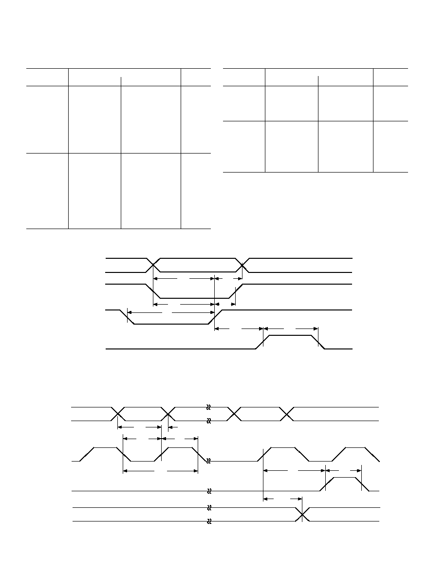
Figure 1a. AD760 Byte Load Timing
SIN
LDAC
VALID 1
VALID 16/18
t
DS
t
LO
t
H I
S
OUT
VALID 1
CS
t
D H
t
LH
t
LW
t
PROP
t
CLK
Figure 1b. AD760 Serial Load Timing
AD760
REV. A
5
ORDERING GUIDE
Temperature
Package
Package
Model
Range
Description
Option
AD760AQ
40°C to +85°C
Cerdip
Q-28
WARNING!
ESD SENSITIVE DEVICE
CAUTION
ESD (electrostatic discharge) sensitive device. Electrostatic charges as high as 4000 V readily
accumulate on the human body and test equipment and can discharge without detection.
Although the AD760 features proprietary ESD protection circuitry, permanent damage may
occur on devices subjected to high energy electrostatic discharges. Therefore, proper ESD
precautions are recommended to avoid performance degradation or loss of functionality.
ABSOLUTE MAXIMUM RATINGS*
V
CC
to AGND . . . . . . . . . . . . . . . . . . . . . . . 0.3 V to +17.0 V
V
EE
to AGND . . . . . . . . . . . . . . . . . . . . . . . +0.3 V to 17.0 V
V
LL
to DGND . . . . . . . . . . . . . . . . . . . . . . . . . . 0.3 V to +7 V
AGND to DGND . . . . . . . . . . . . . . . . . . . . . . . . . . . . . . ±1 V
Digital Inputs (Pins 2, 714, and 1621)
to DGND . . . . . . . . . . . . . . . . . . . . . . . . . . 1.0 V to +7.0 V
REF IN to AGND . . . . . . . . . . . . . . . . . . . . . . . . . . . . ±10.5 V
Span/Bipolar Offset to AGND . . . . . . . . . . . . . . . . . . . ±10.5 V
REF OUT, V
OUT
, MUX
OUT
, MUX
IN
. . . . . Indefinite Short to
AGND, DGND, V
CC
, V
EE
, and V
LL
JA
, Thermal Impedance . . . . . . . . . . . . . . . . . . . . . . . 50°C/W
Junction Temperature . . . . . . . . . . . . . . . . . . . . . . . . . . 175°C
Storage Temperature . . . . . . . . . . . . . . . . . . 65°C to +150°C
Lead Temperature (Soldering, 10 sec) . . . . . . . . . . . . . +300°C
*
Stresses above those listed under "Absolute Maximum Ratings" may cause
permanent damage to the device. This is a stress rating only and functional
operation of the device at these or any other conditions above those indicated in the
operational section of this specification is not implied. Exposure to absolute
maximum rating conditions for extended periods may affect device reliability.
CALOK
CAL
MUX
IN
DGND
DB7, 15
SPAN/BIP OFF
V
OUT
AGND
V
EE
REF OUT
REF IN
DB6, 14
LDAC
DB5, 13
CLR
DB4, 12
SER
DB3, 11
HBE
DB2, 10, 18/16 SERIAL
LBE, UNI/BIP CLR
DB1, 9, MSB/LSB
CS
DB0, 8, S
IN
S
OUT
13
18
1
2
28
27
5
6
7
24
23
22
3
4
26
25
8
21
9
20
10
19
11
11
12
17
16
14
15
TOP VIEW
(Not to Scale)
AD760
+V
CC
+V
LL
MUX
OUT
PIN CONFIGURATION
DIP
t
CLR
t
HOLD
"1"= BIP, "0"= UNI
t
SET
CLR
UNI
/BIP
CLR
Figure 1c. Asynchronous Clear to Bipolar or Unipolar Zero
t
BUSY
CAL
CALOK
HBE
t
CAL
t
CD
t
CS
t
CV
Figure 1d. Calibration Timing
6
AD760
REV. A
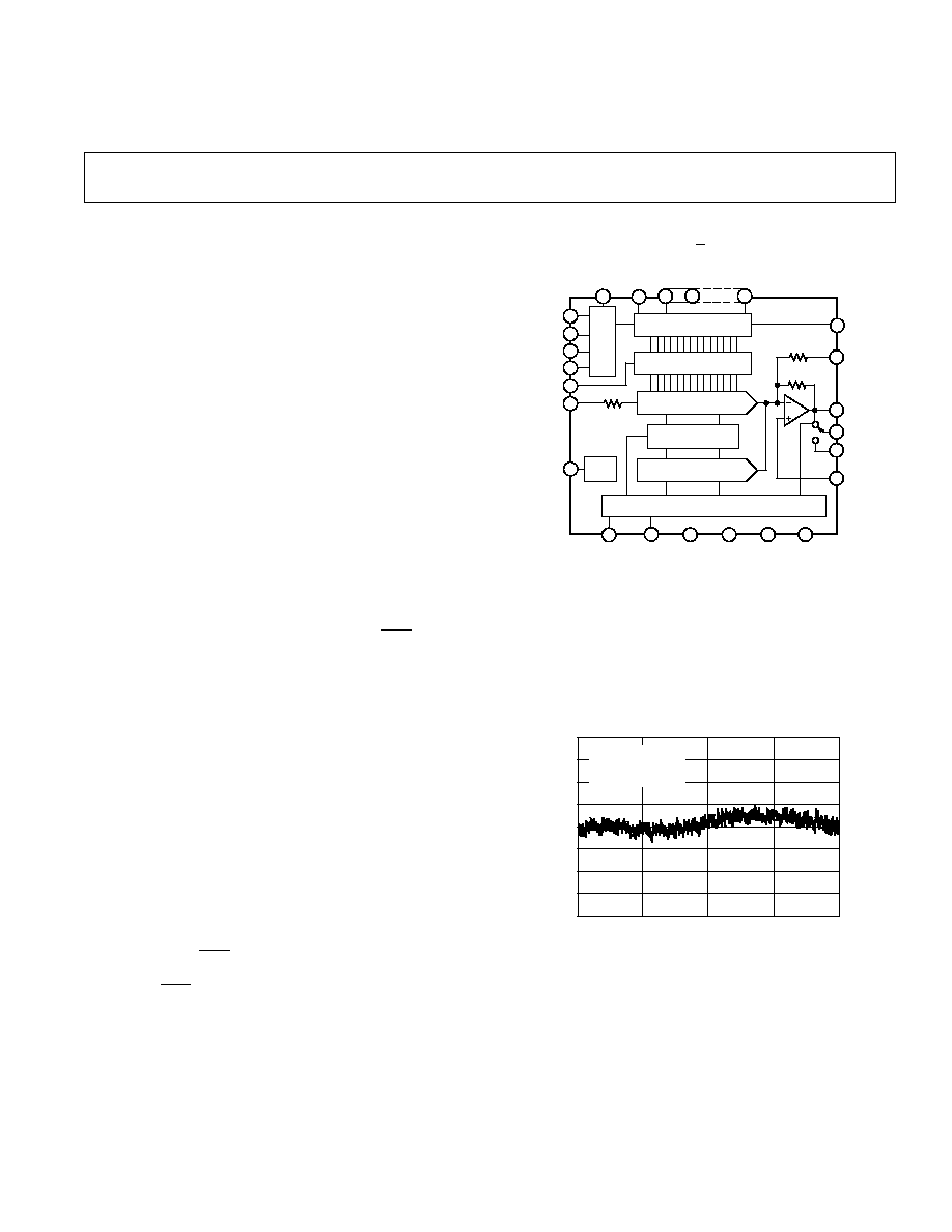
THEORY OF OPERATION
The AD760 uses autocalibration circuitry to produce a true
16-bit DAC with typically 0.2 LSB Integral and Differential
Linearity Error and 0.5 LSB Offset Error. The block diagram
in Figure 2 shows the circuit components needed for calibration.
The MAIN DAC uses an array of bipolar current sources with
MOS current steering switches to develop a current propor-
tional to the applied digital word, ranging from 0 mA to 2 mA.
A segmented architecture is used, where the most significant
four data bits are thermometer decoded to drive 15 equal cur-
rent sources. The lesser bits are scaled using an R-2R ladder,
then applied together with the segmented sources to the sum-
ming node of the output amplifier. An extra LSB is included in
the MAIN DAC, for use during calibration.
The self-calibration architecture of the AD760 attempts to
reduce the linearity errors of its transfer function. The algorithm
first checks for bipolar or unipolar operation, calibrates either
bipolar zero or unipolar offset, and then removes the carry er-
rors (DNL errors) associated with the upper 6 bits (64 codes).
Once calibrated, the top six bits of a code entering the MAIN
DAC simultaneously address the RAM, calling up a correction
code that is then applied to the CALDAC. The output cur-
rents of both the MAIN DAC and CALDAC are combined in
the summing amplifier to produce the corrected output voltage.
+10V
REF
10k
S
OUT
SPAN/
BIP
OFF
V
OUT
9.95k
LDAC
REF IN
REF OUT
HBE
SER
CLR
10k
AD760
UNI
/
BIP CLR
OR
LBE
MUX
OUT
MUX
I N
AGND
S
IN
OR
DB0
DB2
DB7
CS
MSB/
LSB
OR
DB1
12
18/16
SERIAL
OR
24
23
15
27
28
22
25
17
18
20
21
19
MAIN DAC
CONTROL
LOGIC
16
26
RAM
CALIBRATION SEQUENCER
CALOK
V
EE
+V
CC
+V
LL
DGND
CAL
1
2
3
5
6
4
14
16/18-BIT
INPUT REGISTER
13
7
CALIBRATION DAC
16/18-BIT DAC LATCH
TRANSFER STD DAC
Figure 2. Functional Block Diagram
In the first step of DNL calibration the output of the MAIN
DAC is set to the code just below the code to be calibrated.
The extra LSB in the MAIN DAC is turned on to find the ex-
trapolated value for the next code. The comparator is then
nulled using TRANSFER STD DAC. The voltage at V
OUT
has in effect been sampled at the code to be calibrated.
Next, the extra LSB is turned off and the MAIN DAC code is
incremented by one LSB. The comparator is once again
nulled, this time with the CALDAC, until the V
OUT
is adjusted
to equal the previously sampled output. The CALDAC code is
stored in RAM and the process is repeated for the next code.
DEFINITIONS OF SPECIFICATIONS
INTEGRAL NONLINEARITY: Analog Devices defines inte-
gral nonlinearity as the maximum deviation of the actual, ad-
justed DAC output from the ideal analog output (a straight line
drawn from 0 to FS 1 LSB) for any bit combination. This is
also referred to as relative accuracy.
DIFFERENTIAL NONLINEARITY: Differential nonlinearity
is the measure of the change in the analog output, normalized to
full scale, associated with a 1 LSB change in the digital input
code. Monotonic behavior requires that the differential linearity
error be greater than or equal to 1 LSB over the temperature
range of interest.
MONOTONICITY: A DAC is monotonic if the output either
increases or remains constant for increasing digital inputs with
the result that the output will always be a single-valued function
of the input.
GAIN ERROR: Gain error is a measure of the output error be-
tween an ideal DAC and the actual device output with all 1s
loaded after offset error has been adjusted out.
OFFSET ERROR: Offset error is a combination of the offset
errors of the voltage-mode DAC and the output amplifier and is
measured with all 0s loaded in the DAC.
BIPOLAR ZERO ERROR: When the AD760 is connected for
bipolar output and 10 . . . 000 is loaded in the DAC, the devia-
tion of the analog output from the ideal midscale value of 0 V is
called the bipolar zero error.
DRIFT: Drift is the change in a parameter (such as gain, offset
and bipolar zero) over a specified temperature range. The drift
temperature coefficient, specified in ppm/°C, is calculated by
measuring the parameter at T
MIN
, 25°C and T
MAX
and dividing
the change in the parameter by the corresponding temperature
change.
TOTAL HARMONIC DISTORTION + NOISE: Total har-
monic distortion + noise (THD+N) is defined as the ratio of the
square root of the sum of the squares of the values of the har-
monics and noise to the value of the fundamental input fre-
quency. It is usually expressed in percent (%). THD+N is a
measure of the magnitude and distribution of linearity error, dif-
ferential linearity error, quantization error and noise. The distri-
bution of these errors may be different, depending upon the
amplitude of the output signal. Therefore, to be the most useful,
THD+N should be specified for both large and small signal am-
plitudes.
SIGNAL-TO-NOISE RATIO: The signal-to-noise ratio is
defined as the ratio of the amplitude of the output when a full-
scale signal is present to the output with no signal present. This
is measured in dB.
DIGITAL-TO-ANALOG GLITCH IMPULSE: This is the
amount of charge injected from the digital inputs to the analog
output when the inputs change state. This is measured at half
scale when the DAC switches around the MSB and as many as
possible switches change state, i.e., from 011 . . . 111 to
100 . . . 000.
DIGITAL FEEDTHROUGH: When the DAC is not selected
(i.e., CS is held high), high frequency logic activity on the digi-
tal inputs is capacitively coupled through the device to show up
as noise on the V
OUT
pin. This noise is digital feedthrough.
AD760
REV. A
7
CALIBRATED LINEARITY PERFORMANCE
The cumulative probability plots for the AD760 INL and DNL
shown in Figures 3 and 4 represent the maximum absolute-
value (peak) linearity error for each part. Roughly 100 parts
from each of 3 wafer lots were used.
The calibrated DNL and INL performance for the sample
populations shown also represent the expected performance for
a single part calibrated often. There is essentially no difference
between the expected performance of many parts calibrated
once and one part calibrated often. The AD760 calibrated per-
formance is guaranteed at any temperature within the operating
temperature range. The peak nonlinearity for the sample popu-
lations shown are also representative of the expected maximum
linearity errors of a single part recalibrated at temperature.
40
30
20
10
0
40
20
0
60
80
100
CUMULATIVE PROBABILITY %
COUNT
0
0.125
0.25
0.375
0.5
0.625
0.75
16-BIT LSB
Figure 3. AD760 Peak INL
40
30
20
10
0
40
20
0
60
80
100
CUMULATIVE PROBABILITY %
COUNT
0
0.125
0.25
0.375
0.5
16-BIT LSB
50
Figure 4. AD760 Peak DNL
ANALOG CIRCUIT CONNECTIONS
Internal scaling resistors provided in the AD760 may be con-
nected to produce a unipolar output range of 0 V to +10 V or a
bipolar output range of 10 V to +10 V. Gain and offset drift
are minimized in the AD760 because of the thermal tracking of
the scaling resistors with other device components.
UNIPOLAR CONFIGURATION
The configuration shown in Figure 5a will provide a unipolar
0 V to +10 V output range. In this mode a 50 resistor is tied
between REF OUT (Pin 26) and REF IN (Pin 25). It is pos-
sible to use the AD760 without any external components by
tying Pin 26 directly to Pin 25. Eliminating this resistor will
increase the gain error by 0.50% of FSR.
SPAN/BIP OFF
V
OUT
23
24
+10V REF
25
MAIN DAC
REFOUT
26
REFIN
50
10k
10k
9.95k
AD760
Figure 5a. 0 V to +10 V Unipolar Voltage Output
If it is desired to adjust the gain error to zero, this can be ac-
complished using the circuit shown in Figure 5b. The adjust-
ment procedure is as follows:
STEP 1 . . . OFFSET ADJUST
Initiate calibration sequence. CALOK (Pin 1) must remain high
throughout Gain Adjust.
STEP 2 . . . GAIN ADJUST
Turn all bits ON and adjust gain trimmer, R1, until the output
is 9.999847 volts. (Full scale is adjusted to 1 LSB less than the
nominal full scale of 10.000000 volts.)
SPAN/BIP OFF
V
OUT
23
24
+10V REF
25
MAIN DAC
REFOUT
26
REFI N
R1
100
10k
10k
9.95k
AD760
Figure 5b. 0 V to +10 V Unipolar Voltage Output with
Gain Adjust
BIPOLAR CONFIGURATION
The circuit shown in Figure 6a will provide a bipolar output
voltage from 10.000000 V to +9.999694 V with positive full
scale occurring with all bits ON. As in the unipolar mode, resis-
tor R1 may be eliminated altogether to provide AD760 bipolar
operation without any external components. Eliminating this
resistor will increase the gain error by 0.50% of FSR in the
bipolar mode.
8
AD760
REV. A
SPAN/
BIP OFF
V
OUT
23
24
25
MAIN DAC
REFOUT
26
REFI N
R1
50
10k
10k
9.95k
AD760
+10V REF
Figure 6a. 0 V to ±10 V Bipolar Voltage Output
Gain Error can be adjusted to zero using the circuit shown in
Figure 6b. Note that gain adjustment changes the Bipolar Zero
by one half of the variation made to the full-scale output value.
Therefore, to eliminate iterating between Zero (calibration) and
Gain adjustment the following procedure is recommended.
STEP 1 . . . ZERO ADJUST
Initiate Calibration Sequence.
STEP 2 . . . GAIN ADJUST
Insure the CALOK pin remains high throughout the gain ad-
justment process. Turn all bits on and measure the output error
relative to the full-scale output of 9.99695 V. Adjust R1 until
the output is minus two times the full-scale output error. For
example, if the output error is 1 mV, adjust the output 2 mV
higher than the previous full-scale error.
STEP 3 . . . ZERO ADJUST
Initiate Calibration Sequence. The AD760 will calibrate Bipolar
Zero and the resulting Gain Error will be very small. Reload the
DAC with all ones to check the full-scale output error.
SPAN/
BIP OFF
V
OUT
23
24
+10V REF
25
MAIN DAC
REFOUT
26
REFI N
R1
100
10k
10k
9.95k
AD760
Figure 6b. 0 V to ±10 V Bipolar Voltage Output Gain
Adjustment
It should be noted that using external resistors will introduce a
small temperature drift component beyond that inherent in the
AD760. The internal resistors are trimmed to ratio-match and
temperature-track other resistors on chip, even though their
absolute tolerances are ±20% and absolute temperature coeffi-
cients are approximately 50 ppm/°C. In the case that external
resistors are used, the temperature coefficient mismatch be-
tween internal and external resistors, multiplied by the sensitiv-
ity of the circuit to variations in the external resistor value, will
be the resultant additional temperature drift.
INTERNAL/EXTERNAL REFERENCE USE
The AD760 has an internal low noise buried Zener diode refer-
ence that is trimmed for absolute accuracy and temperature co-
efficient. This reference is buffered and optimized for use in a
high speed DAC and will give long-term stability equal or supe-
rior to the best discrete Zener diode references. The perfor-
mance of the AD760 is specified with the internal reference
driving the DAC and with the DAC alone (for use with a preci-
sion external reference).
The internal reference has sufficient buffering to drive external
circuitry in addition to the reference currents required for the
DAC (typically 1 mA to REF IN and 1 mA to BIPOLAR OFF-
SET). A minimum of 2 mA is available for driving external
loads. The AD760 reference output should be buffered with an
external op amp if it is required to supply more than 4 mA total
current. The reference is tested and guaranteed to ±0.1% max
error.
It is also possible to use external references other than 10 volts
with slightly degraded linearity specifications. The recom-
mended range of reference voltages is +5 V to +10.24 V. For
example, by using the AD586 5 V reference, outputs of 0 V to
+5 V or ±5 V can be realized. Using the AD586 voltage refer-
ence makes it possible to operate the AD760 with ±12 V sup-
plies with 10% tolerances.
Figure 7 shows the AD760 using the AD586 precision 5 V refer-
ence in the bipolar configuration. The highest grade AD586MN
is specified with a drift of 2 ppm/°C. This circuit includes an
optional potentiometer that can be used to adjust the gain error
in a manner similar to that described in the Bipolar Configura-
tion section. Use +4.999847 V as the full-scale output value.
The AD760 can also be used with the AD587, 10 V reference,
using the same configuration shown in Figure 7 to produce a
±10 V output. The highest grade AD587L is specified at
5 ppm/°C.
SPAN/BIP OFF
V
OUT
23
24
+10V REF
25
MAIN DAC
REFOUT
26
REFI N
100
10k
10k
9.95k
AD760
AD586
2
4
6
V
OUT
+V
CC
Figure 7. Using the AD760 with the AD586 5 V Reference
OUTPUT SETTLING AND GLITCH
The AD760's output buffer amplifier typically settles to within
0.0008% FS (1/2 LSB) of its final value in 8 µs for a full-scale
step. Figures 8a and 8b show settling for a full scale and an
LSB step, respectively, with a 2 k , 1000 pF load applied. The
guaranteed maximum settling time at +25°C for a full-scale step
is 13 µs with this load. The typical settling time for a 1 LSB step
is 2.5 µs.
AD760
REV. A
9
The digital-to-analog glitch impulse is specified as 15 nV-s typi-
cal. Figure 8c shows the typical glitch impulse characteristic at
the code 011 . . . 111 to 100 . . . 000 transition when loading
the second rank register from the first rank register.
a. 10 V to +10 V Full-Scale Step Settling
b. LSB Step Settling
c. D-to-A Glitch Impulse
Figure 8. Output Characteristics
DIGITAL CIRCUIT DETAILS
The AD760 has several "dual-use" pins that allow flexible op-
eration while maintaining the lowest possible pin count and con-
sequently the smallest package size. The following information
is useful when applying the AD760.
The AD760 uses an internal Output Multiplexer to discon-
nect the DAC output from MUX
OUT
(Pin 27) when the device
is uncalibrated or when a calibration sequence is in progress. At
those times MUX
OUT
is switched to MUX
IN
(Pin 28) so the
user can force a predetermined output voltage. Refer to the fol-
lowing section for using the output multiplexer.
A Power-On-Reset feature senses whenever any power supply
is low enough to jeopardize the integrity of the calibration data
in the RAM. At power-up or in the event of a power supply
transient, CALOK (Pin 1) is low and the MUX
OUT
pin is
switched to MUX
IN
.
Self-Calibration
is initiated by strobing the CAL pin low (refer
to Figure 1d). The CALOK pin will go low and the MUX
OUT
pin is connected to MUX
IN
. During calibration, the second-rank
latch is transparent to allow the CALIBRATION SEQUENCER
to control the MAIN DAC. After successful completion of cali-
bration, the input to the second-rank latch is switched to the
first-rank latch, the DAC is loaded with the contents of the first-
rank latch, V
OUT
settles to the value represented by the data in
the first-rank latch, then CALOK will go high, and MUX
OUT
is
switched to V
OUT
. Therefore the user should program the DAC
with the desired data before initiating the calibration. The sec-
ond rank latch, controlled by LDAC, is a transparent latch. As
long as LDAC remains high, changes in the first rank latch will
be reflected in the DAC output immediately.
The status of the calibration may be determined by taking the
HBE
pin low. CALOK either switches high if the calibration is
in progress, or CALOK remains low if a power supply voltage
transient has interrupted the calibration and caused the AD760
to be set to the uncalibrated state.
When CLR is strobed, Pin 17 functions as a control input, UNI/
BIP CLR, that determines how the Asynchronous Clear func-
tion works (refer to Figure 1c). If the UNI/BIP CLR pin is a
logic low when CLR is strobed the DAC is set to minus full-
scale; a logic high sets the DAC to midscale. It should be noted
that the clear function clears the DAC Latch but does not clear
the first rank latch. Therefore, the data that remains in the first
rank latch can be reloaded by simply bringing LDAC high
again. Alternately, new data can be loaded into the first rank
latch if desired.
Serial Mode Operation
is enabled by bringing the SER (Pin
19) low. This changes the function of DB0 (Pin 14) to that of
the serial input pin, SIN. The function of DB1 (Pin 13) also
changes to a control input, MSB/LSB that determines which bit
is to be loaded first.
Sixteen or Eighteen-Bit Operation
is selected with another
dual use pin. DB2 (Pin 12) changes to a control input, 18/16-
SERIAL, that selects whether 16-bit or 18-bit serial data is to be
used. For 16-bit operation the data inputs, Pins 712, should be
tied low. For 18-bit operation Pin 12 must be tied high.
Data is clocked into the input shift register on the rising edge of
CS
as shown in Figure 1b. The data is then resident in the first
rank latch and can be loaded into the DAC by taking the LDAC
pin high. This will cause the DAC to change to the appropriate
output value. In serial mode the byte controls HBE (Pin 18)
and LBE (Pin 17) are disabled. Pin 17 can be tied to a logic
high or low depending on how the user wants the asynchronous
clear function to work. The Serial Out pin (S
OUT
) can be used
to daisy chain several DACs together in multi-DAC applications
to minimize the number of control lines required. The first rank
latch simply acts as a shift register, and repeated strobing of CS
will shift the data out through S
OUT
and into the next DAC.
Each DAC in the chain will require its own LDAC signal unless
all of the DACs are to be updated simultaneously.
5
0
0
600
400
200
200
400
600
µs
µV
1
2
3
4
5
0
0
+20
20
µs
mV
1
2
3
4
20
10
0
0
+10
10
600
400
200
0
200
400
600
VOLTS
µs
µV
10
AD760
REV. A
Byte Mode Operation
is enabled by setting SER high, which
configures DB0DB7 as data inputs. In this mode HBE and
LBE
are used to identify the data as either the high byte or the
low byte of the 16-bit word. The user can load the data in either
order into the first rank latch using the rising edge of the CS
signal as shown in Figure 1a. The status of Pin 17 when CLR is
strobed determines whether the AD760 clears to unipolar or
bipolar zero. (But it cannot be hardwired to the desired state, as
in the serial mode.)
NOTE: CS is edge triggered. HBE, LBE, CLR, SER, CAL, and
LDAC are level triggered.
USING THE OUTPUT MULTIPLEXER
The onboard multiplexer allows the user to isolate the load from
the voltage variations at V
OUT
during calibration. To minimize
the glitch-impulse at MUX
OUT
, the multiplexer input, MUX
IN
,
should be tied to a voltage equal to the DAC's negative
full-scale voltage. Since the DAC is loaded with the contents of
its first-rank latch before completing calibration, the DAC
should be programmed to negative full scale before calibrating.
This will minimize the voltage excursions of MUX
OUT
at the
beginning and end of calibration. If the glitch-impulse at the
beginning of calibration is not important, yet the user wants to
minimize the recovery time at MUX
OUT
, MUX
IN
should be set
to the voltage that corresponds to the data in the first-rank latch
before calibration is initiated.
The multiplexer series on-resistance limits its load-drive capability.
To attain 16-bit linearity, MUX
OUT
must be buffered with a
suitable op amp. The amplifier open loop-gain and common-
mode rejection contribute to gain error whereas the linearity of
these parameters affect the relative accuracy (or integral nonlin-
earity). In general, the amplifier linearity is not specified so its
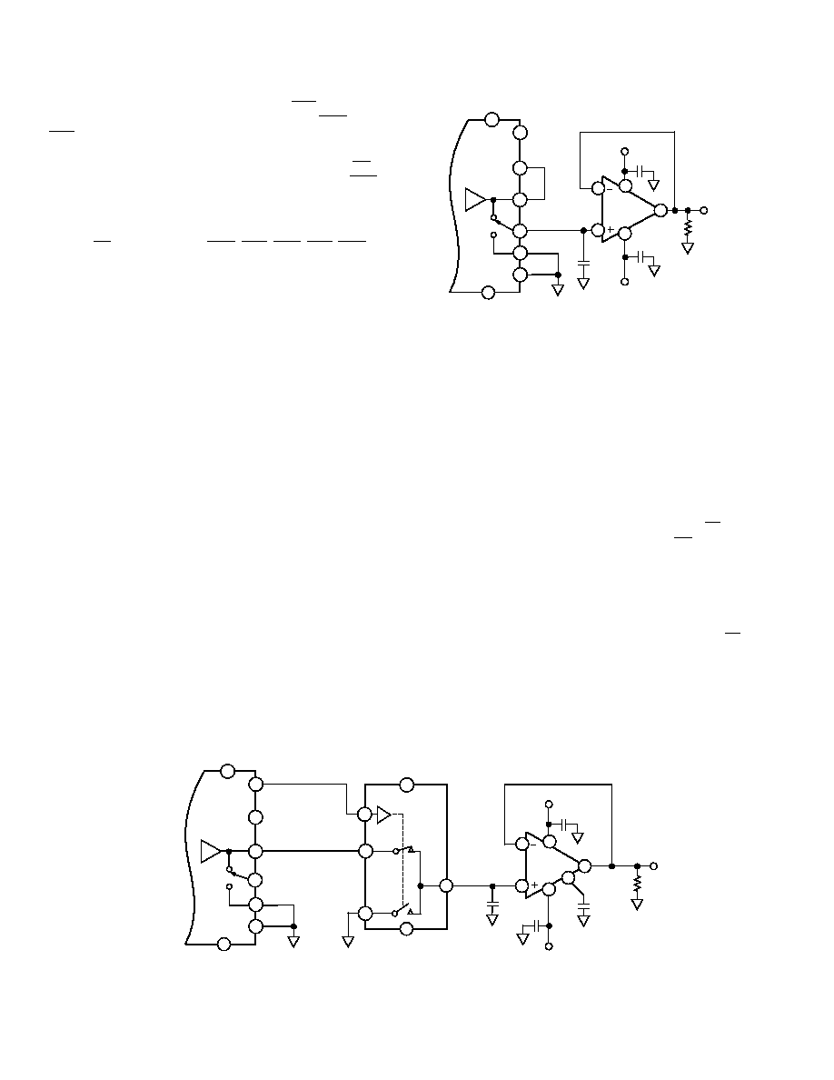
effects must be determined empirically. Using the AD707, as
shown in Figure 9, the overall linearity error is within 0.5 LSB.
The AD707C/T initial voltage offset and its temperature coeffi-
cient will not contribute more than 0.1 LSB to the Bipolar Zero
Error over the entire operating temperature range. The settling
time to 1/2 LSB is typically 100 µs for a 20 V step. For applica-
tions that require faster settling, the AD820 can be used to
attain full-scale settling to within a 1/2 LSB in 20 µs. The addi-
tional linearity error from the AD820 will be no more than
0.25 LSB.
100pF
+V
CC
0.1µF
OUTPUT
AD707
OR
AD820
2
7
6
3
4
MUX
O UT
22
23
28
27
1
4
MUX
I N
AGND
V
OUT
24
3
SPAN/
BIP OFF
CALOK
+V
CC
1k
0.1µF
AD760
V
EE
V
EE
Figure 9. Buffering the AD760 Internal MUX
USING AN EXTERNAL MULTIPLEXER
An external multiplexer like the ADG419 allows the user to
minimize the glitch impulse when holding the output to any
predetermined voltage during calibration. The ADG419 can be
used with a high speed op amp like the AD829, as shown in Fig-
ure 10, to attain the fastest possible settling time while main-
taining 16-bit linearity. The settling time to 1/2 LSB for a 20 V
step is typically 10 µs.
AD760 TO MC68HC11 (SPI* BUS) INTERFACE
The AD760 interface to the Motorola SPI (serial peripheral in-
terface) is shown in Figure 11. The MOSI, SCK, and SS pins of
the HC11 are respectively connected to the S
IN
, CS and LDAC
pins of the AD760. The majority of the interfacing issues are
taken care of in the software initialization. A typical routine such
as the one shown below begins by initializing the state of the
various SPI data and control registers.
The most significant data byte (MSBY) is then retrieved from
memory and processed by the SENDAT subroutine. The SS
pin is driven low by indexing into the PORTD data register and
clearing Bit 5. The MSBY is then sent to the SPI data
register where it is automatically transferred to the AD760.
*SPI is a registered trademark of Motorola.
MUX
OUT
22
23
28
1
4
MUX
I N
AGND
V
OUT
24
3
SPAN/
BIP OFF
CALOK
+V
CC
AD760
V
EE
1nF
+V
CC
0.1µF
OUT
2
7
6
3
4
1k
0.1µF
V
EE
60pF
ADG419
8
2
1
6
27
5
4
+V
CC
7
V
EE
AD829
Figure 10. Using the AD760 with an External MUX
AD760
REV. A
11
The HC11 generates the requisite 8 clock pulses with data valid
on the rising edges. After the most significant byte is transmit-
ted, the least significant byte (LSBY) is loaded from memory
and transmitted in a similar fashion. To complete the transfer,
the LDAC pin is driven high latching the complete 16-bit word
into the AD760.
I
NIT
LDAA
#$2F
;SS = 1; SCK = 0; MOSI = I
STAA
PORTD
;SEND TO SPI OUTPUTS
LDAA
#$38
;SS
, SCK,MOSI = OUTPUTS
STAA
DDRD
;SEND DATA DIRECTION INFO
LDAA
#$50
;DABL INTRPTS,SPI IS MASTER & ON
STAA
SPCR
;CPOL=0, CPHA=0,1MHZ BAUD RATE
NEXTPT LDAA
MSBY
;LOAD ACCUM W/UPPER 8 BITS
BSR
SENDAT ;JUMP TO DAC OUTPUT ROUTINE
JMP
NEXTPT ;INFINITE LOOP
SENDAT LDY
#$1000
;POINT AT ON-CHIP REGISTERS
BCLR
$08,Y,$20 ;DRIVE SS (LDAC) LOW
STAA
SPDR
;SEND MS-BYTE TO SPI DATA REG
WAIT1
LDAA
SPSR
;CHECK STATUE OF SPIE
BPL
WAIT1
;POLL FOR END OF X-MISSION
LDAA
LSBY
;GET LOW 8 BITS FROM MEMORY
STAA
SPDR
;SEND LS-BYTE TO SPI DATA REG
WAIT2
LDAA
SPSR
;CHECK STATUS OF SPIE
BPL
WAIT2
;POLL FOR END OF X-MISSION
BSET
$08,Y,$20 ;DRIV SS HIGH TO LATCH DATA
RTS
MOSI
68HC11
SS
S
IN
LDAC
SER
AD760
SCK
CS
Figure 11. AD760 to 68HC11 (SPI) Interface
AD760 TO MICROWIRE INTERFACE
The flexible serial interface of the AD760 is also compatible
with the National Semiconductor MICROWIRE* interface.
The MICROWIRE* interface is used on microcontrollers such
as the COP400 and COP800 series of processors. A generic in-
terface to the MICROWIRE interface is shown in Figure 12.
The G1, SK, and SO pins of the MICROWIRE interface are re-
spectively connected to the LDAC, CS and S
IN
pins of the
AD760.
S
IN
LDAC
SER
AD760
SO
SK
MICROWIRE
CS
G1
Figure 12. AD760 to MICROWIRE Interface
NOISE
In high resolution systems, noise is often the limiting factor. A
16-bit DAC with a 10 volt span has an LSB size of 153 µV
(96 dB). Therefore, the noise must remain below this level in
*MICROWIRE is a registered trademark of National Semiconductor.
the frequency range of interest. The AD760's noise spectral
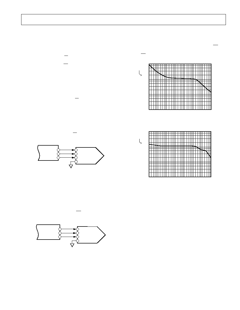
density is shown in Figures 13 and 14. Figure 13 shows the
DAC output noise voltage spectral density for a 20 V span ex-
cluding the reference. This figure shows the l/f corner frequency
at 100 Hz and the wideband noise to be below 120 nV/ Hz.
Figure 14 shows the reference wideband noise to be below
125 nV/ Hz.
1000
1
1
1M
100
10
10
100k
10k
1k
100
10M
FREQUENCY Hz
NOISE VOLTAGE nV/ Hz
Figure 13. DAC Output Noise Voltage Spectral Density
1000
1
1
1M
100
10
10
100k
10k
1k
100
10M
FREQUENCY Hz
NOISE VOLTAGE nV/ Hz
Figure 14. Reference Noise Voltage Spectral Density
BOARD LAYOUT
Designing with high resolution data converters requires careful
attention to board layout. Trace impedance is the first issue. A
306 µA current through a 0.5 trace will develop a voltage
drop of 153 µV, which is 1 LSB at the 16-bit level for a 10 V
full-scale span. In addition to ground drops, inductive and ca-
pacitive coupling need to be considered, especially when high
accuracy analog signals share the same board with digital sig-
nals. Finally, power supplies need to be decoupled in order to
filter out ac noise.
Analog and digital signals should not share a common path.
Each signal should have an appropriate analog or digital return
routed close to it. Using this approach, signal loops enclose a
small area, minimizing the inductive coupling of noise. Wide PC
tracks, large gauge wire, and ground planes are highly recom-
mended to provide low impedance signal paths. Separate analog
and digital ground planes should also be used, with a single in-
terconnection point to minimize ground loops. Analog signals
should be routed as far as possible from digital signals and
should cross them at right angles.
12
AD760
REV. A
One feature that the AD760 incorporates to help the user layout
is that the analog pins (V
CC
, V
EE
, REF OUT, REF IN, SPAN/
BIP OFFSET, V
OUT
, MUX
OUT
, MUX
IN
and AGND) are adja-
cent to help isolate analog signals from digital signals.
SUPPLY DECOUPLING
The AD760 power supplies should be well filtered, well regu-
lated, and free from high frequency noise. Switching power sup-
plies are not recommended due to their tendency to generate
spikes which can induce noise in the analog system.
Decoupling capacitors should be used in very close layout prox-
imity between all power supply pins and ground. A 10 µF tantalum
capacitor in parallel with a 0.1 µF ceramic capacitor provides ad-
equate decoupling. V
CC
and V
EE
should be bypassed to analog
ground, while V
LL
should be decoupled to digital ground.
An effort should be made to minimize the trace length between
the capacitor leads and the respective converter power supply
and common pins. The circuit layout should attempt to locate
the AD760, associated analog circuitry and interconnections as
far as possible from logic circuitry. A solid analog ground plane
around the AD760 will isolate large switching ground currents.
For these reasons, the use of wire wrap circuit construction is not
recommended; careful printed circuit construction is preferred.
GROUNDING
The AD760 has two pins, designated analog ground (AGND)
and digital ground (DGND.) The analog ground pin is the
"high quality" ground reference point for the device. Any exter-
nal loads on the output of the AD760 should be returned to
analog ground. If an external reference is used, this should also
be returned to the analog ground.
If a single AD760 is used with separate analog and digital
ground planes, connect the analog ground plane to AGND and
the digital ground plane to DGND keeping lead lengths as short
as possible. Then connect AGND and DGND together at the
AD760. If multiple AD760s are used or the AD760 shares ana-
log supplies with other components, connect the analog and
digital returns together once at the power supplies rather than at
each chip. This single interconnection of grounds prevents large
ground loops and consequently prevents digital currents from
flowing through the analog ground.
PRINTED IN U.S.A.
C2023184/95
PACKAGE INFORMATION
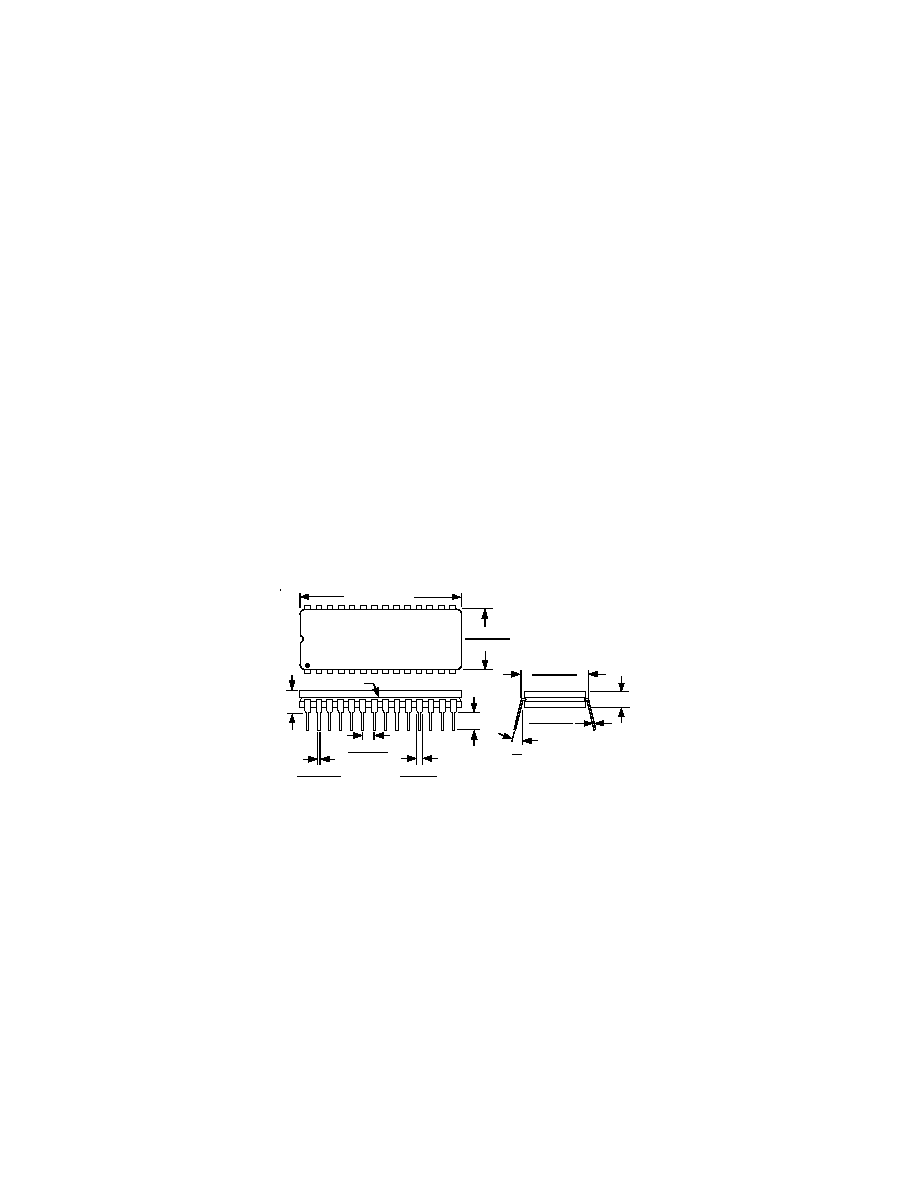
28-Pin Cerdip Package (Q-28)
1.490 (37.84) MAX
28
1
15
14
GLASS SEALANT
0.18 (4.57)
MAX
0.620 (15.74)
0.590 (14.93)
15
°
0
°
0.012 (0.305)
0.008 (0.203)
0.125 (3.175)
MIN
0.02 (0.5)
0.016 (0.406)
0.06 (1.52)
0.05 (1.27)
0.11 (2.79)
0.099 (2.28)
0.22
(5.59)
MAX
0.525 (13.33)
0.515 (13.08)