 | ÐлекÑÑоннÑй компоненÑ: AD767 | СкаÑаÑÑ:  PDF PDF  ZIP ZIP |
Äîêóìåíòàöèÿ è îïèñàíèÿ www.docs.chipfind.ru
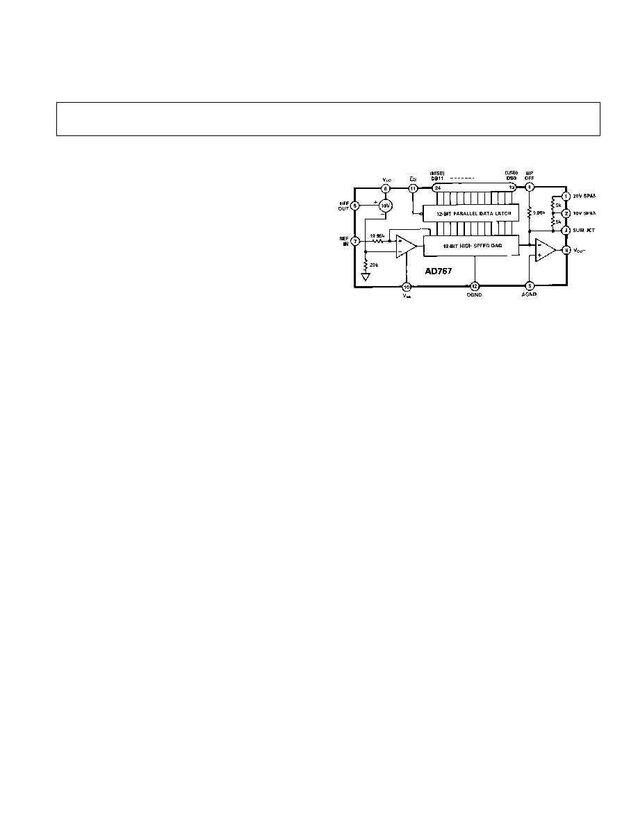
FUNCTIONAL BLOCK DIAGRAM
REV. A
Information furnished by Analog Devices is believed to be accurate and
reliable. However, no responsibility is assumed by Analog Devices for its
use, nor for any infringements of patents or other rights of third parties
which may result from its use. No license is granted by implication or
otherwise under any patent or patent rights of Analog Devices.
a
Microprocessor-Compatible
12-Bit D/A Converter
AD767*
PRODUCT DESCRIPTION
The AD767 is a complete voltage output 12-bit digital-to-
analog converter including a high stability buried Zener
reference and input latch on a single chip. The converter uses
12 precision high-speed bipolar current steering switches and a
laser-trimmed thin-film resistor network to provide high accuracy.
Microprocessor compatibility is achieved by the on-chip latch.
The design of the input latch allows direct interface to 12-bit
buses. The latch responds to strobe pulses as short as 40 ns,
allowing use with the fastest available microprocessors.
The functional completeness and high performance of the
AD767 result from a combination of advanced switch design,
high-speed bipolar manufacturing process, and the proven laser
wafer-trimming (LWT) technology.
The subsurface (buried) Zener diode on the chip provides a
low-noise voltage reference which has long-term stability and
temperature drift characteristics comparable to the best discrete
reference diodes. The laser trimming process which provides the
excellent linearity is also used to trim the absolute value of the
reference as well as its temperature coefficient. The AD767 is
thus well suited for wide temperature range performance with
±
1/2 LSB maximum linearity error and guaranteed monotonicity
over the full temperature range. Typical full-scale gain T.C. is
5 ppm/
°
C.
*Protected by Patent Numbers 3,803,590; 3,890,611; 3,932,863; 3,978,473;
4,020,486; and others pending.
FEATURES
Complete 12-Bit D/A Function
On-Chip Output Amplifier
High Stability Buried Zener Reference
Fast 40 ns Write Pulse
0.3" Skinny DIP and PLCC Packages
Single Chip Construction
Monotonicity Guaranteed Over Temperature
Settling Time: 3 s max to 1/2 LSB
Guaranteed for Operation with 12 V or 15 V Supplies
TTL/5 V CMOS Compatible Logic Inputs
MIL-STD-883 Compliant Versions Available
PRODUCT HIGHLIGHTS
1. The AD767 is a complete voltage output DAC with voltage
reference and digital latches on a single IC chip.
2. The input latch responds to write pulse widths as short as
40 ns assuring direct interface with the industry's fastest
microprocessors.
3. The internal buried Zener reference is laser-trimmed to
10.00 volts with a
±
1% maximum error. The reference
voltage is also available for external application.
4. The gain setting and bipolar offset resistors are matched to
the internal ladder network to guarantee a low gain temperature
coefficient and are laser trimmed for minimum full-scale and
bipolar offset errors.
5. The precision high-speed current steering switches and
on-board high-speed output amplifier settle within 1/2 LSB
for a 10 V full-scale transition in 3.0
µ
s when properly
compensated.
6. The AD767 is available in versions compliant with
MIL-STD-883. Refer to the Analog Devices Military
Products Databook or current AD767/883B data sheet for
detailed specifications.
One Technology Way, P.O. Box 9106, Norwood, MA 02062-9106, U.S.A.
Tel: 617/329-4700
Fax: 617/326-8703

REV. A
2
AD767SPECIFICATIONS
(T
A
= +25 C, 15 volt power supplies, Unipolar Mode, unless otherwise noted.)
Model
AD767J/A/S
1
AD767K/B
AD767A
2
Chips
Min
Typ
Max
Min
Typ
Max
Min
Typ
Max
Units
DIGITAL INPUTS
Resolution
12
12
12
Bits
Logic Levels (TTL Compatible, T
MIN
T
MAX
)
3
V
IH
(Logic "1")
+2.0
+5.5
+2.0
+5.5
+2.0
+5.5
V
V
IL
(Logic "0") J, K, A, B
0
+0.8
0
+0.8
0
+0.8
V
V
IL
(Logic "0") S
0
+0.7
V
I
IH
(V
IH
= 5.5 V)
3
10
3
10
3
10
µ
A
I
IL
(V
IL
= 0.8 V)
1
5
1
5
1
5
µ
A
TRANSFER CHARACTERISTICS
ACCURACY
Linearity Error @ +25
°
C
±
1/2
1
±
1/8
1/2
±
1/2
1
LSB
T
A
= T
MIN
to T
MAX
±
1/2
1
±
1/4
1/2
±
1/2
1
LSB
Differential Linearity Error @ +25
°
C
±
1/2
1
±
1/4
1
±
1/2
1
LSB
T
A
= T
MIN
to T
MAX
Monotonicity Guaranteed Monotonicity Guaranteed Monotonicity Guaranteed
LSB
Gain Error
4
±
0.1
0.2
±
0.1
0.2
±
0.1
0.2
% of FSR
5
Unipolar Offset Error
4
±
1
2
±
1
2
±
1
2
LSB
Bipolar Zero Error
4
±
0.05
0.1
±
0.05
0.1
±
0.05
0.1
% of FSR
DRIFT
Gain T
A
= 25
°
C to T
MIN
or T
MAX
±
5
±
30
±
5
±
15
±
5
±
30
ppm of FSR/
°
C
Unipolar Offset T
A
= 25
°
C to T
MIN
or T
MAX
±
1
±
3
±
1
±
3
±
1
±
3
ppm of FSR/
°
C
Bipolar Zero T
A
= 25
°
C to T
MIN
or T
MAX
±
5
±
10
±
10
±
5
±
10
ppm of FSR/
°
C
CONVERSION SPEED
Settling Time to
±
0.01% of FSR for
FSR change (2 k
||
500 pF load)
with 10 k
Feedback
3
4
3
4
3
4
µ
s
with 5 k
Feedback
2
3
2
3
2
3
µ
s
For LSB Change
1
1
1
µ
s
Slew Rate
10
10
10
V/
µ
s
ANALOG OUTPUT
Ranges
6
±
2.5,
±
5,
±
10,
±
2.5,
±
5,
±
10,
±
2.5,
±
5,
±
10,
V
+5, +10
+5, +10
+5, +10
Output Current
±
5
±
5
±
5
mA
Output Impedance (dc)
0.05
0.05
0.05
Short-Circuit Current
40
40
40
mA
REFERENCE OUTPUT
9.90
10.00
10.10
9.90
10.00
10.10
9.90
10.00
10.10
V
External Current
0.1
1.0
0.1
1.0
0.1
1.0
mA
POWER SUPPLY SENSITIVITY
V
CC
= +11.4 to +16.5 V dc
5
10
5
10
5
10
ppm of FS/%
V
EE
= 11.4 to 16.5 V dc
5
10
5
10
5
10
ppm of FS/%
POWER SUPPLY REQUIREMENTS
Rated Voltages
±
12,
±
15
±
12,
±
15
±
12,
±
15
V
Range
6
11.4
16.5
11.4
16.5
11.4
16.5
V
Supply Current
+11.4 to +16.5 V dc
9
13
9
13
9
13
mA
11.4 to 16.5 V dc
18
23
18
23
18
23
mA
Total Power Consumption
400
600
400
600
400
600
mW
TEMPERATURE RANGE
J/K
0
+70
0
+70
°
C
A/B
25
+85
25
+85
25
+85
°
C
S
55
+125
55
+125
°
C
Operating
55
+125
55
+125
°
C
Storage (All Grades)
65
+125
65
+125
65
+125
°
C
NOTES
1
AD767 "S" specifications shown for information only. Consult Analog Devices Military Databook or contact factory for a controlled specification sheet.
2
AD767A Chips specifications are tested at +25
°
C and, when in boldface, at +85
°
C. They are typical at 25
°
C.
3
The digital input specifications are 100% tested at +25
°
C, and guaranteed but not tested over the full temperature range.
4
Adjustable to zero.
5
FSR means "Full-Scale Range" and is 20 V for
±
10 V range and 10 V for the
±
5 V range.
6
A minimum power supply of
±
12.5 V is required for a
±
10 V full-scale output and
±
11.4 V is required for all other voltage ranges.
Specifications subject to change without notice.
Specifications shown in boldface are tested on all production units at final electrical test (except per Notes 1 and 2). Results from those tests are used to calculate
outgoing quality levels. All min and max specifications are guaranteed, although only those shown in boldface are tested on all production units.
AD767
REV. A
3
ABSOLUTE MAXIMUM RATINGS*
V
CC
to Power Ground . . . . . . . . . . . . . . . . . . . . .0 V to +18 V
V
EE
to Power Ground . . . . . . . . . . . . . . . . . . . . . 0 V to 18 V
Digital Inputs (Pins 11, 1324)
to Power Ground . . . . . . . . . . . . . . . . . . . . 1.0 V to +7.0 V
Ref In to Reference Ground . . . . . . . . . . . . . . . . . . . . . .
±
12 V
Bipolar Offset to Reference Ground . . . . . . . . . . . . . . . .
±
12 V
10 V Span R to Reference Ground . . . . . . . . . . . . . . . . .
±
12 V
20 V Span R to Reference Ground . . . . . . . . . . . . . . . . .
±
24 V
Ref Out, V
OUT
(Pins 6, 9) . . . Indefinite short to power ground
Momentary Short to V
CC
Power Dissipation . . . . . . . . . . . . . . . . . . . . . . . . . . . 1000 mW
*Stresses above those listed under "Absolute Maximum Ratings" may cause
permanent damage to the device. This is a stress rating only and functional
operation of the device at these or any other conditions above those indicated in
the operational sections of this specification is not implied. Exposure to absolute
maximum rating conditions for extended periods may affect device reliability.
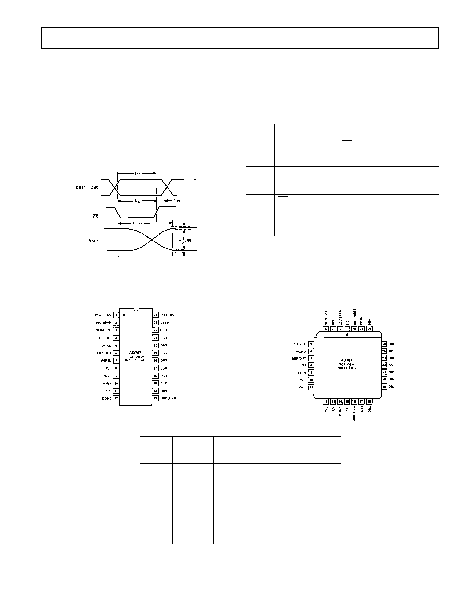
TIMING SPECIFICATIONS
(All Models, T
A
= 25
°
C, V
CC
= +12 V or +15 V,
V
EE
= 12 V or 15 V)
Symbol
Parameter
Min Typ Max
t
DS
Data Valid to End of CS
40
ns
(25
°
C to +85
°
C)
60
ns
(55
°
C to +125
°
C)
90
ns
t
DH
Data Hold Tiine
10
ns
(25
°
C to +85
°
C)
10
ns
(55
°
C to +125
°
C)
20
ns
t
CS
CS
Pulse Width
40
ns
(25
°
C to +85
°
C)
60
ns
(55
°
C to +125
°
C)
90
ns
t
SETT
Output Voltage Settling Time*
2
4
µ
s
*t
SETT
is measured referenced to the leading edge of t
CS
. If t
CS
> t
DS
, then
t
SETT
is measured referenced to the beginning of Data Valid.
PIN CONFIGURATION
PLCC
DIP
ORDERING GUIDE
Linearity
Gain T.C.
Temperature
Error Max
Max
Model
1
Package
Range C
T
MIN
T
MAX
ppm/ C
AD767JN
Plastic DIP
0 to +70
±
1 LSB
30
AD767JP
PLCC
0 to +70
±
1 LSB
30
AD767KN Plastic DIP
0 to +70
±
1/2 LSB
15
AD767KP
PLCC
0 to +70
±
1/2 LSB
15
AD767AD
Ceramic DIP
25 to +85
±
1 LSB
30
AD767BD
Ceramic DIP
25 to +85
±
1/2 LSB
15
AD767SD/
883B
Ceramic DIP
55 to +125
Note 2
Note 2
AD767A
Chips
N/A
25 to +85
±
1 LSB
30
NOTES
1
D = Ceramic DIP; N = Plastic DIP; P = Plastic Leaded Chip Carrier.
2
For details on grade and package offerings screened in accordance with MIL-STD-883, refer to
the Analog Devices Military Products Databook or current AD767/883B data sheet.
AD767
REV. A
4
THE AD767 OFFERS TRUE 12-BIT PERFORMANCE
OVER THE FULL TEMPERATURE RANGE
LINEARITY ERROR: Analog Devices defines linearity error as
the maximum deviation of the actual, adjusted DAC output
from the ideal analog output (a straight line drawn from 0 to
F.S. 1 LSB) for any bit combination. This is also referred to as
relative accuracy. The AD767 is laser trimmed to typically
maintain linearity errors at less than
±
1/8 LSB for the K and B
versions and
±
1/2 LSB for the J, A and S versions. Linearity
over temperature is also held to
±
1/2 LSB (K/B) or
±
1 LSB
(J/A/S).
MONOTONICITY: A DAC is said to be monotonic if the
output either increases or remains constant for increasing digital
inputs such that the output will always be a nondecreasing
function of input. All versions of the AD767 are monotonic over
their full operating temperature range.
DIFFERENTIAL NONLINEARITY: Monotonic behavior
requires that the differential linearity error be less than 1 LSB
both at +25
°
C as well as over the temperature range of interest.
Differential nonlinearity is the measure of the variation in analog
value, normalized to full scale, associated with a 1 LSB change
in digital input code. For example, for a 10 volt full-scale
output, a change of 1 LSB in digital input code should result in
a 2.44 mV change in the analog output (1 LSB = 10 V
1/4096 = 2.44 mV). If in actual use, however, a 1 LSB change
in the input code results in a change of only 0.61 mV (1/4 LSB)
in analog output, the differential nonlinearity error would be
1.83 mV, or 3/4 LSB.
GAIN ERROR: DAC gain error is a measure of the difference
between an ideal DAC and the actual device's output span. All
grades of the AD767 have a maximum gain error of 0.2% FS.
However, if this is not sufficient, the error can easily be adjusted
to zero (see Figures 2 and 3).
UNIPOLAR OFFSET ERROR: Unipolar offset error is a
combination of the offset errors of the voltage-mode DAC and
the output amplifier and is measured when the AD767 is
configured for unipolar outputs. It is present for all codes and is
measured with all "0s" in the DAC latches. This is easily
adjustable to zero when required.
BIPOLAR ZERO ERROR: Bipolar zero errors result from
errors produced by the DAC and output amplifier when the
AD767 is configured for bipolar output. Again, as with unipolar
offset and gain errors, this is easily adjusted to zero when
required.
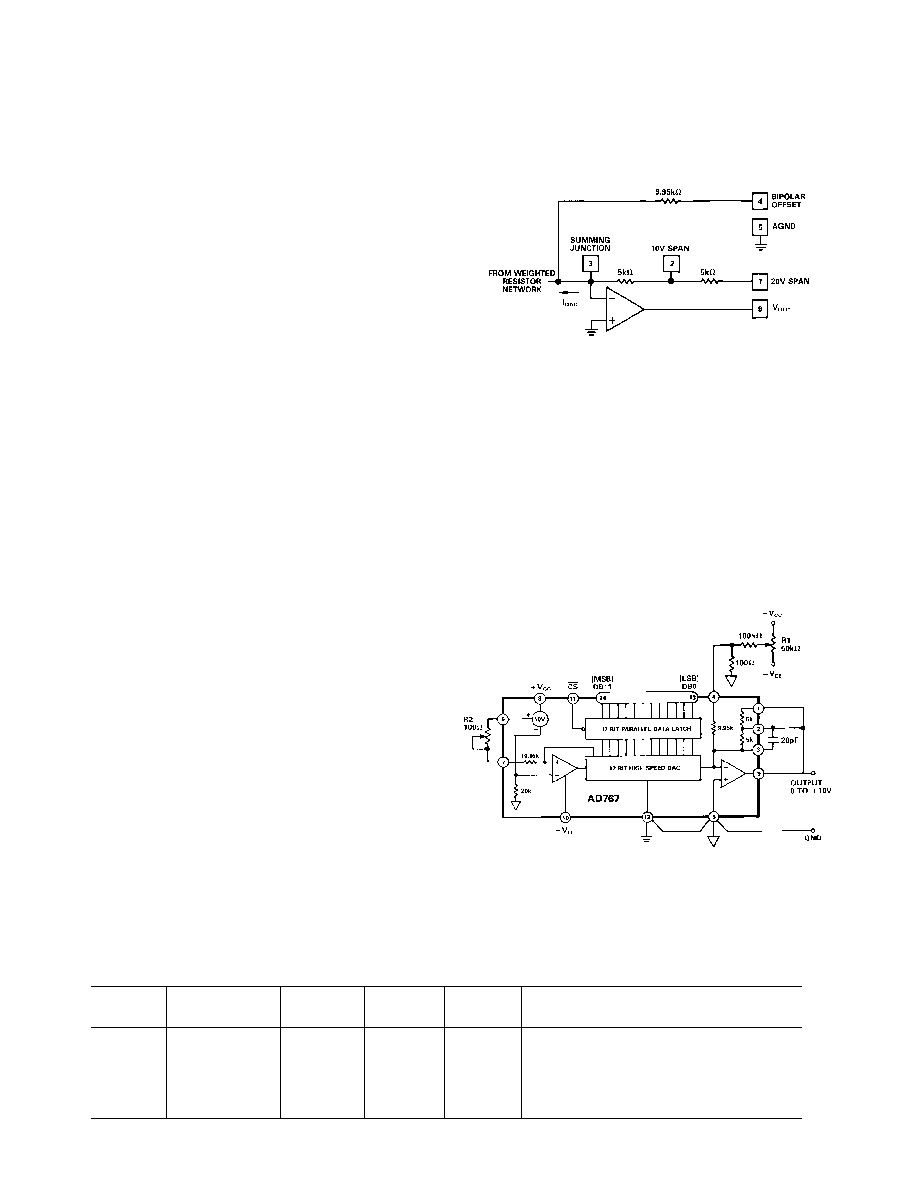
ANALOG CIRCUIT CONNECTIONS
Internal scaling resistors provided in the AD767 may be connected
to produce bipolar output voltage ranges of
±
10,
±
5 or
±
2.5 V
or unipolar output voltage ranges of 0 to +5 V or 0 to +10 V.
Gain and offset drift are minimized in the AD767 because of the
thermal tracking of the scaling resistors with other device
components. Connections for various output voltage ranges are
shown in Table I.
Figure 1. Output Amplifier Voltage Range Scaling Circuit
UNIPOLAR CONFIGURATION (Figure 2)
This configuration will provide a unipolar 0 to +10 volt output
range. In this mode, the bipolar offset terminal, Pin 4, should be
grounded if not used for trimming.
STEP I ... ZERO ADJUST
Turn all bits OFF and adjust zero trimmer R1, until the output
reads 0.000 volts (1 LSB = 2.44 mV). In most cases this trim is
not needed, and Pin 4 should be connected to Pin 5.
STEP II ... GAIN ADJUST
Turn all bits ON and adjust 100
gain trimmer R2 until the
output is 9.9976 volts. (Full scale is adjusted to 1 LSB less than
nominal full scale of 10.000 volts.)
Figure 2. 0 to +10 V Unipolar Voltage Output
Table I. Output Voltage Range Connections
Output
Digital
Connect
Connect
Connect
Connect
Range
Input Codes
Pin 9 to
Pin 1 to
Pin 2 to
Pin 4 to
±
10 V
Offset Binary
1
9
NC
6 (through 50
fixed or 100
trim resistor)
±
5 V
Offset Binary
1 and 2
2 and 9
1 and 9
6 (through 50
fixed or 100
trim resistor)
±
2.5 V
Offset Binary
2
3
9
6 (through 50
fixed or 100
trim resistor)
0 to +10 V
Straight Binary
1 and 2
2 and 9
1 and 9
5 (or optional trim See Figure 2)
0 to +5 V
Straight Binary
2
3
9
5 (or optional trim See Figure 2)
AD767
REV. A
5
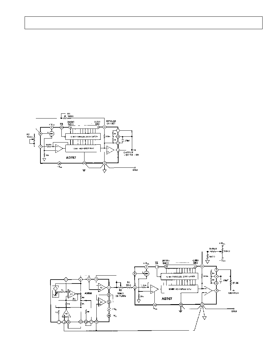
BIPOLAR CONFIGURATION (Figure 3)
This configuration will provide a bipolar output voltage from
5.000 to +4.9976 volts, with positive full scale occurring with
all bits ON (all 1s).
STEP I ... OFFSET ADJUST
Turn OFF all bits. Adjust 100
trimmer R1 to give 5.000
volts output.
STEP II ... GAIN ADJUST
Turn ON all bits. Adjust 100
gain trimmer R2 to give a
reading of +4.9976 volts.
STEP III ... BIPOLAR ZERO ADJUST (Optional)
In applications where an accurate zero output is required, set
the MSB ON, all other bits OFF, and readjust R1 for zero volts
output.
Figure 3.
±
5 V Bipolar Voltage Output
INTERNAL/EXTERNAL REFERENCE USE
The AD767 has an internal low-noise buried Zener diode
reference which is trimmed for absolute accuracy and tempera-
ture coefficient. This reference is buffered and optimized for use
in a high-speed DAC and will give long-term stability equal or
superior to the best discrete Zener reference diodes. The per-
formance of the AD767 is specified with the internal reference
driving the DAC since all trimming and testing (especially for
full-scale error and bipolar offset) is done in this configuration.
The internal reference has sufficient buffering to drive external
circuitry in addition to the reference currents required for the
DAC (typically 0.5 mA to Ref In and 1.0 mA to Bipolar Offset).
A minimum of 0.1 mA is available for driving external loads.
The AD767 reference output should be buffered with an
external op amp if it is required to supply more than 0.1 mA
output current. The reference is typically trimmed to
±
0.2%,
then tested and guaranteed to
±
1.0% max error. The
temperature coefficient is comparable to that of the full-scale
TC for a particular grade.
If an external reference is used (10.000 V, for example),
additional trim range must be provided, since the internal
reference has a tolerance of
±
1%, and the AD767 full-scale and
bipolar offset are both trimmed with the internal reference. The
gain and offset trim resistors give about
±
0.25% adjustment
range, which is sufficient for the AD767 when used with the
internal reference.
It is also possible to use external references other than 10 volts.
The recommended range of reference voltage is from +8 to
+10.5 volts, which allows both 8.192 V and 10.24 V ranges to
be used. The AD767 is optimized for fixed-reference applications.
If the reference voltage is expected to vary over a wide range in
a particular application, a CMOS multiplying DAC is a better
choice.
Reduced values of reference voltage will also permit the
±
12 volt
±
5% power supply requirement to be relaxed to
±
12 volts
±
10%.
It is not recommended that the AD767 be used with external
feedback resistors to modify the scale factor. The internal
resistors are trimmed to ratio-match and temperature-track the
other resistors on the chip, even though their absolute tolerances
are
±
20%, and absolute temperature coefficients are approximately
50 ppm/
°
C. If external resistors are used, a wide trim range
(
±
20%) will be needed and temperature drift will be increased
to reflect the mismatch between the temperature coefficients of
the internal and external resistors.
Small resistors may be added to the feedback resistors in order
to accomplish small modifications in the scaling. For example, if
a 10.24 V full scale is desired, a 140
1% low-TC metal-film
resistor can be added in series with the internal (nominal) 5k
feedback resistor, and the gain trim potentiometer (between
Pins 6 and 7) should be increased to 200
. In the bipolar
mode, increase the value of the bipolar offset trim potentiometer
also to 200
.
Figure 4. Using the AD767 with the AD588 High Precision Reference