 | ÐлекÑÑоннÑй компоненÑ: AD7701 | СкаÑаÑÑ:  PDF PDF  ZIP ZIP |
Äîêóìåíòàöèÿ è îïèñàíèÿ www.docs.chipfind.ru
REV. D
Information furnished by Analog Devices is believed to be accurate and
reliable. However, no responsibility is assumed by Analog Devices for its
use, nor for any infringements of patents or other rights of third parties
which may result from its use. No license is granted by implication or
otherwise under any patent or patent rights of Analog Devices.
a
AD7701
LC
2
MOS
16-Bit A/D Converter
FEATURES
Monolithic 16-Bit ADC
0.0015% Linearity Error
On-Chip Self-Calibration Circuitry
Programmable Low-Pass Filter
0.1 Hz to 10 Hz Corner Frequency
0 V to +2.5 V or 2.5 V Analog Input Range
4 kSPS Output Data Rate
Flexible Serial Interface
Ultralow Power
APPLICATIONS
Industrial Process Control
Weigh Scales
Portable Instrumentation
Remote Data Acquisition
GENERAL DESCRIPTION
The AD7701 is a 16-bit ADC which uses a sigma-delta conver-
sion technique. The analog input is continuously sampled by an
analog modulator whose mean output duty cycle is proportional
to the input signal. The modulator output is processed by an
on-chip digital filter with a six-pole Gaussian response, which
updates the output data register with 16-bit binary words at
word rates up to 4 kHz. The sampling rate, filter corner fre-
quency and output word rate are set by a master clock input
that may be supplied externally, or by a crystal-controlled on-
chip clock oscillator.
The inherent linearity of the ADC is excellent, and endpoint
accuracy is ensured by self-calibration of zero and full scale
which may be initiated at any time. The self-calibration scheme
can also be extended to null system offset and gain errors in the
input channel.
The output data is accessed through a flexible serial port, which
has an asynchronous mode compatible with UARTs and two
synchronous modes suitable for interfacing to shift registers or
the serial ports of industry-standard microcontrollers.
CMOS construction insures low power dissipation, and a power
down mode reduces the idle power consumption to only 10
µ
W.
PRODUCT HIGHLIGHTS
1. The AD7701 offers 16-bit resolution coupled with outstand-
ing 0.0015% accuracy.
2. No missing codes ensures true, usable, 16-bit dynamic range,
removing the need for programmable gain and level-setting
circuitry.
3. The effects of temperature drift are eliminated by on-chip
self-calibration, which removes zero and gain error. External
circuits can also be included in the calibration loop to
remove system offsets and gain errors.
4. A flexible synchronous/asynchronous interface allows the
AD7701 to interface directly to UARTs or to the serial ports
of industry-standard microcontrollers.
5. Low operating power consumption and an ultralow power
standby mode make the AD7701 ideal for loop-powered
remote sensing applications, or battery-powered portable
instruments.
© Analog Devices, Inc., 1996
One Technology Way, P.O. Box 9106, Norwood, MA 02062-9106, U.S.A.
Tel: 617/329-4700
Fax: 617/326-8703
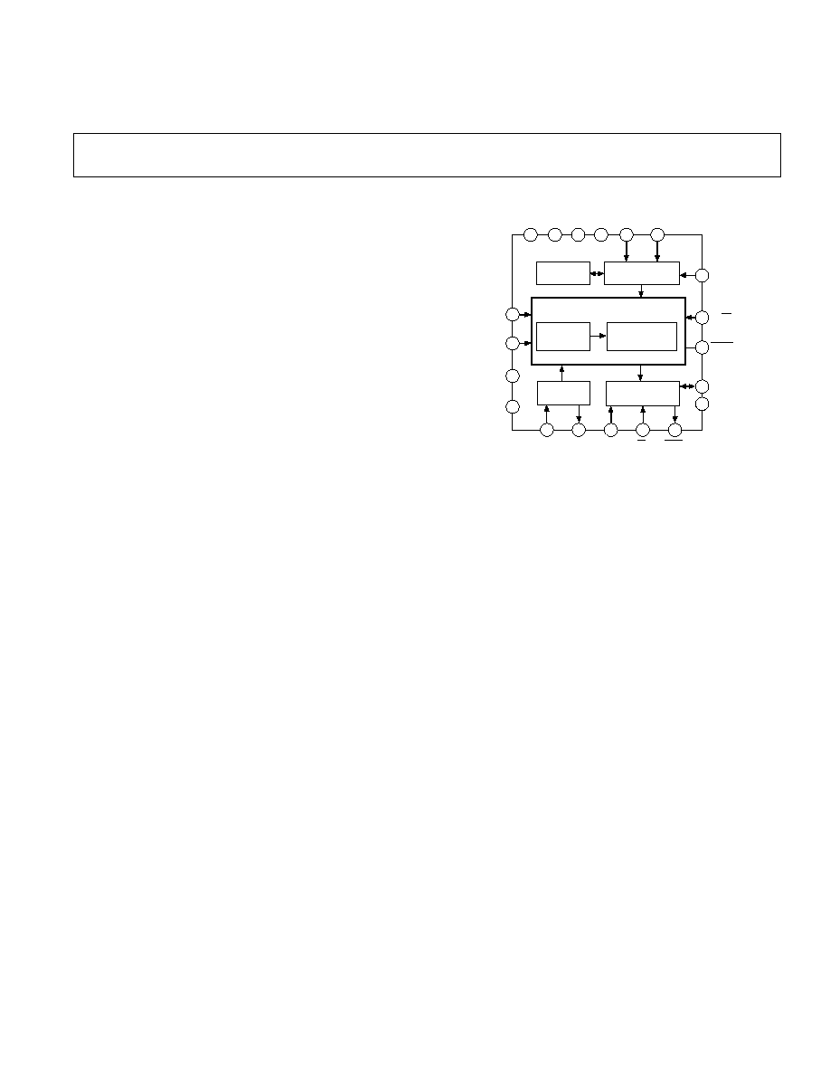
FUNCTIONAL BLOCK DIAGRAM
5
DGND
AV
DD
DV
DD
AV
SS
DV
SS
SC1
SC2
14
15
7
6
4
17
AGND
A
IN
V
REF
9
10
8
13
CALIBRATION
SRAM
CALIBRATION
MICROCONTROLLER
16-BIT A/D CONVERTER
ANALOG
MODULATOR
CAL
BP/UP
SLEEP
12
11
20
19
CLOCK
GENERATOR
SERIAL INTERFACE
LOGIC
SDATA
SCLK
3
2
1
16
18
CLKIN
CLKOUT
MODE
CS
DRDY
6-POLE GAUSSIAN
LOW-PASS
DIGITAL FILTER
AD7701

REV. D
2
(T
A
= +25 C; AV
DD
= DV
DD
= +5 V; AV
SS
= DV
SS
= 5 V; V
REF
= +2.5 V; f
CLKIN
=
4.096 MHz; Bipolar Mode: MODE = +5 V; A
IN
Source Resistance = 1k
1
with 1 nF to
AGND at A
IN
, unless otherwise noted.)
AD7701SPECIFICATIONS
Parameter
A, S Versions
2
B, T Versions
2
Units
Test Conditions/Comments
STATIC PERFORMANCE
Resolution
16
16
Bits
Integral Nonlinearity
T
MIN
to T
MAX
±
0.0007
% FSR typ
±
0.003
±
0.0015
% FSR max
Differential Nonlinearity
T
MIN
to T
MAX
±
0.125
±
0.125
LSB typ
Guaranteed No Missing Codes
±
0.5
±
0.5
LSB max
Positive Full-Scale Error
3
±
0.13
±
0.13
LSB typ
±
0.5
±
0.5
LSB max
Full-Scale Drift
4
±
1.2 (
±
2.3 S Version)
±
1.2 (
±
2.3 T Version)
LSB typ
Unipolar Offset Error
3
±
0.25
±
0.25
LSB typ
±
1
±
1
LSB max
Unipolar Offset Drift
4
±
1.6 (+3/25 S Version)
±
1.6 (+3/25 T Version)
LSB typ
Bipolar Zero Error
3
±
0.25
±
0.25
LSB typ
±
1
±
1
LSB max
Bipolar Zero Drift
4
±
0.8 (+1.5/12.5 S Version)
±
0.8 (+1.5/12.5 T Version)
LSB typ
Bipolar Negative Full-Scale Error
3
±
0.5
±
0.5
LSB typ
±
2
±
2
LSB max
Bipolar Negative Full-Scale Drift
4
±
0.6 (
±
1.2 S Version)
±
0.6 (
±
1.2 T Version)
LSB typ
Noise (Referred to Output)
0.1
0.1
LSB rms typ
DYNAMIC PERFORMANCE
Sampling Frequency, f
S
f
CLKIN
/256
f
CLKIN
/256
Hz
Output Update Rate, f
OUT
f
CLKIN
/1024
f
CLKIN
/1024
Hz
Filter Corner Frequency, f
3 dB
f
CLKIN
/409,600
f
CLKIN
/409,600
Hz
Settling Time to
±
0.0007% FS
507904/f
CLKIN
507904/f
CLKIN
sec
For Full-Scale Input Step
SYSTEM CALIBRATION
Applies to Unipolar and
Positive Full-Scale Overrange
V
REF
+ 0.1
V
REF
+ 0.1
V max
Bipolar Ranges. After Cali-
Positive Full-Scale Overrange
V
REF
+ 0.1
V
REF
+ 0.1
V max
bration, If A
IN
> V
REF
, the
Negative Full-Scale Overrange
(V
REF
+ 0.1)
(V
REF
+ 0.1)
V max
Device Will Output All 1s
Maximum Offset Calibration Range
5, 6
If A
IN
< 0 (Unipolar) or
Unipolar Input Range
(V
REF
+ 0.1)
(V
REF
+ 0.1)
V max
V
REF
(Bipolar), the Device
Bipolar Input Range
0.4 V
REF
to +0.4 V
REF
0.4 V
REF
to +0.4 V
REF
V max
Will Output All 0s.
Input Span
7
0.8 V
REF
0.8 V
REF
V min
2 V
REF
+ 0.2
2 V
REF
+ 0.2
V max
ANALOG INPUT
Unipolar Input Range
0 to +2.5
0 to +2.5
Volts
Bipolar Input Range
±
2.5
±
2.5
Volts
Input Capacitance
10
10
pF typ
Input Bias Current
1
1
1
nA typ
LOGIC INPUTS
All Inputs Except CLKIN
V
INL
, Input Low Voltage
0.8
0.8
V max
V
INH
, Input High Voltage
2.0
2.0
V min
CLKIN
V
INL
, Input Low Voltage
0.8
0.8
V max
V
INH
, Input High Voltage
3.5
3.5
V min
I
IN
, Input Current
10
10
µ
A max
LOGIC OUTPUTS
V
OL
, Output Low Voltage
0.4
0.4
V max
I
SINK
= 1.6 mA
V
OH
, Output High Voltage
DV
DD
1
DV
DD
1
V min
I
SOURCE
= 100
µ
A
Floating State Leakage Current
±
10
±
10
µ
A max
Floating State Output Capacitance
9
9
pF typ

Parameter
A, S Versions
2
B, T Versions
2
Units
Test Conditions/Comments
POWER REQUIREMENTS
8
Power Supply Voltages
Analog Positive Supply (AV
DD
)
4.5/5.5
4.5/5.5
V min/V max
Digital Positive Supply (DV
DD
)
4.5/AV
DD
4.5/AV
DD
V min/V max
Analog Negative Supply (AV
SS
)
4.5/5.5
4.5/5.5
V min/V max
Digital Negative Supply (DV
SS
)
4.5/5.5
4.5/5.5
V min/V max
Calibration Memory Retention
Power Supply Voltage
2.0
2.0
V min
DC Power Supply Currents
8
Analog Positive Supply (AI
DD
)
3.2
3.2
mA max
Typically 2 mA
Digital Positive Supply (DI
DD
)
1.5
1.5
mA max
Typically 1 mA
Analog Negative Supply (AI
SS
)
3.2
3.2
mA max
Typically 2 mA
Digital Negative Supply (DI
SS
)
0.1
0.1
mA max
Typically 0.03 mA
Power Supply Rejection
9
Positive Supplies
70
70
dB typ
Negative Supplies
75
75
dB typ
Power Dissipation
Normal Operation
40
40
mW max
SLEEP
= Logic 1,
Typically 25 mW
Standby Operation
10
20 (40 S Version)
20 (40 T Version)
µ
W max
SLEEP
= Logic 0,
Typically 10
µ
W
NOTES
1
1
The A
IN
pin presents a very high impedance dynamic load which varies with clock frequency.
1
2
Temperature ranges are as follows: A, B Versions; 40
°
C to +85
°
C; S, T Versions; 55
°
C to +125
°
C.
1
3
Apply after calibration at the temperature of interest. Full-scale error applies for both unipolar and bipolar input ranges.
1
4
Total drift over the specified temperature range since calibration at power-up at +25
°
C. This is guaranteed by design and/or characterization. Recalibration at any
temperature will remove these errors.
1
5
In unipolar mode the offset can have a negative value (V
REF
) such that the unipolar mode can mimic bipolar mode operation.
1
6
The specifications for input overrange and for input span apply additional constraints on the offset calibration range.
1
7
For unipolar mode, input span is the difference between full scale and zero scale. For bipolar mode, input span is the difference between positive and negative
full-scale points. When using less than the maximum input span, the span range may be placed anywhere within the range of
±
(V
REF
+0.1)
1
8
All digital outputs unloaded. All digital inputs at 5 V CMOS levels.
1
9
Applies in 0.1 Hz to 10 Hz bandwidth. PSRR at 60 Hz will exceed 120 dB due to the digital filter.
10
CLKIN is stopped. All digital inputs are grounded.
Specifications subject to change without notice.
REV. D
3
AD7701
WARNING!
ESD SENSITIVE DEVICE
CAUTION
ESD (electrostatic discharge) sensitive device. Electrostatic charges as high as 4000 V readily
accumulate on the human body and test equipment and can discharge without detection.
Although this device features proprietary ESD protection circuitry, permanent damage may
occur on devices subjected to high energy electrostatic discharges. Therefore, proper ESD
precautions are recommended to avoid performance degradation or loss of functionality.
ABSOLUTE MAXIMUM RATINGS
1
(T
A
= +25
°
C unless otherwise noted)
DV
DD
to AGND . . . . . . . . . . . . . . . . . . . . . . . 0.3 V to +6 V
DV
DD
to AV
DD
. . . . . . . . . . . . . . . . . . . . . . 0.3 V to +0.3 V
DV
SS
to AGND . . . . . . . . . . . . . . . . . . . . . . . . +0.3 V to 6 V
AV
DD
to AGND . . . . . . . . . . . . . . . . . . . . . . . . 0.3 V to +6 V
AV
SS
to AGND . . . . . . . . . . . . . . . . . . . . . . . . +0.3 V to 6 V
AGND to DGND . . . . . . . . . . . . . . . . . . . . 0.3 V to +0.3 V
Digital Input Voltage to DGND . . . . 0.3 V to DV
DD
+0.3 V
Analog Input
Voltage to AGND . . . . . . . . AV
SS
0.3 V to AV
DD
+ 0.3 V
Input Current to Any Pin Except Supplies
2
. . . . . . . .
±
10 mA
Operating Temperature Range
Commercial Plastic (A, B Versions) . . . . . 40
°
C to +85
°
C
Industrial Cerdip (A, B Versions) . . . . . . . 40
°
C to +85
°
C
Extended Cerdip (S, T Versions) . . . . . . 55
°
C to +125
°
C
Storage Temperature Range . . . . . . . . . . . 65
°
C to +150
°
C
Lead Temperature (Soldering, 10 secs) . . . . . . . . . . . +300
°
C
Power Dissipation (Any Package) to +75
°
C . . . . . . . 450 mW
Derates above +75
°
C by . . . . . . . . . . . . . . . . . . . . 10 mW/
°
C
NOTES
1
Stresses above those listed under "Absolute Maximum Ratings" may cause
permanent damage to the device. This is a stress rating only and functional
operation of the device at these or any other conditions above those listed in the
operational sections of this specification is not implied. Exposure to absolute
maximum rating conditions for extended periods may affect device reliability.
2
Transient currents of up to 100 mA will not cause SCR latch-up.
AD7701
REV. D
4
ORDERING GUIDE
Temperature
Linearity
Package
Model
Range
Error (% FSR) Options*
AD7701AN
40
°
C to +85
°
C
0.003
N-20
AD7701BN
40
°
C to +85
°
C
0.0015
N-20
AD7701AR
40
°
C to +85
°
C
0.003
R-20
AD7701BR
40
°
C to +85
°
C
0.0015
R-20
AD7701ARS
40
°
C to +85
°
C
0.003
RS-28
AD7701AQ
40
°
C to +85
°
C
0.003
Q-20
AD7701BQ
40
°
C to +85
°
C
0.0015
Q-20
AD7701SQ
55
°
C to +125
°
C
0.003
Q-20
AD7701TQ
55
°
C to +125
°
C
0.0015
Q-20
NOTES
*N = Plastic DIP; Q = Cerdip; R = SOIC; RS = SSOP.
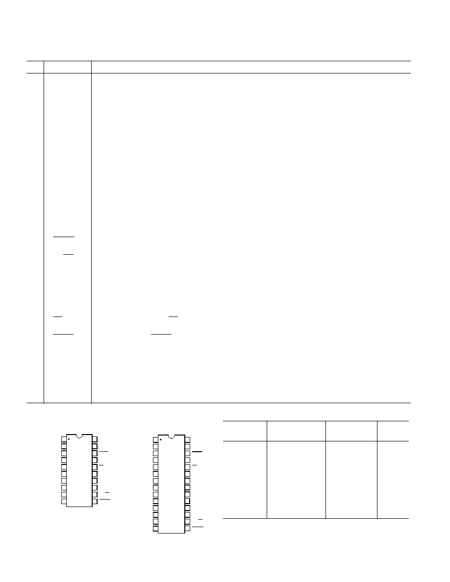
PIN FUNCTION DESCRIPTION
Pin
Mnemonic
Description
1
MODE
Selects the Serial Interface Mode. If MODE is tied to 5 V, the AD7701 will operate in the asynchronous
communications (ac) mode. The SCLK pin is configured as an input, and data is transmitted in two bytes,
each with one start bit and two stop bits. If MODE is tied to DGND, the synchronous external clocking
(SEC) mode is selected. SCLK is configured as an input, and the output appears without formatting, the
MSB coming first. If MODE is tied to +5 V, the AD7701 operates in the synchronous self-clocking (SSC)
mode. SCLK is configured as an output, with a clock frequency of f
CLKlN
/4 and 25% duty-cycle.
2
CLKOUT
Clock Output to generate an Internal Master Clock by connecting a crystal between CLKOUT and CLKIN.
If an external clock is used, CLKOUT is not connected.
3
CLKIN
Clock Input for External Clock.
4, 17
SC1, SC2
System Calibration Pins. The state of these pins, when CAL is taken high, determines the type of calibration
performed.
5
DGND
Digital Ground. Ground reference for all digital signals.
6
DV
SS
Digital Negative Supply, 5 V nominal.
7
AV
SS
Analog Negative Supply, 5 V nominal.
8
AGND
Analog Ground. Ground reference for all analog signals.
9
A
IN
Analog Input.
10
V
REF
Voltage Reference Input, +2.5 V nominal. This determines the value of positive full-scale in the unipolar
mode and of both positive and negative full-scale in the bipolar mode.
11
SLEEP
Sleep mode pin. When this pin is taken low, the AD7701 goes into a low-power mode with typically 10
µ
W
power consumption.
12
BP/UP
Bipolar/Unipolar Mode Pin. When this pin is low, the AD7701 is configured for a unipolar input range going
from AGND to V
REF
. When Pin 12 is high, the AD7701 is configured for a bipolar input range,
±
V
REF
.
13
CAL
Calibration Mode Pin. When CAL is taken high for more than 4 cycles, the AD7701 is reset and performs a
calibration cycle when CAL is brought low again. The CAL pin can also be used as a strobe to synchronize
the operation of several AD7701s.
14
AV
DD
Analog Positive Supply, +5 V nominal.
15
DV
DD
Digital Positive Supply, +5 V nominal.
16
CS
Chip Select Input. When CS is brought low, the AD7701 will begin to transmit serial data in a format deter-
mined by the state of the MODE pin.
18
DRDY
Data Ready output. DRDY is low when valid data is available in the output register. It goes high after transmission
of a word is completed. It also goes high for four clock cycles when a new data word is being loaded into the out-
put register, to indicate that valid data is not available, irrespective of whether data transmission is complete or not.
19
SCLK
Serial Clock Input/Output. The SCLK pin in configured as an input or output, dependent on the type of se-
rial data transmission that has been selected by the MODE pin. When configured as an output in the syn-
chronous self-clocking mode, it has a frequency of f
CLKIN
/4 and a duty cycle of 25%.
20
SDATA
Serial Data Output. The AD7701's output data is available at this pin as a 16-bit serial word. The transmis-
sion format is determined by the state of the MODE pin.
DIP, Cerdip, SOIC
MODE
SC1
DGND
CLKOUT
CLKIN
AGND
DV
SS
AV
SS
A
IN
V
REF
SDATA
SCLK
SC2
CAL
AV
DD
DV
DD
DRDY
CS
BP/UP
SLEEP
TOP VIEW
(Not to Scale)
AD7701
1
2
3
4
5
6
7
8
9
10
14
13
12
11
20
19
18
17
16
15
SSOP
MODE
SC1
DGND
CLKOUT
CLKIN
AGND
DV
SS
AV
SS
A
IN
V
REF
SDATA
SCLK
SC2
CAL
AV
DD
DV
DD
DRDY
CS
BP/UP
SLEEP
TOP VIEW
(Not to Scale)
AD7701
1
2
3
4
5
6
7
8
9
10
14
13
12
11
20
19
18
17
16
15
21
22
23
24
25
26
27
28
NC
NC
NC
NC
NC
NC
NC
NC
NC = NO CONNECT
PIN CONFIGURATIONS
5
REV. D
AD7701
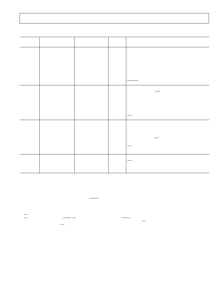
TIMING CHARACTERISTICS
1, 2
Limit at T
MIN
, T
MAX
Limit at T
MIN
, T
MAX
Parameter
(A, B Versions)
(S, T Versions)
Units
Conditions/Comments
f
CLKIN
3, 4
200
200
kHz min
Master Clock Frequency: Internal Gate Oscillator
5
5
MHz max Typically 4.096 MHz
200
200
kHz min
Master Clock Frequency: Externally Supplied
5
5
MHz max
t
r
5
50
50
ns max
Digital Output Rise Time. Typically 20 ns
t
f
5
50
50
ns max
Digital Output Fall Time. Typically 20 ns
t
1
0
0
ns min
SC1, SC2 to CAL High Setup Time
t
2
50
50
ns min
SC1, SC2 Hold Time After CAL Goes High
t
3
6
1000
1000
ns min
SLEEP
High to CLKIN High Setup Time
SSC Mode
t
4
7
3/f
CLKIN
3/f
CLKIN
ns max
Data Access Time (CS Low to Data Valid)
t
5
100
100
ns max
SCLK Falling Edge to Data Valid Delay (25 ns typ)
t
6
250
250
ns min
MSB Data Setup Time. Typically 380 ns
t
7
300
300
ns max
SCLK High Pulse Width. Typically 240 ns
t
8
790
790
ns max
SCLK Low Pulse Width. Typically 730 ns
t
9
8
l/f
CLKIN
+200
l/f
CLKIN
+200
ns max
SCLK Rising Edge to Hi-Z Delay (l/f
CLKIN
+ 100 ns typ)
t
10
8, 9
(4/f
CLKIN
) +200
(4/f
CLKIN
) +200
ns max
CS
High to Hi-Z Delay
SEC Mode
f
SCLK
5
5
MHz
Serial Clock Input Frequency
t
11
35
35
ns min
SCLK Input High Pulse Width
t
12
160
160
ns min
SCLK Low Pulse Width
t
13
7, 10
160
160
ns max
Data Access Time (CS Low to Data Valid). Typically 80 ns
t
14
11
150
150
ns max
SCLK Falling Edge to Data Valid Delay. Typically 75 ns
t
15
8
250
250
ns max
CS
High to Hi-Z Delay
t
16
8
200
200
ns max
SCLK Falling Edge to Hi-Z Delay. Typically 100 ns
AC Mode
t
17
40
40
ns min
CS
Setup Time. Typically 20 ns
t
18
180
180
ns max
Data Delay Time. Typically 90 ns
t
19
200
200
ns max
SCLK Falling Edge to Hi-Z Delay. Typically 100 ns
NOTES
1
1
Sample tested at +25
°
C to ensure compliance. All input signals are specified with t
r
= t
f
= 5 ns (10% to 90% of 5 V) and timed from a voltage level of 1.6 V.
1
2
See Figures 1 to 6.
1
3
CLKIN Duty Cycle range is 20% to 80%. CLKIN must be supplied whenever the AD7701 is not in SLEEP mode. If no clock is present in this case, the device can
draw higher current than specified and possibly become uncalibrated.
1
4
The AD7701 is production tested with f
CLKIN
at 4.096 MHz. It is guaranteed by characterization to operate at 200 kHz.
1
5
Specified using 10% and 90% points on waveform of interest.
1
6
In order to synchronize several AD7701s together using the SLEEP pin, this specification is met.
1
7
t
4
and t
13
are measured with the load circuit of Figure 1 and defined as the time required for an output to cross 0.8 V or 2.4 V.
1
8
t
9
, t
10
, t
15
and t
16
are derived from the measured time taken by the data outputs to change 0.5 V when loaded with the circuit of Figure 1. The measured number is
then extrapolated back to remove the effects of charging or discharging the 100 pF capacitor. This means that the time quoted in the Timing Characteristics is the
true bus relinquish time of the part and as such as independent of external bus loading capacitance.
1
9
If CS is returned high before all 16 bits are output, the SDATA and SCLK outputs will complete the current data bit and then go to high impedance.
10
If CS is activated asynchronously to DRDY, CS will not be recognized if it occurs when DRDY is high for four clock cycles. The propagation delay time may be as
great as 4 CLKIN cycles plus 160 ns. To guarantee proper clocking of SDATA when using asynchronous CS, the SCLK input should not be taken high sooner than
4 CLKIN cycles plus 160 ns after CS goes low.
11
SDATA is clocked out on the falling edge of the SCLK input.
(AV
DD
= DV
DD
= +5 V 10%; AV
SS
= DV
SS
= 5 V 10%; AGND = DGND = O V;
f
CLKIN
= 4.096 MHz; Input Levels: Logic O = O V, Logic 1 = DV
DD
)
AD7701
REV. D
6
1.6mA
200
µ
A
C
L
100pF
TO
OUTPUT
PIN
IOH
2.1V
+
I
OL
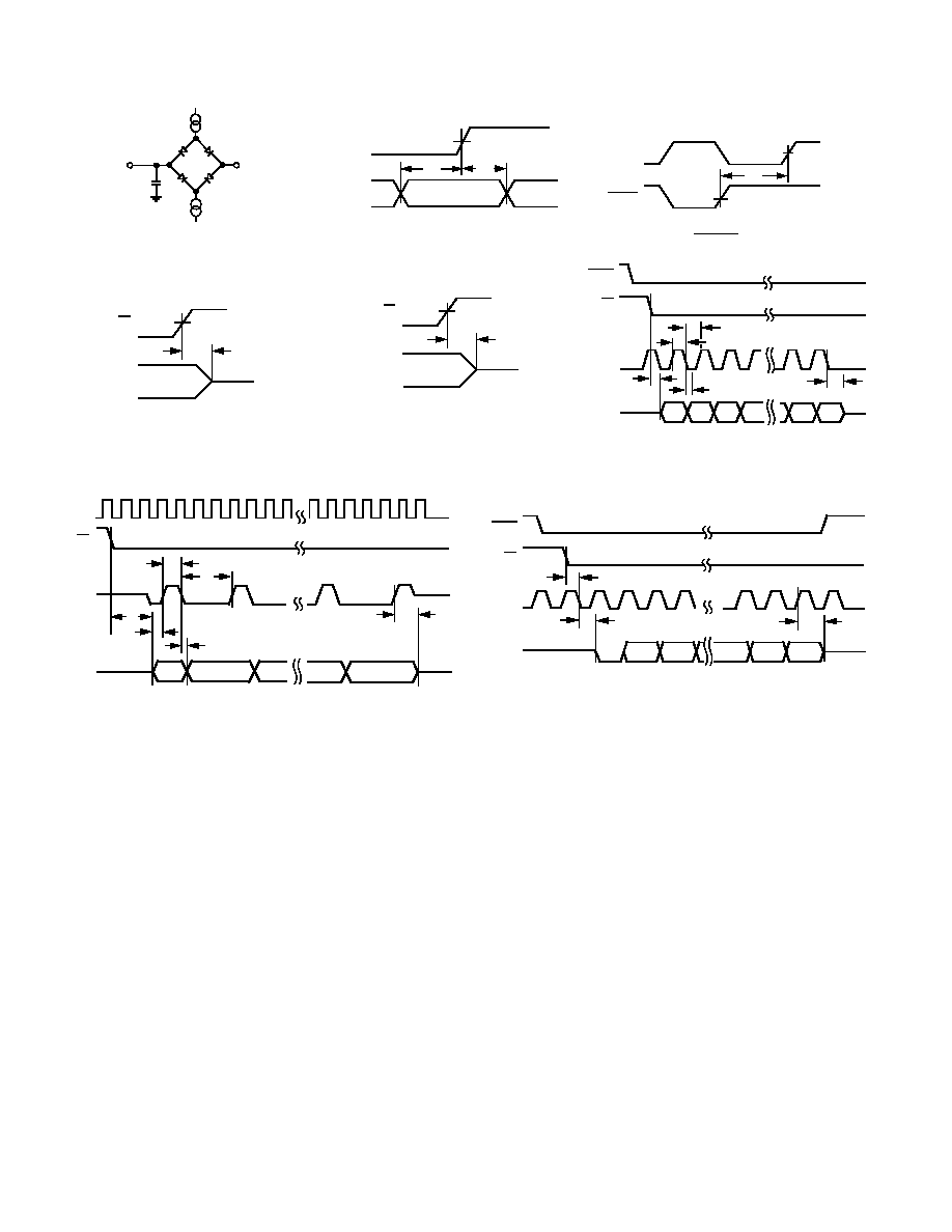
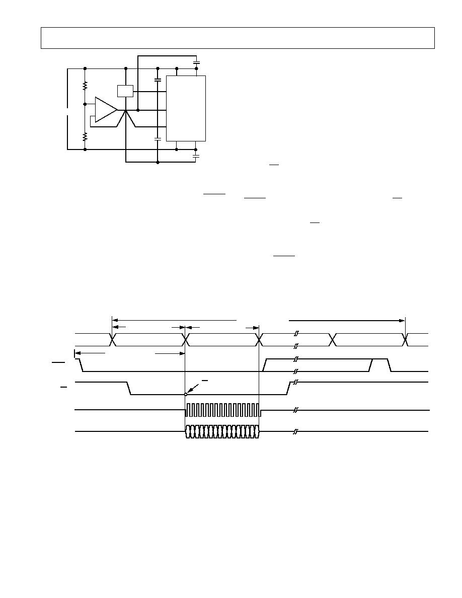
Figure 1. Load Circuit for Access
Time and Bus Relinquish Time
DATA
VALID
t
10
HI-Z
SDATA
CS
Figure 3. SSC Mode Data Hold
Time
CAL
SC1, SC2
SC1,SC2 VALID
t
1
t
2
Figure 2a. Calibration Control Timing
DATA
VALID
t
15
HI-Z
SDATA
CS
Figure 4a. SEC Mode Data Hold Time
CLKIN
SLEEP
t
3
Figure 2b. SLEEP Mode Timing
HI-Z
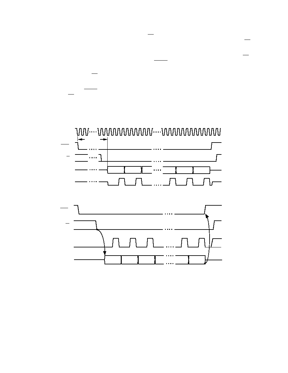
DB15
DB14
DB1
DB0
HI-Z
SDATA
DRDY
CS
t
12
t
11
t
13
t
14
SCLK
t
16
Figure 4b. SEC Mode Timing Diagram
TERMINOLOGY
LINEARITY ERROR
This is the maximum deviation of any code from a straight line
passing through the endpoints of the transfer function. The
endpoints of the transfer function are Zero-Scale (not to be
confused with Bipolar Zero), a point 0.5 LSB below the first
code transition (000 . . . 000 to 000 . . . 001) and Full-Scale, a
point 1.5 LSB above the last code transition (111 . . . 110 to
111 . . . 111). The error is expressed as a percentage of full
scale.
DIFFERENTIAL LINEARITY ERROR
This is the difference between any code's actual width and the
ideal (1 LSB) width. Differential Linearity Error is expressed in
LSBs. A differential linearity specification of
±
1 LSB or less
guarantees monotonicity.
POSITIVE FULL-SCALE ERROR
Positive Full-Scale Error is the deviation of the last code
transition (111 . . . 110 to 111 . . . 111) from the ideal (V
REF
3/2 LSBs). It applies to both positive and negative analog input
ranges and it is expressed in microvolts.
UNIPOLAR OFFSET ERROR
Unipolar Offset Error is the deviation of the first code transition
from the ideal (AGND + 0.5 LSB) when operating in the uni-
polar mode. It is expressed in microvolts.
BIPOLAR ZERO ERROR
This is the deviation of the midscale transition (0111 . . . 111 to
1000 . . . 000) from the ideal (AGND 0.5 LSB) when
operating in the bipolar mode. It is expressed in microvolts.
BIPOLAR NEGATIVE FULL-SCALE ERROR
This is the deviation of the first code transition from the ideal
(V
REF
+ 0.5 LSB), when operating in the bipolar mode. It is
expressed in microvolts.
POSITIVE FULL-SCALE OVERRANGE
Positive Full-Scale Overrange is the amount of overhead avail-
able to handle input voltages greater than +V
REF
( for example,
noise peaks or excess voltages due to system gain errors in
system calibration routines) without introducing errors due to
overloading the analog modulator or overflowing the digital
filter. It is expressed in millivolts.
NEGATIVE FULL-SCALE OVERRANGE
This is the amount of overhead available to handle voltages
below V
REF
without overloading the analog modulator or
overflowing the digital filter. Note that the analog input will
accept negative voltage peaks even in the unipolar mode. The
overhead is expressed in millivolts.
HI-Z
DB15
DB14
DB1
DB0
HI-Z
SCLK
SDATA
CLKIN
CS
HI-Z
t
7
t
6
t
5
t
9
t
4
t
8
Figure 5. SSC Mode Timing Diagram
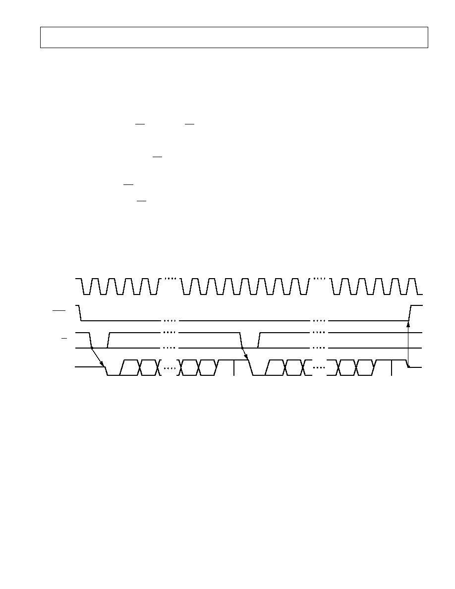
HI-Z
START
DB8
DB9
DB7
STOP 1
STOP 2
HI-Z
HIGH BYTE
LOW BYTE
SDATA
SCLK
DRDY
CS
t
17
t
18
t
19
Figure 6. AC Mode Timing Diagram
7
REV. D
AD7701
The AD7701 can perform self-calibration using the on-chip
calibration microcontroller and SRAM to store calibration
parameters. A calibration cycle may be initiated at any time
using the CAL control input.
Other system components may also be included in the
calibration loop to remove offset and gain errors in the input
channel.
For battery operation, the AD7701 also offers a standby mode
that reduces idle power consumption to typically 10
µ
W.
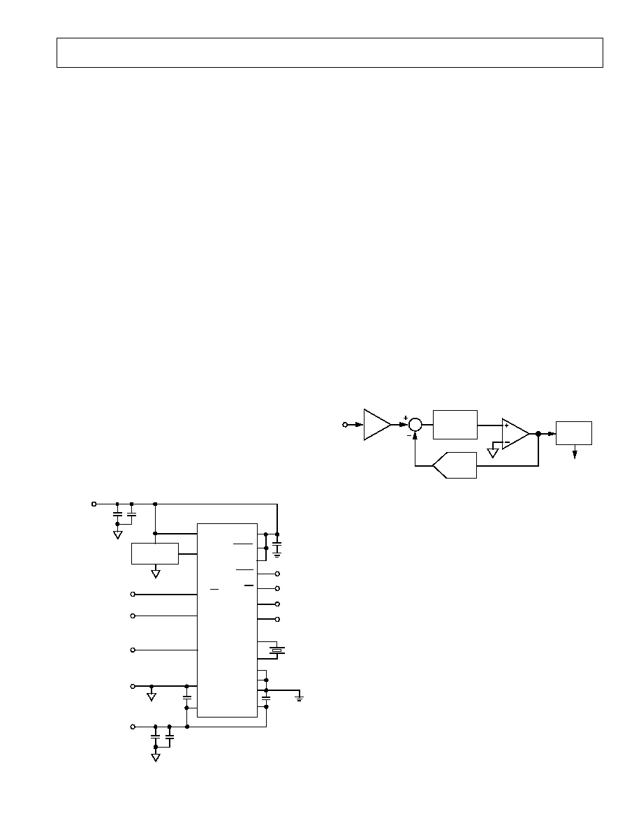
THEORY OF OPERATION
The general block diagram of a sigma-delta ADC is shown in
Figure 8. It contains the following elements.
1. A sample-hold amplifier.
2. A differential amplifier or subtracter.
3. An analog low-pass filter.
4. A 1-bit A/D converter (comparator).
5. A 1-bit DAC.
6. A digital low-pass filter.
In operation, the analog signal sample is fed to the subtracter,
along with the output of the 1-bit DAC. The filtered difference
signal is fed to the comparator, whose output samples the
difference signal at a frequency many times that of the analog
signal sampling frequency (oversampling).
ANALOG
LOW-PASS
FILTER
COMPARATOR
DIGITAL
FILTER
DIGITAL DATA
S/H AMP
DAC
Figure 8. General Sigma-Delta ADC
Oversampling is fundamental to the operation of sigma-delta
ADCs. Using the quantization noise formula for an ADC:
SNR = (6.02
×
number of bits + 1.76) dB
a 1-bit ADC or comparator yields an SNR of 7.78 dB.
The AD7701 samples the input signal at 16 kHz, which spreads
the quantization noise from 0 to 8 kHz. Since the specified
analog input bandwidth of the AD7701 is only 0 to 10 Hz, the
noise energy in this bandwidth would be only 1/800 of the total
quantization noise, even if the noise energy was spread evenly
throughout the spectrum. It is reduced still further by analog
filtering in the modulator loop, which shapes the quantization
noise spectrum to move most of the noise energy to frequencies
above 10 Hz. The SNR performance in the 0 to 10 Hz range is
conditioned to the 16-bit level in this fashion.
The output of the comparator provides the digital input for the
1-bit DAC, so that the system functions as a negative feedback
loop that tries to minimize the difference signal. The digital data
that represents the analog input voltage is contained in the duty
cycle of the pulse train appearing at the output of the compara-
tor. It can be retrieved as a parallel binary data word using a
digital filter.
OFFSET CALIBRATION RANGE
In the system calibration modes (SC2 low) the AD7701
calibrates its offset with respect to the A
IN
pin. The Offset
Calibration Range specification defines the range of voltages,
expressed as a percentage of V
REF
that the AD7701 can accept
and still calibrate offset accurately.
FULL-SCALE CALIBRATION RANGE
This is the range of voltages that the AD7701 can accept in the
system calibration mode and still calibrate full-scale correctly.
INPUT SPAN
In system calibration schemes, two voltages applied in sequence
to the AD7701's analog input define the analog input range.
The input span specification defines the minimum and maxi-
mum input voltages from zero to full-scale that the AD7701 can
accept and still calibrate gain accurately. The input span is ex-
pressed as a percentage of V
REF.
GENERAL DESCRIPTION
The AD7701 is a 16-bit A/D converter with on-chip digital
filtering, intended for the measurement of wide dynamic range,
low frequency signals such as those representing chemical,
physical or biological processes. It contains a charge-balancing
(sigma-delta) ADC, calibration microcontroller with on-chip
static RAM, a clock oscillator and a serial communications port.
The analog input signal to the AD7701 is continuously sampled
at a rate determined by the frequency of the master clock,
CLKIN. A charge-balancing A/D converter (Sigma-Delta
Modulator) converts the sampled signal into a digital pulse train
whose duty cycle contains the digital information. A six-pole
Gaussian digital low-pass filter processes the output of the
modulator and updates the 16-bit output register at a 4 kHz
rate. The output data can be read from the serial port randomly
or periodically at any rate up to 4 kHz.
AD7701
MODE
SDATA
SC1
DGND
CLKOUT
CLKIN
AGND
SCLK
SC2
CAL
CS
BP/UP
DV
SS
DV
DD
SLEEP
RANGE
SELECT
CALIBRATE
ANALOG
INPUT
ANALOG
GROUND
5V
ANALOG
SUPPLY
0.1
µ
F
SERIAL
DATA
SERIAL
CLOCK
READ
(TRANSMIT)
DATA
READY
+5V
ANALOG
SUPPLY
2.5V
0.1
µ
F
0.1
µ
F
VOLTAGE
REFERENCE
DRDY
0.1
µ
F
10
µ
F
AV
DD
V
REF
A
IN
AV
SS
0.1
µ
F
10
µ
F
Figure 7. Typical System Connection Diagram
AD7701
REV. D
8
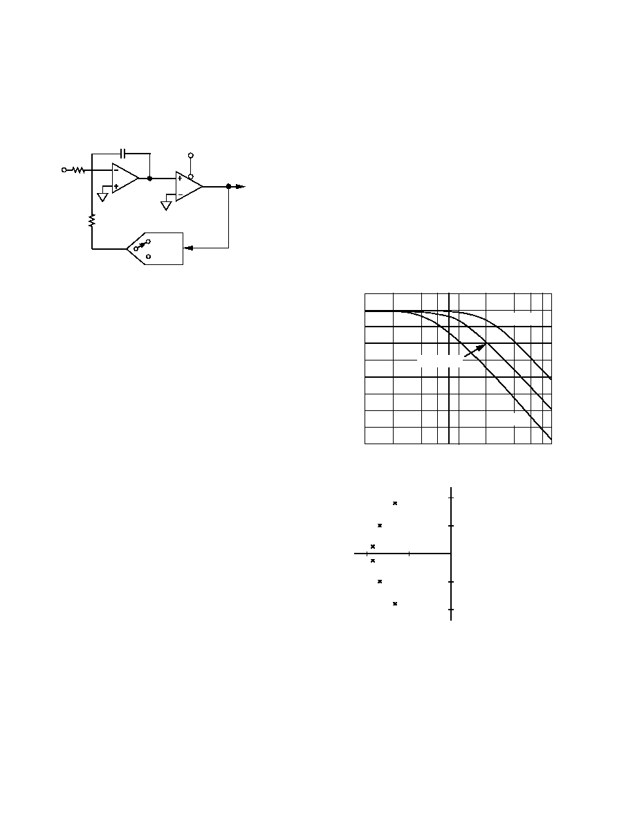
FILTER CHARACTERISTICS
The cutoff frequency of the digital filter is f
CLK
/409600. At the
maximum clock frequency of 4.096 MHz, the cutoff frequency
of the filter is 10 Hz and the output rate is 4 kHz.
Figure 10 shows the filter frequency response. This is a 6-pole
Gaussian response that provides 55 dB of 60 Hz rejection for a
10 Hz cutoff frequency. If the clock frequency is halved to give a
5 Hz cutoff, 60 Hz rejection is better than 90 dB. A normalized
s-domain pole-zero plot of the filter is shown in Figure 11.
The response of the filter is defined by:
H(x) = [1+ 0.693x
2
+ 0.240x
4
+ 0.0555x
6
+ 0.00962x
8
+ 0.00133x
10
+ 0.000154x
12
]
0.5
where:
x = f/f
3 dB
, f
3 dB
= f
CLKIN
/409600,
and
f is the frequency of interest.
f
CLK
= 2MHz
f
CLK
= 1MHz
f
CLK
= 4MHz
1
10
100
FREQUENCY Hz
20
0
20
40
60
80
100
120
140
160
GAIN dBs
Figure 10. Frequency Response of AD7701 Filter
jw
s
0
j1
j2
2
1
j1
j2
S1,2 = 1.4663 + j1.8191
S3,4 = 1.7553 + j1.0005
S5,6 = 1.8739 + j0.32272
Figure 11. Normalized Pole-Zero Plot of AD7701 Filter
Since the AD7701 contains this on-chip, low-pass filtering,
there is a settling time associated with step function inputs, and
data will be invalid after a step change until the settling time has
elapsed. The AD7701 is therefore unsuitable for high speed
multiplexing, where channels are switched and converted se-
quentially at high rates, as switching between channels can
cause a step change in the input. Rather, it is intended for dis-
tributed converter systems using one ADC per channel.
However, slow multiplexing of the AD7701 is possible, provided
that the settling time is allowed to elapse before data for the new
channel is accessed.
Sigma-delta ADCs are generally described by the order of the
analog low-pass filter. A simple example of a first order sigma-
delta ADC is shown in Figure 9. This contains only a first-order
low-pass filter or integrator. It also illustrates the derivation of
the alternative name for these devices: Charge-Balancing ADCs.
C
R
R
A
IN
INTEGRATOR
TO DIGITAL
FILTER
CLOCK
1-BIT DAC
STROBED
COMPARATOR
+V
REF
V
REF
Figure 9. SEC Basic Charge-Balancing ADC
The term charge-balancing comes from the fact that this system
is a negative feedback loop that tries to keep the net charge on
the integrator capacitor at zero, by balancing charge injected by
the input voltage with charge injected by the 1-bit DAC. When
the analog input is zero, the only contribution to the integrator
output comes from the 1-bit DAC. For the net charge on the
integrator capacitor to be zero, the DAC output must spend half
its time at +1 V and half its time at 1 V. Assuming ideal
components, the duty cycle of the comparator will be 50%.
When a positive analog input is applied, the output of the 1-bit
DAC must spend a larger proportion of the time at +1 V, so the
duty cycle of the comparator increases. When a negative input
voltage is applied, the duty cycle decreases.
The AD7701 uses a second-order sigma-delta modulator and a
sophisticated digital filter that provides a rolling average of the
sampled output. After power-up or if there is a step change in
the input voltage, there is a settling time that must elapse before
valid data is obtained.
DIGITAL FILTERING
The AD7701's digital filter behaves like a similar analog filter,
with a few minor differences.
First, since digital filtering occurs after the A to D conversion
process, it can remove noise injected during the conversion
process. Analog filtering cannot do this.
On the other hand, analog filtering can remove noise super-
imposed on the analog signal before it reaches the ADC. Digital
filtering cannot do this and noise peaks riding on signals near
full scale have the potential to saturate the analog modulator
and digital filter, even though the average value of the signal is
within limits. To alleviate this problem, the AD7701 has over-
range headroom built into the sigma-delta modulator and digital
filter which allows overrange excursions of 100 mV. If noise
signals are larger than this, consideration should be given to
analog input filtering, or to reducing the gain in the input
channel so that a full-scale input (2.5 V) gives only a half-scale
input to the AD7701 (1.25 V). This will provide an overrange
capability greater than 100% at the expense of reducing the
dynamic range by 1 bit (50%).
9
REV. D
AD7701
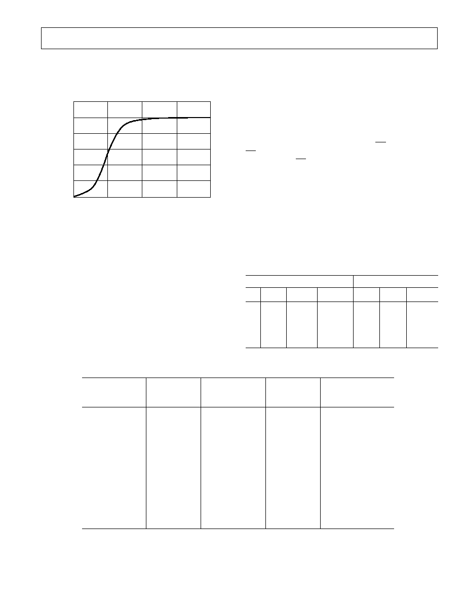
The output settling of the AD7701 in response to a step input
change is shown in Figure 12. The Gaussian response has fast
settling with no overshoot, and the worst-case settling time to
±
0.0007% (
±
0.5 LSB) is 125 ms with a 4.096 MHz master
clock frequency.
PERCENT OF FINAL VALUE
100
80
60
40
20
0
0
40
80
120
160
TIME ms
Figure 12. AD7701 Step Response
USING THE AD7701
SYSTEM DESIGN CONSIDERATIONS
The AD7701 operates differently from successive approxima-
tion ADCs or other integrating ADCs. Since it samples the sig-
nal continuously, like a tracking ADC, there is no need for a
start convert command. The 16-bit output register is updated at
a 4 kHz rate, and the output can be read at any time, either syn-
chronously or asynchronously.
CLOCKING
The AD7701 requires a master clock input, which may be an
external TTL/CMOS compatible clock signal applied to the
CLKIN pin (CLKOUT not used). Alternatively, a crystal of the
correct frequency can be connected between CLKIN and
CLKOUT, when the clock circuit will function as a crystal-
controlled oscillator.
The input sampling frequency, output data rate, filter character-
istics and calibration time are all directly related to the master
clock frequency f
CLKIN
by the ratios given in the specification
table. Therefore, the first step in system design with the
AD7701 is to select a master clock frequency suitable for the
bandwidth and output data rate required by the application.
ANALOG INPUT RANGES
The AD7701 performs conversion relative to an externally
supplied reference voltage, which allows easy interfacing to
ratiometric systems. In addition, either unipolar or bipolar input
voltage range may be selected using the BP/UP input. With BP/
UP
tied low, the input range is unipolar and the span is 0 to
+V
REF
. With BP/UP tied high, the input range is bipolar and the
span is
±
V
REF
. In the bipolar mode both positive and negative
full scale are directly determined by V
REF
. This offers superior
tracking of positive and negative full scale and better midscale
(bipolar zero) stability than bipolar schemes that simply scale
and offset the input range.
The digital output coding for the unipolar range is Unipolar
Binary; for the bipolar range it is Offset Binary. Bit weights for
the unipolar and bipolar modes are shown in Table I. The input
voltages and output codes for unipolar and bipolar ranges, using
the recommended +2.5 V reference, are shown in Table II.
Table I. Bit Weight Table (2.5 V Reference Voltage)
Unipolar Mode
Bipolar Mode
V
LSBs
% FS
ppm FS
LSBs % FS
ppm FS
10
0.26
0.0004
4
0.13
0.0002
2
19
0.5
0.0008
8
0.26
0.0004
4
38
1.00
0.0015
15
0.5
0.0008
8
76
2.00
0.0031
31
1.00
0.0015
15
153
4.00
0.0061
61
2.00
0.0031
31
Table II. Output Coding
Unipolar Mode
Bipolar Mode
Input Relative to
Input in Volts
Input Relative to
Input in Volts
Output Data
FS and AGND
FS and AGND
1111 1111 1111 1111
+V
REF
1.5 LSB
+2.499943
+V
REF
1.5 LSB
+2.499886
1111 1111 1111 1110
+V
REF
2.5 LSB
+2.499905
+V
REF
2.5 LSB
+2.499810
1111 1111 1111 1101
+V
REF
3.5 LSB
+2.499867
+V
REF
3.5 LSB
+2.499733
1111 1111 1111 1100
1000 0000 0000 0001
+V
REF
/2 + 0.5 LSB
+1.250019
AGND + 0.5 LSB
+0.000038
1000 0000 0000 0000
+V
REF
/2 0.5 LSB
+1.249981
AGND 0.5 LSB
0.000038
0111 1111 1111 1111
+V
REF
/2 1.5 LSB
+1.249943
AGND 1.5 LSB
0.000114
0111 1111 1111 1110
0000 0000 0000 0011
AGND + 2.5 LSB
+0.000095
V
REF
+ 2.5 LSB
2.499810
0000 0000 0000 0010
AGND + 1.5 LSB
+0.000057
V
REF
+ 1.5 LSB
2.499886
0000 0000 0000 0001
AGND + 0.5 LSB
+0.000019
V
REF
+ 0.5 LSB
2.499962
0000 0000 0000 0000
NOTES
1
V
REF
= +2.5 V
2
AGND = 0 V
3
Unipolar Mode, 1 LSB = 2.5 V/655536 = 0.000038 V
4
Bipolar Mode, 1 LSB = 5 V/65536 = 0.000076 V
5
Inputs are voltages at code transitions.
AD7701
REV. D
10
INPUT SIGNAL CONDITIONING
Reference voltages from +1 V to +3 V may be used with the
AD7701, with little degradation in performance. Input ranges
that cannot be accommodated by this range of reference voltages
may be achieved by input signal conditioning. This may take the
form of gain to accommodate a smaller signal range, or passive
attenuation to reduce a larger input voltage range.
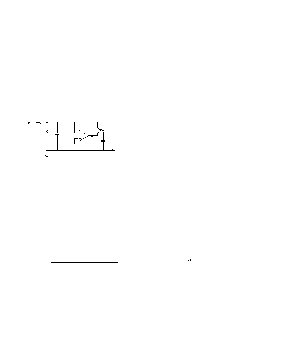
Source Resistance
If passive attenuators are used in front of the AD7701, care
must be taken to ensure that the source impedance is suffi-
ciently low. The AD7701 has an analog input with over 1 G
dc input resistance. In parallel with this there as a small dy-
namic load which varies with the clock frequency (see Figure
13). Each time the analog input is sampled, a 10 pF capacitor
draws a charge packet of maximum 1 pC (10 pF
×
100 mV)
A
IN
R1
R2
C
EXT
AGND
AD7701
V
OS
100mV
C
IN
10pF
Figure 13. Equivalent Input Circuit and Input Attenuator
from the analog source with a frequency f
CLKIN
/256. For a
4.096 MHz CLKIN, this yields an average current draw of
16 nA. After each sample the AD7701 allows 62 clock periods
for the input voltage to settle. The equation which defines
settling time is:
V
O
= V
IN
[1 e
t/RC
]
where:
V
O
is the final settled value,
V
IN
is the value of the input signal,
R
is the value of the input source resistance,
C
is the 10 pF sample capacitor,
t
is equal to 62/f
CLKIN
.
From this, the following equation can be developed which gives
the maximum allowable source resistance, R
S(MAX)
, for an error
of V
E
:
R
S (MAX )
=
62
f
CLKIN
×
(10 pF )
×
l n (100mV /V
E
)
Provided the source resistance is less than this value, the analog
input will settle within the desired error band in the requisite 62
clock periods. Insufficient settling leads to offset errors. These
can be calibrated in system calibration schemes.
If a limit of 10
µ
V (0.25 LSB at 16 bits) is set for the maximum
offset voltage, then the maximum allowable source resistance is
160 k
from the above equation, assuming that there is no
external stray capacitance.
An RC filter may be added in front of the AD7701 to reduce
high frequency noise. With an external capacitor added from
A
IN
to AGND, the following equation will specify the maximum
allowable source resistance:
R
S (Max)
=
62
f
CLKIN
×
(
C
IN
+
C
EXT
)
×
ln
100 mV
×
C
IN
/ (C
IN
+
C
EXT
)
V
E
The practical limit to the maximum value of source resistance is
thermal (Johnson) noise. A practical resistor may be modeled as
an ideal (noiseless) resistor in series with a noise voltage source
or in parallel with a noise current source.
V
n
=
4 kTRf
Volts
i
n
=
4 kTf / R
Amperes
where:
k is Boltzmann's constant (1.38
×
10
23
J/K)
and
T is temperature in degrees Kelvin (
°
C + 273).
Active signal conditioning circuits such as op amps generally do
not suffer from problems of high source impedance. Their open
loop output resistance is normally only tens of ohms and, in any
case, most modern general purpose op amps have sufficiently
fast closed loop settling time for this not to be a problem. Offset
voltage in op amps can be eliminated in a system calibration
routine. With the wide dynamic range and small LSB size of the
AD7701, noise can also be a problem, but the digital filter will
reject most broadband noise above its cutoff frequency. How-
ever, in certain applications there may be a need for analog
input filtering.
Antialias Considerations
The digital filter of the AD7701 does not provide any rejection
at integer multiples of the sampling frequency (nf
CLKlN
/256,
where n = 1, 2, 3 . . . ).
With a 4.096 MHz master clock there are narrow (
±
10 Hz)
bands at 16 kHz, 32 kHz, 48 kHz, etc., where noise passes
unattenuated to the output.
However, due to the AD7701's high oversampling ratio of 800
(16 kHz to 20 Hz) these bands occupy only a small fraction of
the spectrum, and most broadband noise is filtered. The
reduction in broadband noise is given by:
e
OUT
=
e
IN
2 f
C
/ f
S
=
0.035 e
IN
where:
e
lN
and e
OUT
are rms noise terms referred to the input
f
C
is the filter 3 dB corner frequency
(f
CLKIN
/409600)
and
f
S
is the sampling frequency (f
CLKIN
/256).
Since the ratio of f
S
to f
CLKIN
is fixed, the digital filter reduces
broadband white noise by 96.5% independent of the master
clock frequency.

11
REV. D
AD7701
VOLTAGE REFERENCE CONNECTIONS
The voltage applied to the V
REF
pin defines the analog input
range. The specified reference voltage is 2.5 V, but the AD7701
will operate with reference voltages from 1 V to 3 V with little
degradation in performance.
The reference input presents exactly the same dynamic load as
the analog input, but in the case of the reference input, source
resistance and long settling time introduce gain errors rather
than offset errors. Fortunately, most precision references have
sufficiently low output impedance and wide enough bandwidth
to settle to 10
µ
V within 62 clock cycles.
AGND
AD7701
+5V
AV
DD
V
REF
LT1019
Figure 14. Typical External Reference Connections
The digital filter of the AD7701 removes noise from the
reference input, just as it does with noise at the analog input,
and the same limitations apply regarding lack of noise rejection
at integer multiples of the sampling frequency. If reference noise
is a problem, some voltage references offer noise reduction
schemes using an external capacitor. Alternatively, a simple RC
filter may be used, as shown in Figure 15.
+5V
AD580
AGND
AD7701
AV
DD
V
REF
R
F
13k
C
F
100pF
Figure 15. Filtered Reference Input
The same considerations apply to this filter as to a filter at the
analog input. In this case:
[R
F
(C
F
+
10 pF )]
=
62
f
CLKIN
×
ln
100 mV
×
C
IN
(C
IN
+
C
F
)
V
FSE
where:
f
CLKIN
is the master clock frequency
and
V
FSE
is the maximum desired error in volts.
GROUNDING AND SUPPLY DECOUPLING
AGND is the ground reference voltage for the AD7701, and is
completely independent of DGND. Any noise riding on the
AGND input with respect to the system analog ground will
cause conversion errors. AGND should therefore be used as the
system ground and also as the ground for the analog input and
the reference voltage.
The analog and digital power supplies to the AD7701 are
independent and separately pinned out, to minimize coupling
between analog and digital sections of the device. The digital
filter will provide rejections of broadband noise on the power
supplies, except at integer multiples of the sampling frequency.
Therefore, the two analog supplies should be decoupled to
AGND using 100 nF ceramic capacitors to provide power
supply noise rejections at these frequencies. The two digital
supplies should similarly be decoupled to DGND.
ACCURACY AND AUTOCALIBRATION
Sigma-delta ADCs, like VFCs and other integrating ADCs, do
not contain any source of nonmonotonicity and inherently offer
no-missing-codes performance. The AD7701 achieves excellent
linearity (
±
0.0007%) by the use of high quality, on-chip silicon
dioxide capacitors, which have a very low capacitance/voltage
coefficient.
The AD7701 offers two self-calibration modes using the on-chip
calibration microcontroller and SRAM. Table III is a truth table
for the calibration control inputs SC1 and SC2.
In the self-calibration mode, zero-scale is calibrated against the
AGND pin and full scale is calibrated against the V
REF
pin, to
remove internal errors.
Note that in the bipolar mode the AD7701 calibrates positive
full scale and midscale (bipolar zero).
In the system-calibration mode, the AD7701 calibrates its zero
and full scale to voltages present on the analog input pin in two
sequential steps. This allows system offsets and/or gain errors to
be nulled out.
SYSTEM
REF HI
A
IN
SYSTEM
REF LO
ANALOG
MUX
A0
A1
SIGNAL
CONDITIONING
AD7701
MICRO
COMPUTER
SCLK
SDATA
CAL
SC1
SC2
Figure 16. Typical Connections for System Calibration
A typical system calibration scheme is shown in Figure 16. In
normal operation the analog signal is fed to the AD7701 via an
analog multiplexer. When the system is to be calibrated, A
IN
is
first switched to the system REF LO via the multiplexer and
CAL is strobed high, with SC1 and SC2 both high. AIN is then
switched to the system REF HI and CAL is strobed, with SC1
low and SC2 high. In this way, the effect of all error sources

AD7701
REV. D
12
between the multiplexer and the AD7701 is removed. Op amps
and other signal conditioning circuits may be used in front of
the AD7701, without worrying about their absolute gain or
offset errors. Note that the absolute value of the reference
supplied to the AD7701 is no longer important, provided it has
adequate short-term stability between calibration cycles, as full
scale is calibrated to the system reference.
If system offset errors are important but system gain errors are
not, then a one step system calibration may be performed with
SC1 high and SC2 low. In this case, offset is calibrated against
A
IN
, which should be connected to system REF LO during
calibration, but full scale is calibrated against the AD7701's
V
REF
input.
System calibration schemes will yield better accuracy than self-
calibration, even if there are no system errors. Using self-
calibration, errors arise due to the mismatch in source impedances
between the references during calibration (AGND and V
REF
)
and the analog input during normal operation. In system cali-
bration, the source impedances inherently remain identical,
such that the theoretical limit to system accuracy is calibration
resolution. The practical limit is the noise floor of the AD7701.
Note that in system calibration, "REF LO" does not necessarily
mean the system ground or zero volts. The AD7701 can be
calibrated to measure between any two voltages that lie within
its calibration range by deliberately making REF LO nonzero.
For example, if REF LO is +0.5 V and REF HI is +2.5 V, the
unipolar span will be between these limits.
CALIBRATION RANGE
When designing system calibration schemes, care must be taken
to ensure that the worst-case system errors do not cause the
overrange headroom of the AD7701 to be exceeded. Although
the measurement error caused by offset and gain errors can be
nulled out, the actual error voltages will still be present at the
analog input and can cause overloading of the analog modulator
or overflow of the digital filter. With a 2.5 V reference, the
maximum input voltage is (+V
REF
+ 100 mV), and the minimum
input voltage is (V
REF
100 mV).
POWER-UP AND CALIBRATION
A calibration cycle must be carried out after power-up to initial-
ize the device to a consistent starting condition and correct cali-
bration. The CAL pin must be held high for at least four clock
cycles, after which calibration is initiated on the falling edge of
CAL and takes a maximum of 3,145,655 clock cycles (approxi-
mately 768 ms, with a 4.096 MHz clock). See Table III.
The type of calibration cycle initiated by CAL is determined by
the SC1 and SC2 inputs, in accordance with Table III.
The power dissipation and temperature drift of the AD7701 are
low and no warm-up time is required before the initial calibra-
tion is performed. However, the system reference must have
stabilized before calibration is initiated.
POWER SUPPLY SEQUENCING
The positive digital supply (DV
DD
) must never exceed the
positive analog supply (AV
DD
) by more than 0.3 V. Power
supply sequencing is therefore important. If separate analog and
digital supplies are used, care must be taken to ensure that the
analog supply is powered up first.
It is also important that power is applied to the AD7701 before
signals at V
REF
, A
IN
or the logic input pins in order to avoid any
possibility of latch-up. If separate supplies are used for the
AD7701 and the system digital circuitry, then the AD7701
should be powered up first.
A typical scheme for powering the AD7701 from a single set of
±
5 V rails is shown in the system connection diagram, Figure 7.
In this circuit AV
DD
and DV
DD
are brought along separate
tracks from the same +5 V supply. Thus, there is no possibility
of the digital supply coming up before the analog supply.
GROUNDING
The AD7701 uses the analog ground connection, AGND, as the
measurement reference node. It should be used as the reference
node for both the analog input signal and the reference voltage
at the V
REF
pin.
The analog and digital power supplies to the AD7701 die are
pinned out separately to minimize coupling between the analog
and digital sections of the chip. All four supplies should be
decoupled separately to their respective grounds as shown in
Figure 7. The on-chip digital filtering of the AD7701 further
enhances power supply rejection by attenuating noise injected
into the conversion process.
SINGLE SUPPLY OPERATION
Figure 17 shows a circuit to power the AD7701 from a single
+10 V supply, using an op amp to provide a half supply refer-
ence point for AGND and DGND. As the digital I/O pins are
referenced to this point, level shifting is required for external
digital communications. If galvanic isolation is required in the
system, level shifting and isolation can both be provided by
opto-isolators.
Table III. Calibration Truth Table
CAL
SC1
SC2
CAL TYPE
ZERO REFERENCE
FS REFERENCE
SEQUENCE
CALIBRATION TIME
0
0
Self-Cal
AGND
V
REF
One Step
3,145,655 Clock Cycles
1
1
System Offset
A
IN
1st Step
1,052,599 Clock Cycles
0
1
System Gain
A
IN
2nd Step
1,068,813 Clock Cycles
1
0
System Offset
A
IN
V
REF
One Step
2,117,389 Clock Cycles
NOTE
DRDY
remains high throughout the calibration sequence. In the Self-Cal mode, DRDY falls once the AD7701 has settled to the analog input. In all other modes
DRDY
falls as the device begins to settle.
13
REV. D
AD7701
AGND
AD7701
AV
DD
V
REF
10k
10k
0.1
µ
F
0.1
µ
F
DV
DD
DGND
AV
SS
DV
SS
0.1
µ
F
REF
10V
±
1V
AD707
0.1
µ
F
Figure 17. Single Supply Operation
SLEEP MODE
The low power standby mode is initiated by taking the SLEEP
input low, which shuts down all analog and digital circuits and
reduces power consumption to 10
µ
W. The calibration coeffi-
cients are still retained in memory, but as the converter has been
quiescent, it is necessary to wait for the filter settling time
(507,904 cycles) before accessing the output data.
DIGITAL INTERFACE
The AD7701's serial communications port allows easy inter-
facing to industry-standard microprocessors. Three different
modes of operations are available, optimized for different types
of interface.
SYNCHRONOUS SELF-CLOCKING MODE (SSC)
The SSC mode (MODE pin high) allows easy interfacing to
serial-parallel conversion circuits in systems with parallel data
communication. This mode allows interfacing to 74XX299
Universal Shift registers without any additional decoding. The
SSC mode can also be used with microprocessors such as the
68HC11 and 68HC05, which allow an external device to clock
their serial port.
Figure 18 shows the timing diagram for the SSC mode. Data is
clocked out by an internally generated serial clock. The AD7701
divides each sampling interval into sixteen distinct periods.
Eight periods of 64 clock pulses are for analog settling and eight
periods of 64 clock pulses are for digital computation. The
status of CS is polled at the beginning of each digital computation
period. If it is low at any of these times then SCLK will become
active and the data word currently in the output register will be
transmitted, MSB first. After the LSB has been transmitted
DRDY
goes high and SDATA goes three-state. If CS, having
been brought low, is taken high again at any time during data
transmission, SDATA and SCLK will go three-state after the
current bit finishes. If CS is subsequently brought low,
transmission will resume with the next bit during the sub-
sequent digital computation period. If transmission has not been
initiated and completed by the time the next data word is
available, DRDY will go high for four clock cycles then low
again as the new word is loaded into the output register.
A more detailed diagram of the data transmission in the SSC
mode is shown in Figure 19. Data bits change on the falling
edge of SCLK and are valid on the rising edge of SCLK.
ANALOG SETTLING
DIGITAL COMPUTATION
SCLK (O)
SDATA (O)
HI-Z
HI-Z
HI-Z
HI-Z
MSB
LSB
DRDY (O)
DIGITAL COMPUTATION
CS POLLED
CS (I)
INTERNAL
STATUS
72 CLKIN CYCLES
64 CLKIN CYCLES
64 CLKIN CYCLES
1024 CLKIN CYCLES
Figure 18. Timing Diagram for SSC Data Transmission Mode
AD7701
REV. D
14
SYNCHRONOUS EXTERNAL CLOCK MODE (SEC)
The SEC mode (MODE pin grounded) is designed for direct
interface to the synchronous serial ports of industry-standard
microprocessors such as the COPS series, 68HC11 and
68HC05. The SEC mode also allows customized interfaces,
using I/O port pins, to microprocessors that do not have a direct
fit with the AD7701's other modes.
As shown in Figure 20, a falling edge on CS enables the serial
data output with the MSB initially valid. Subsequent data bits
change on the falling edge of an externally supplied SCLK.
After the LSB has been transmitted, DRDY goes high and
SDATA goes three-state. If CS is low and the AD7701 is still
transmitting data when a new data word becomes available, the
old data word continues to be transmitted and the new data is
lost.
If CS is taken high at any time during data transmission,
SDATA and SCLK will go three-state immediately. If CS re-
turns low, the AD7701 will continue transmission with the same
data bit. If transmission has not been initiated and completed by
the time the next data word becomes available, and if CS is
high, DRDY will return high for four clock cycles, then fall as
the new word is loaded into the output register.
CLKIN (I)
DRDY (O)
SDATA (O)
DB15 (MSB)
DB14
DB2
DB1
DB0 (LSB)
HI-Z
HI-Z
SCLK (O)
HI-Z
HI-Z
CS (I)
72 CLKIN
CYCLES
Figure 19. SSC Mode Showing Data Timing Relative to SCLK
SCLK (I)
SDATA (O)
DB15
(MSB)
DB14
DB13
DB1
DB0
(LSB)
HI-Z
HI-Z
DRDY (O)
CS (I)
Figure 20. Timing Diagram for the SEC Mode
15
REV. D
AD7701
ASYNCHRONOUS COMMUNICATIONS (AC) MODE
The AC mode (MODE pin tied to 5 V) offers a UART-
compatible interface which allows the AD7701 to transmit data
asynchronously from remote locations. An external SCLK sets
the baud rate and data is transmitted in two bytes in UART-
compatible format. Using the AC mode, the AD7701 can be
interfaced direct to microprocessors with UART interfaces, such
as the 8051 and TMS70X2.
Data transmission is initiated by CS going low. If CS is low on a
falling edge of SCLK, the AD7701 begins transmitting an 8-bit
data byte (DB8DB15) with one start bit and two stop bits, as
in Figure 21. The SDATA output will then go three-state. The
second byte is transmitted by bringing CS low again and DB0 to
DB7 are transmitted in the same format as the first byte.
UART baud rates are typically low compared to the AD7701's
4 kHz output update rate. If CS is low and data is still being
transmitted when a new data word becomes available, the new
data will be ignored. However, if CS has been taken high
between bytes, when a new data word becomes available, the
AD7701 could update the output register before the second byte
is transmitted. In this case, the UART would receive the first
byte of the new word instead of the second byte of the old word.
When using the AC mode, care must obviously be taken to
ensure that this does not occur.
DIGITAL NOISE AND OUTPUT LOADING
As mentioned earlier, the AD7701 divides its internal timing
into two distinct phases, analog sampling and settling and digital
computation. In the SSC mode, data is transmitted only during
the digital computation periods, to minimize the effects of
digital noise on analog performance. In the SEC and AC modes
data transmission is externally controlled, so this automatic
safeguard does not exist.
Whatever mode of operation is used, resistive and capacitive
loads on digital outputs should be minimized in order to reduce
crosstalk between analog and digital portions of the circuit. For
this reason connection to low-power CMOS logic such as one of
the 4000 series or 74C families is recommended.
It is especially important to minimize the load on SDATA in the
AC mode, as transmission in this mode is inherently asynchro-
nous. In the SEC mode the AD7701 should be synchronized to
the digital system clock via CLKIN.
SCLK (I)
SDATA (O)
DB9
START
BIT
DB8
DB14
DB15
STOP
BIT
DB0
DB1
DB6
DB7
HI-Z
STOP
BIT
START
BIT
STOP
BIT
STOP
BIT
DRDY (O)
CS (I)
Figure 21. Timing Diagram for Asynchronous Communications Mode
AD7701
REV. D
16
C1432b29/96
PRINTED IN U.S.A.
OUTLINE DIMENSIONS
Dimensions shown in inches and (mm).
20-Pin Plastic DIP (N-20)
0.210
(5.33)
MAX
0.160 (4.06)
0.115 (2.93)
0.022 (0.558)
0.014 (0.356)
0.100
(2.54)
BSC
0.325 (8.25)
0.300 (7.62)
0.015 (0.381)
0.008 (0.204)
0.195 (4.95)
0.115 (2.93)
0.070 (1.77)
0.045 (1.15)
SEATING
PLANE
0.060 (1.52)
0.015 (0.38)
0.130
(3.30)
MIN
1.060 (26.90)
0.925 (23.50)
PIN 1
0.280 (7.11)
0.240 (6.10)
20
1
11
10
20-Pin Cerdip (Q-20)
0.320 (8.13)
0.290 (7.37)
0.015 (0.38)
0.008 (0.20)
15
°
0
°
0.005 (0.13) MIN
PIN 1
0.098 (2.49) MAX
0.310 (7.87)
0.220 (5.59)
10
11
1
20
1.060 (26.92) MAX
0.200
(5.08)
MAX
0.023 (0.58)
0.014 (0.36)
0.200 (5.08)
0.125 (3.18)
0.100
(2.54)
BSC
0.070 (1.78)
0.030 (0.76)
0.060 (1.52)
0.015 (0.38)
0.150
(3.81)
MIN
SEATING
PLANE
20-Lead SOIC (R-20)
PIN 1
0.2992 (7.60)
0.2914 (7.40)
0.4193 (10.65)
0.3937 (10.00)
1
20
11
10
0.0125 (0.32)
0.0091 (0.23)
0.0500 (1.27)
0.0157 (0.40)
8
°
0
°
0.0291 (0.74)
0.0098 (0.25)
x 45
°
0.5118 (13.00)
0.4961 (12.60)
0.0192 (0.49)
0.0138 (0.35)
0.0500
(1.27)
BSC
0.0118 (0.30)
0.0040 (0.10)
0.1043 (2.65)
0.0926 (2.35)
28-Lead SSOP
(RS-28)
28
15
14
1
0.407 (10.34)
0.397 (10.08)
0.311 (7.9)
0.301 (7.64)
0.212 (5.38)
0.205 (5.21)
PIN 1
SEATING
PLANE
0.008 (0.203)
0.002 (0.050)
0.07 (1.79)
0.066 (1.67)
0.0256
(0.65)
BSC
0.078 (1.98)
0.068 (1.73)
0.015 (0.38)
0.010 (0.25)
0.009 (0.229)
0.005 (0.127)
0.03 (0.762)
0.022 (0.558)
8
°
0
°