 | ÐлекÑÑоннÑй компоненÑ: AD7711 | СкаÑаÑÑ:  PDF PDF  ZIP ZIP |
Äîêóìåíòàöèÿ è îïèñàíèÿ www.docs.chipfind.ru
a
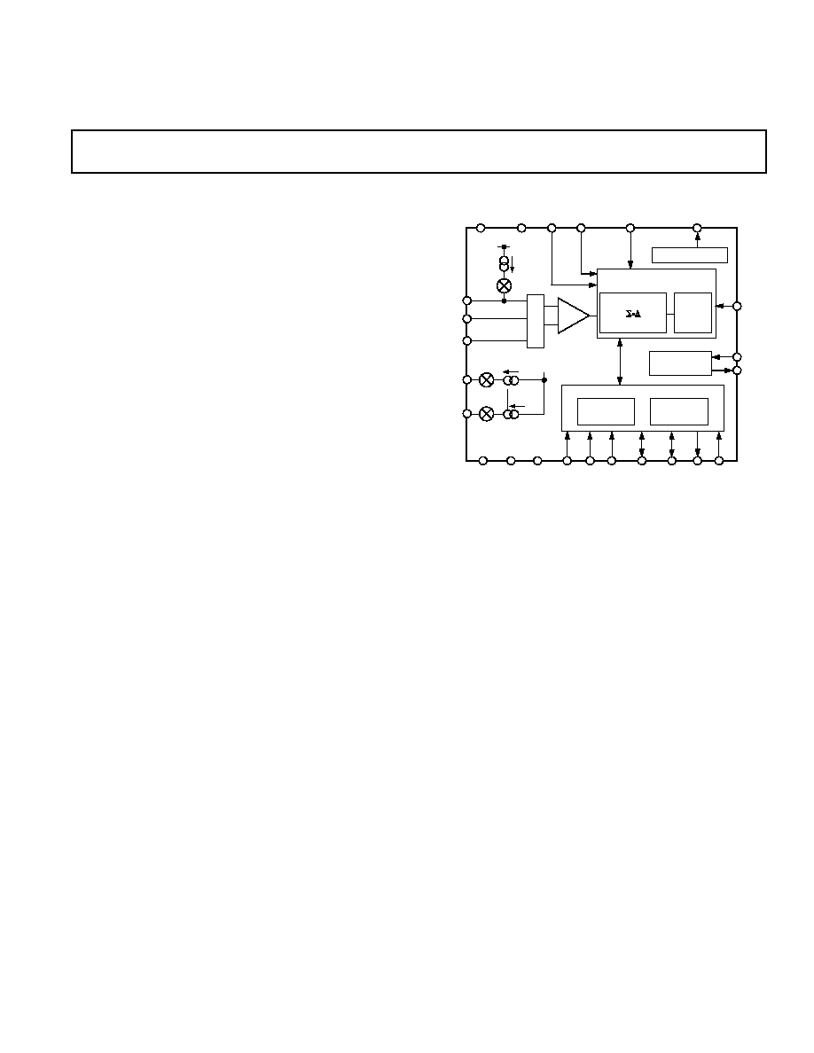
FUNCTIONAL BLOCK DIAGRAM
FEATURES
Charge Balancing ADC
24 Bits No Missing Codes
0.0015% Nonlinearity
Two-Channel Programmable Gain Front End
Gains from 1 to 128
One Differential Input
One Single-Ended Input
Low-Pass Filter with Programmable Filter Cutoffs
Ability to Read/Write Calibration Coefficients
RTD Excitation Current Sources
Bidirectional Microcontroller Serial Interface
Internal/External Reference Option
Single or Dual Supply Operation
Low Power (25 mW typ) with Power-Down Mode
(7 mW typ)
APPLICATIONS
RTD Transducers
Process Control
Smart Transmitters
Portable Industrial Instruments
LC
2
MOS Signal Conditioning ADC
with RTD Excitation Currents
REV. F
Information furnished by Analog Devices is believed to be accurate and
reliable. However, no responsibility is assumed by Analog Devices for its
use, nor for any infringements of patents or other rights of third parties
which may result from its use. No license is granted by implication or
otherwise under any patent or patent rights of Analog Devices.
GENERAL DESCRIPTION
The AD7711 is a complete analog front end for low frequency
measurement applications. The device accepts low level signals
directly from a transducer and outputs a serial digital word. It
employs a sigma-delta conversion technique to realize up to
24 bits of no missing codes performance. The input signal is
applied to a proprietary programmable gain front end based
around an analog modulator. The modulator output is pro-
cessed by an on-chip digital filter. The first notch of this digital
filter can be programmed via the on-chip control register allow-
ing adjustment of the filter cutoff and settling time.
The part features one differential analog input and one single
ended analog input as well as a differential reference input.
Normally, one of the input channels will be used as the main
channel with the second channel used as an auxiliary input to
periodically measure a second voltage. It can be operated from a
single supply (by tying the V
SS
pin to AGND) provided that the
input signals on the analog inputs are more positive than
30 mV. By taking the V
SS
pin negative, the part can convert
signals down to V
REF
on its inputs. The part provides two
current sources that can be used to provide excitation in three-
wire and four-wire RTD configurations. The AD7711 thus
performs all signal conditioning and conversion for a single or
dual channel system.
The AD7711 is ideal for use in smart, microcontroller based
systems. Gain settings, signal polarity, input channel selection
AD7711*
and RTD current control can be configured in software using
the bidirectional serial port. The AD7711 contains self-
calibration, system calibration and background calibration
options and also allows the user to read and write the on-chip
calibration registers.
CMOS construction ensures low power dissipation, and a soft-
ware programmable power-down mode reduces the standby
power consumption to only 7 mW typical. The part is available
in a 24-lead, 0.3 inch wide, plastic and hermetic dual-in-line
package (DIP) as well as a 24-lead small outline (SOIC)
package.
PRODUCT HIGHLIGHTS
1. The programmable gain front end allows the AD7711 to
accept input signals directly from an RTD transducer,
removing a considerable amount of signal conditioning.
On-chip current sources provide excitation for three-wire and
four-wire RTD configurations.
2. No Missing Codes ensure true, usable, 23-bit dynamic range
coupled with excellent
±
0.0015% accuracy. The effects of
temperature drift are eliminated by on-chip self-calibration,
which removes zero-scale and full-scale errors.
3. The AD7711 is ideal for microcontroller or DSP processor
applications with an on-chip control register which allows
control over filter cutoff, input gain, channel selection, signal
polarity, RTD current control and calibration modes.
4. The AD7711 allows the user to read and to write the on-chip
calibration registers. This means that the microcontroller has
much greater control over the calibration procedure.
One Technology Way, P.O. Box 9106, Norwood, MA 02062-9106, U.S.A.
Tel: 781/329-4700
World Wide Web Site: http://www.analog.com
Fax: 781/326-8703
© Analog Devices, Inc., 1998
*Protected by U.S. Patent No. 5,134,401.
CLOCK
GENERATION
SERIAL INTERFACE
CONTROL
REGISTER
OUTPUT
REGISTER
CHARGE-BALANCING A/D
CONVERTER
AUTO-ZEROED
MODULATOR
DIGITAL
FILTER
AD7711
M
U
X
AGND DGND
MODE SDATA SCLK
A0
MCLK
OUT
MCLK
IN
AIN1(+)
AIN1()
REF
IN ()
REF
IN (+)
SYNC
4.5 A
A = 1 128
DRDY
TFS
RFS
REF OUT
2.5V REFERENCE
200 A
AIN2
V
SS
V
BIAS
AV
DD
DV
DD
PGA
AV
DD
RTD2
200 A
RTD1
AV
DD
Parameter
A, S Versions
1
Units
Conditions/Comments
STATIC PERFORMANCE
No Missing Codes
24
Bits min
Guaranteed by Design. For Filter Notches
60 Hz
22
Bits min
For Filter Notch = 100 Hz
18
Bits min
For Filter Notch = 250 Hz
15
Bits min
For Filter Notch = 500 Hz
12
Bits min
For Filter Notch = 1 kHz
Output Noise
See Tables I & II
Depends on Filter Cutoffs and Selected Gain
Integral Nonlinearity @ +25
°
C
±
0.0015
% FSR max
Filter Notches
60 Hz
T
MIN
to T
MAX
±
0.003
% FSR max
Typically
±
0.0003%
Positive Full-Scale Error
2, 3
See Note 4
Excluding Reference
Full-Scale Drift
5
1
µ
V/
°
C typ
Excluding Reference. For Gains of 1, 2
0.3
µ
V/
°
C typ
Excluding Reference. For Gains of 4, 8, 16, 32, 64, 128
Unipolar Offset Error
2
See Note 4
Unipolar Offset Drift
5
0.5
µ
V/
°
C typ
For Gains of 1, 2
0.25
µ
V/
°
C typ
For Gains of 4, 8, 16, 32, 64, 128
Bipolar Zero Error
2
See Note 4
Bipolar Zero Drift
5
0.5
µ
V/
°
C typ
For Gains of 1, 2
0.25
µ
V/
°
C typ
For Gains of 4, 8, 16, 32, 64, 128
Gain Drift
2
ppm/
°
C typ
Bipolar Negative Full-Scale Error
2
@ +25
°
C
±
0.003
% FSR max
Excluding Reference
T
MIN
to T
MAX
±
0.006
% FSR max
Typically
±
0.0006%
Bipolar Negative Full-Scale Drift
5
1
µ
V/
°
C typ
Excluding Reference. For Gains of 1, 2
0.3
µ
V/
°
C typ
Excluding Reference. For Gains of 4, 8, 16, 32, 64, 128
ANALOG INPUTS/REFERENCE INPUTS
Normal-Mode 50 Hz Rejection
6
100
dB min
For Filter Notches of 10, 25, 50 Hz,
±
0.02
×
f
NOTCH
Normal-Mode 60 Hz Rejection
6
100
dB min
For Filter Notches of 10, 30, 60 Hz,
±
0.02
×
f
NOTCH
DC Input Leakage Current
@ +25
°
C
6
10
pA max
T
MIN
to T
MAX
1
nA max
Sampling Capacitance
6
20
pF max
AIN1/REF IN
Common-Mode Rejection (CMR)
100
dB min
At DC
Common-Mode 50 Hz Rejection
6
150
dB min
For Filter Notches of 10, 25, 50 Hz,
±
0.02
×
f
NOTCH
Common-Mode 60 Hz Rejection
6
150
dB min
For Filter Notches of 10, 30, 60 Hz,
±
0.02
×
f
NOTCH
Common-Mode Voltage Range
7
V
SS
to AV
DD
V min to V max
Analog Inputs
8
Input Voltage Range
9
For Normal Operation. Depends on Gain Selected
0 to +V
REF
10
max
Unipolar Input Range (B/U Bit of Control Register = 1)
±
V
REF
max
Bipolar Input Range (B/U Bit of Control Register = 0)
Input Sampling Rate, f
S
See Table III
AIN2 Offset Error
2.5
mV max
Removed by System Calibrations but not by Self-Calibration
AIN2 Offset Drift
1.5
µ
V/
°
C typ
Reference Inputs
REF IN(+) REF IN() Voltage
11
+2.5 to +5
V min to V max
For Specified Performance. Part Is Functional with
Lower V
REF
Voltages
Input Sampling Rate, f
S
f
CLK IN
/256
REFERENCE OUTPUT
Output Voltage
2.5
V nom
Initial Tolerance @ +25
°
C
±
1
% max
Drift
20
ppm/
°
C typ
Output Noise
30
µ
V typ
pk-pk Noise. 0.1 Hz to 10 Hz Bandwidth
Line Regulation (AV
DD
)
1
mV/V max
Load Regulation
1.5
mV/mA max
Maximum Load Current 1 mA
External Current
1
mA max
NOTES
1
Temperature range is as follows: A Version = 40
°
C to +85
°
C; S Version = 55
°
C to +125
°
C. See also Note 16.
2
Applies after calibration at the temperature of interest.
3
Positive full-scale error applies to both unipolar and bipolar input ranges.
4
These errors will be of the order of the output noise of the part as shown in Table I after system calibration. These errors will be 20
µ
V typical after self-calibration or
background calibration.
5
Recalibration at any temperature or use of the background calibration mode will remove these drift errors.
6
These numbers are guaranteed by design and/or characterization.
7
This common-mode voltage range is allowed, provided that the input voltage on AIN(+) and AIN() does not exceed AV
DD
+ 30 mV and V
SS
30 mV.
8
The analog inputs present a very high impedance dynamic load which varies with clock frequency and input sample rate. The maximum recommended source
resistance depends on the selected gain (see Tables IV and V).
9
The analog input voltage range on the AIN1(+) input is given here with respect to the voltage on the AIN1() input. The input voltage range on the AIN2 input is
with respect to AGND. The absolute voltage on the analog inputs should not go more positive than A V
DD
+ 30 mV or go more negative than V
SS
30 mV.
10
V
REF
= REF IN(+) REF IN().
11
The reference input voltage range may be restricted by the input voltage range requirement on the V
BIAS
input.
AD7711SPECIFICATIONS
2
REV. F
(AV
DD
= +5 V
5%; DV
DD
= +5 V 5%; V
SS
= 0 V or 5 V 5%; REF IN(+) =
+2.5 V; REF IN() = AGND; MCLK IN = 10 MHz unless otherwise stated. All specifications T
MIN
to T
MAX
unless otherwise noted.)
Parameter
A, S Versions
1
Units
Conditions/Comments
V
BIAS
INPUT
12
Input Voltage Range
AV
DD
0.85
×
V
REF
See V
BIAS
Input Section
or AV
DD
3.5
V max
Whichever Is Smaller; +5 V/5 V or +10 V/0 V
Nominal AV
DD
/V
SS
or AV
DD
2.1
V max
Whichever Is Smaller; +5 V/0 V Nominal AV
DD
/V
SS
V
SS
+ 0.85
×
V
REF
See V
BIAS
Input Section
or V
SS
+ 3
V min
Whichever Is Greater; +5 V/5 V or +10 V/0 V
Nominal AV
DD
/V
SS
or V
SS
+ 2.1
V min
Whichever Is Greater; +5 V/0 V Nominal AV
DD
/V
SS
V
BIAS
Rejection
65 to 85
dB typ
Increasing with Gain
LOGIC INPUTS
Input Current
±
10
µ
A max
All Inputs except MCLK IN
V
INL
, Input Low Voltage
0.8
V max
V
INH
, Input High Voltage
2.0
V min
MCLK IN Only
V
INL
, Input Low Voltage
0.8
V max
V
INH
, Input High Voltage
3.5
V min
LOGIC OUTPUTS
V
OL
, Output Low Voltage
0.4
V max
I
SINK
= 1.6 mA
V
OH
, Output High Voltage
4.0
V min
I
SOURCE
= 100
µ
A
Floating State Leakage Current
±
10
µ
A max
Floating State Output Capacitance
13
9
pF typ
TRANSDUCER BURNOUT
Current
4.5
µ
A nom
Initial Tolerance @ +25
°
C
±
10
% typ
Drift
0.1
%/
°
C typ
RTD EXCITATION CURRENTS (RTD1, RTD2)
Output Current
200
µ
A nom
Initial Tolerance @ +25
°
C
±
20
% max
Drift
20
ppm/
°
C typ
Initial Matching @ +25
°
C
±
1
% max
Matching Between RTD1 and RTD2 Currents
Drift Matching
3
ppm/
°
C typ
Matching Between RTD1 and RTD2 Current Drift
Line Regulation (AV
DD
)
200
nA/V max
AV
DD
= +5 V
Load Regulation
200
nA/V max
Output Compliance
AV
DD
2
V max
SYSTEM CALIBRATION
Positive Full-Scale Calibration Limit
14
(1.05
×
V
REF
)/GAIN
V max
GAIN Is the Selected PGA Gain (Between 1 and 128)
Negative Full-Scale Calibration Limit
14
(1.05
×
V
REF
)/GAIN
V max
GAIN Is the Selected PGA Gain (Between 1 and 128)
Offset Calibration Limit
15
(1.05
×
V
REF
)/GAIN
V max
GAIN Is the Selected PGA Gain (Between 1 and 128)
Input Span
15
0.8
×
V
REF
/GAIN
V min
GAIN Is the Selected PGA Gain (Between 1 and 128)
(2.1
×
V
REF
)/GAIN
V max
GAIN Is the Selected PGA Gain (Between 1 and 128)
NOTES
12
The AD7711 is tested with the following V
BIAS
voltages. With AV
DD
= +5 V and V
SS
= 0 V, V
BIAS
= +2.5 V; with AV
DD
= +10 V and V
SS
= 0 V, V
BIAS
= +5 V and
with AV
DD
= +5 V and V
SS
= 5 V, V
BIAS
= 0 V.
13
Guaranteed by design, not production tested.
14
After calibration, if the analog input exceeds positive full scale, the converter will output all 1s. If the analog input is less than negative full scale, then the device will
output all 0s.
15
These calibration and span limits apply provided the absolute voltage on the analog inputs does not exceed AV
DD
+ 30 mV or go more negative than V
SS
30 mV.
The offset calibration limit applies to both the unipolar zero point and the bipolar zero point.
3
REV. F
AD7711
ORDERING GUIDE
Model
Temperature Range
Package Option*
AD7711AN
40
°
C to +85
°
C
N-24
AD7711AR
40
°
C to +85
°
C
R-24
AD7711AQ
40
°
C to +85
°
C
Q-24
AD7711SQ
55
°
C to +125
°
C
Q-24
EVAL-AD7711EB
Evaluation Board
*N = Plastic DIP, Q = Cerdip; R = SOIC.
Parameter
A, S Versions
1
Units
Conditions/Comments
POWER REQUIREMENTS
Power Supply Voltages
AV
DD
Voltage
16
+5 to +10
V nom
±
5% for Specified Performance
DV
DD
Voltage
17
+5
V nom
±
5% for Specified Performance
AV
DD
V
SS
Voltage
+10.5
V max
For Specified Performance
Power Supply Currents
AV
DD
Current
4
mA max
DV
DD
Current
4.5
mA max
V
SS
Current
1.5
mA max
V
SS
= 5 V
Power Supply Rejection
18
Rejection w.r.t. AGND; Assumes V
BIAS
Is Fixed
Positive Supply (AV
DD
and DV
DD
)
See Note 19
dB typ
Negative Supply (V
SS
)
90
dB typ
Power Dissipation
Normal Mode
45
mW max
AV
DD
= DV
DD
= +5 V, V
SS
= 0 V; Typically 25 mW
52.5
mW max
AV
DD
= DV
DD
= +5 V, V
SS
= 5 V; Typically 30 mW
Standby (Power-Down) Dissipation
15
mW max
AV
DD
= DV
DD
= +5 V, V
SS
= 0 V or 5 V; Typically 7 mW
NOTES
16
The AD7711 is specified with a 10 MHz clock for AV
DD
voltages of +5 V
±
5%. It is specified with an 8 MHz clock for AV
DD
voltages greater than 5.25 V and less
than 10.5 V.
17
The
±
5% tolerance on the DV
DD
input is allowed provided that DV
DD
does not exceed AV
DD
by more than 0.3 V.
18
Measured at dc and applies in the selected passband. PSRR at 50 Hz will exceed 120 dB with filter notches of 10 Hz, 25 Hz or 50 Hz. PSRR at 60 Hz will exceed
120 dB with filter notches of 10 Hz, 30 Hz or 60 Hz.
19
PSRR depends on gain: Gain of 1 = 70 dB typ; Gain of 2: 75 dB typ; Gain of 4 = 80 dB typ; Gains of 8 to 128 = 85 dB typ. These numbers can be improved (to
95 dB typ) by deriving the V
BIAS
voltage (via Zener diode or reference) from the AV
DD
supply.
Specifications subject to change without notice.
AD7711SPECIFICATIONS
REF OUT to AGND . . . . . . . . . . . . . . . . . . . . 0.3 V to AV
DD
Digital Input Voltage to DGND . . . . . 0.3 V to AV
DD
+ 0.3 V
Digital Output Voltage to DGND . . . 0.3 V to DV
DD
+ 0.3 V
Operating Temperature Range
Commercial (A Version) . . . . . . . . . . . . . . . . 40
°
C to +85
°
C
Extended (S Version) . . . . . . . . . . . . . . . . . 55
°
C to +125
°
C
Storage Temperature Range . . . . . . . . . . . . . 65
°
C to +150
°
C
Lead Temperature (Soldering, 10 secs) . . . . . . . . . . . . +300
°
C
Power Dissipation (Any Package) to +75
°
C . . . . . . . . 450 mW
*Stresses above those listed under Absolute Maximum Ratings may cause perma-
nent damage to the device. This is a stress rating only; functional operation of the
device at these or any other conditions above those listed in the operational
sections of the specification is not implied. Exposure to absolute maximum rating
conditions for extended periods may affect device reliability.
ABSOLUTE MAXIMUM RATINGS*
(T
A
= +25
°
C, unless otherwise noted)
AV
DD
to DV
DD
. . . . . . . . . . . . . . . . . . . . . . . 0.3 V to +12 V
AV
DD
to V
SS
. . . . . . . . . . . . . . . . . . . . . . . . . . 0.3 V to +12 V
AV
DD
to AGND . . . . . . . . . . . . . . . . . . . . . . 0.3 V to +12 V
AV
DD
to DGND . . . . . . . . . . . . . . . . . . . . . . 0.3 V to +12 V
DV
DD
to AGND . . . . . . . . . . . . . . . . . . . . . . . 0.3 V to +6 V
DV
DD
to DGND . . . . . . . . . . . . . . . . . . . . . . . 0.3 V to +6 V
V
SS
to AGND . . . . . . . . . . . . . . . . . . . . . . . . . +0.3 V to 6 V
V
SS
to DGND . . . . . . . . . . . . . . . . . . . . . . . . . +0.3 V to 6 V
Analog Input Voltage to AGND
. . . . . . . . . . . . . . . . . . . . . . . . . V
SS
0.3 V to AV
DD
+ 0.3 V
Reference Input Voltage to AGND
. . . . . . . . . . . . . . . . . . . . . . . . . V
SS
0.3 V to AV
DD
+ 0.3 V
REV. F
4
CAUTION
ESD (electrostatic discharge) sensitive device. The digital control inputs are diode protected;
however, permanent damage may occur on unconnected devices subject to high energy electro-
static fields. Unused devices must be stored in conductive foam or shunts. The protective foam
should be discharged to the destination socket before devices are inserted.
WARNING!
ESD SENSITIVE DEVICE
2
AD7711
5
REV. F
TIMING CHARACTERISTICS
1, 2
Limit at T
MIN
, T
MAX
Parameter
(A, S Versions)
Units
Conditions/Comments
f
CLK IN
4, 5
400
kHz min
Master Clock Frequency: Crystal Oscillator or Externally
Supplied for Specified Performance
10
MHz max
t
CLK IN LO
0.4
×
t
CLK IN
ns min
Master Clock Input Low Time; t
CLK IN
= 1/f
CLK IN
t
CLK IN HI
0.4
×
t
CLK IN
ns min
Master Clock Input High Time
t
r
6
50
ns max
Digital Output Rise Time. Typically 20 ns
t
f
6
50
ns max
Digital Output Fall Time. Typically 20 ns
t
1
1000
ns min
SYNC Pulsewidth
Self-Clocking Mode
t
2
0
ns min
DRDY to RFS Setup Time
t
3
0
ns min
DRDY to RFS Hold Time
t
4
2
×
t
CLK IN
ns min
A0 to
RFS Setup Time
t
5
0
ns min
A0 to
RFS Hold Time
t
6
4
×
t
CLK IN
+ 20
ns max
RFS Low to SCLK Falling Edge
t
7
7
4
×
t
CLK IN
+ 20
ns max
Data Access Time (
RFS Low to Data Valid)
t
8
7
t
CLK IN
/2
ns min
SCLK Falling Edge to Data Valid Delay
t
CLK IN
/2
+ 30
ns max
t
9
t
CLK IN
/2
ns nom
SCLK High Pulsewidth
t
10
3
×
t
CLK IN
/2
ns nom
SCLK Low Pulsewidth
t
14
50
ns min
A0 to
TFS Setup Time
t
15
0
ns min
A0 to
TFS Hold Time
t
16
4
×
t
CLK IN
+ 20
ns max
TFS to SCLK Falling Edge Delay Time
t
17
4
×
t
CLK IN
ns min
TFS to SCLK Falling Edge Hold Time
t
18
0
ns min
Data Valid to SCLK Setup Time
t
19
10
ns min
Data Valid to SCLK Hold Time
(DV
DD
= +5 V 5%; AV
DD
= +5 V or +10 V
3
5%; V
SS
= 0 V or 5 V 10%; AGND = DGND =
0 V; f
CLK IN
= 10 MHz; Input Logic 0 = 0 V, Logic 1 = DV
DD
, unless otherwise noted.)