 | ÐлекÑÑоннÑй компоненÑ: AD7730 | СкаÑаÑÑ:  PDF PDF  ZIP ZIP |
Äîêóìåíòàöèÿ è îïèñàíèÿ www.docs.chipfind.ru
REV. A
Information furnished by Analog Devices is believed to be accurate and
reliable. However, no responsibility is assumed by Analog Devices for its
use, nor for any infringements of patents or other rights of third parties
which may result from its use. No license is granted by implication or
otherwise under any patent or patent rights of Analog Devices.
a
AD7730/AD7730L
One Technology Way, P.O. Box 9106, Norwood, MA 02062-9106, U.S.A.
Tel: 781/329-4700
World Wide Web Site: http://www.analog.com
Fax: 781/326-8703
© Analog Devices, Inc., 1998
Bridge Transducer ADC
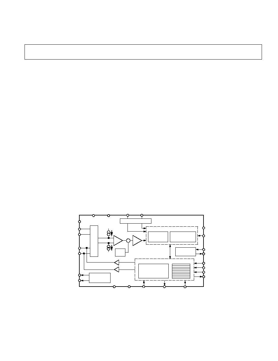
FUNCTIONAL BLOCK DIAGRAM
KEY FEATURES
Resolution of 230,000 Counts (Peak-to-Peak)
Offset Drift: 5 nV/ C
Gain Drift: 2 ppm/ C
Line Frequency Rejection: >150 dB
Buffered Differential Inputs
Programmable Filter Cutoffs
Specified for Drift Over Time
Operates with Reference Voltages of 1 V to 5 V
ADDITIONAL FEATURES
Two-Channel Programmable Gain Front End
On-Chip DAC for Offset/TARE Removal
FASTStepTM Mode
AC or DC Excitation
Single Supply Operation
APPLICATIONS
Weigh Scales
Pressure Measurement
GENERAL DESCRIPTION
The AD7730 is a complete analog front end for weigh-scale and
pressure measurement applications. The device accepts low-
level signals directly from a transducer and outputs a serial
digital word. The input signal is applied to a proprietary pro-
grammable gain front end based around an analog modulator.
FASTStep is a trademark of Analog Devices, Inc.
SIGMA-
DELTA
MODULATOR
AD7730
6-BIT
DAC
SERIAL INTERFACE
AND CONTROL LOGIC
REGISTER BANK
CLOCK
GENERATION
PROGRAMMABLE
DIGITAL
FILTER
SIGMA-DELTA A/D CONVERTER
BUFFER
PGA
100nA
AGND
100nA
AV
DD
VBIAS
AIN1(+)
AIN1()
AIN2(+)/D1
AIN2()/D0
ACX
ACX
STANDBY
SYNC
MCLK IN
MCLK OUT
SCLK
CS
DIN
DOUT
RESET
RDY
POL
DGND
AGND
AV
DD
DV
DD
REF IN() REF IN(+)
MUX
REFERENCE DETECT
AC
EXCITATION
CLOCK
CALIBRATION
MICROCONTROLLER
+
+/
The modulator output is processed by a low pass programmable
digital filter, allowing adjustment of filter cutoff, output rate and
settling time.
The part features two buffered differential programmable gain
analog inputs as well as a differential reference input. The part
operates from a single +5 V supply. It accepts four unipolar
analog input ranges: 0 mV to +10 mV, +20 mV, +40 mV and
+80 mV and four bipolar ranges:
±
10 mV,
±
20 mV,
±
40 mV
and
±
80 mV. The peak-to-peak resolution achievable directly
from the part is 1 in 230,000 counts. An on-chip 6-bit DAC
allows the removal of TARE voltages. Clock signals for synchro-
nizing ac excitation of the bridge are also provided.
The serial interface on the part can be configured for three-wire
operation and is compatible with microcontrollers and digital
signal processors. The AD7730 contains self-calibration and
system calibration options, and features an offset drift of less
than 5 nV/
°
C and a gain drift of less than 2 ppm/
°
C.
The AD7730 is available in a 24-pin plastic DIP, a 24-lead
SOIC and 24-lead TSSOP package. The AD7730L is available
in a 24-lead SOIC and 24-lead TSSOP package.
NOTE
The description of the functions and operation given in this data
sheet apply to both the AD7730 and AD7730L. Specifications
and performance parameters differ for the parts. Specifications
for the AD7730L are outlined in Appendix A.

2
REV. A
Parameter
B Version
1
Units
Conditions/Comments
STATIC PERFORMANCE (CHP = 1)
No Missing Codes
2
24
Bits min
Output Noise and Update Rates
2
See Tables I & II
Integral Nonlinearity
18
ppm of FSR max
Offset Error
2
See Note 3
Offset Error and Offset Drift Refer to Both
Offset Drift vs. Temperature
2
5
nV/
°
C typ
Unipolar Offset and Bipolar Zero Errors
Offset Drift vs. Time
4
25
nV/1000 Hours typ
Positive Full-Scale Error
2, 5
See Note 3
Positive Full-Scale Drift vs Temp
2, 6, 7
2
ppm of FS/
°
C max
Positive Full-Scale Drift vs Time
4
10
ppm of FS/1000 Hours typ
Gain Error
2, 8
See Note 3
Gain Drift vs. Temperature
2, 6, 9
2
ppm/
°
C max
Gain Drift vs. Time
4
10
ppm/1000 Hours typ
Bipolar Negative Full-Scale Error
2
See Note 3
Negative Full-Scale Drift vs. Temp
2, 6
2
ppm of FS/
°
C max
Power Supply Rejection
120
dB typ
Measured with Zero Differential Voltage
Common-Mode Rejection (CMR)
120
dB min
At DC. Measured with Zero Differential Voltage
Analog Input DC Bias Current
2
50
nA max
Analog Input DC Bias Current Drift
2
100
pA/
°
C typ
Analog Input DC Offset Current
2
10
nA max
Analog Input DC Offset Current Drift
2
50
pA/
°
C typ
STATIC PERFORMANCE (CHP = 0)
2
No Missing Codes
24
Bits min
SKIP = 0
10
Output Noise and Update Rates
See Tables III & IV
Integral Nonlinearity
18
ppm of FSR max
Offset Error
See Note 3
Offset Error and Offset Drift Refer to Both
Offset Drift vs. Temperature
6
0.5
µ
V/
°
C typ
Unipolar Offset and Bipolar Zero Errors
Offset Drift vs. Time
4
2.5
µ
V/1000 Hours typ
Positive Full-Scale Error
5
See Note 3
Positive Full-Scale Drift vs. Temp
6, 7
0.6
µ
V/
°
C typ
Positive Full-Scale Drift vs. Time
4
3
µ
V/1000 Hours typ
Gain Error
8
See Note 3
Gain Drift vs. Temperature
6, 9
2
ppm/
°
C typ
Gain Drift vs. Time
4
10
ppm/1000 Hours typ
Bipolar Negative Full-Scale Error
See Note 3
Negative Full-Scale Drift vs. Temp
0.6
µ
V/
°
C typ
Power Supply Rejection
90
dB typ
Measured with Zero Differential Voltage
Common-Mode Rejection (CMR) on AIN 100
dB typ
At DC. Measured with Zero Differential Voltage
CMR on REF IN
120
dB typ
At DC. Measured with Zero Differential Voltage
Analog Input DC Bias Current
60
nA max
Analog Input DC Bias Current Drift
150
pA/
°
C typ
Analog Input DC Offset Current
30
nA max
Analog Input DC Offset Current Drift
100
pA/
°
C typ
ANALOG INPUTS/REFERENCE INPUTS
Normal-Mode 50 Hz Rejection
2
88
dB min
From 49 Hz to 51 Hz
Normal-Mode 60 Hz Rejection
2
88
dB min
From 59 Hz to 61 Hz
Common-Mode 50 Hz Rejection
2
120
dB min
From 49 Hz to 51 Hz
Common-Mode 60 Hz Rejection
2
120
dB min
From 59 Hz to 61 Hz
Analog Inputs
Differential Input Voltage Ranges
11
Assuming 2.5 V or 5 V Reference with
HIREF Bit Set Appropriately
0 to +10 or
±
10
mV nom
Gain = 250
0 to +20 or
±
20
mV nom
Gain = 125
0 to +40 or
±
40
mV nom
Gain = 62.5
0 to +80 or
±
80
mV nom
Gain = 31.25
Absolute/Common-Mode Voltage
12
AGND + 1.2 V
V min
AV
DD
0.95 V
V max
Reference Input
REF IN(+) REF IN() Voltage
+2.5
V nom
HIREF Bit of Mode Register = 0
REF IN(+) REF IN() Voltage
+5
V nom
HIREF Bit of Mode Register = 1
Absolute/Common-Mode Voltage
13
AGND 30 mV
V min
AV
DD
+ 30 mV
V max
NO REF Trigger Voltage
0.3
V min
NO REF Bit Active If V
REF
Below This Voltage
0.65
V max
NO REF Bit Inactive If V
REF
Above This Voltage
AD7730SPECIFICATIONS
(AV
DD
= +5 V, DV
DD
= +3 V or +5 V; REF IN(+) = AV
DD
; REF IN() = AGND = DGND =
0 V; f
CLK IN
= 4.9152 MHz. All specifications T
MIN
to T
MAX
unless otherwise noted.)

3
REV. A
AD7730/AD7730L
Parameter
B Version
1
Units
Conditions/Comments
LOGIC INPUTS
Input Current
±
10
µ
A max
All Inputs Except SCLK and MCLK IN
V
INL
, Input Low Voltage
0.8
V max
DV
DD
= +5 V
V
INL
, Input Low Voltage
0.4
V max
DV
DD
= +3 V
V
INH
, Input High Voltage
2.0
V min
SCLK Only (Schmitt Triggered Input)
V
T+
1.4/3
V min to V max
DV
DD
= +5 V
V
T+
1/2.5
V min to V max
DV
DD
= +3 V
V
T
0.8/1.4
V min to V max
DV
DD
= +5 V
V
T
0.4/1.1
V min to V max
DV
DD
= +3 V
V
T+
V
T
0.4/0.8
V min to V max
DV
DD
= +5 V
V
T+
V
T
0.4/0.8
V min to V max
DV
DD
= +3 V
MCLK IN Only
V
INL
, Input Low Voltage
0.8
V max
DV
DD
= +5 V
V
INL
, Input Low Voltage
0.4
V max
DV
DD
= +3 V
V
INH
, Input High Voltage
3.5
V min
DV
DD
= +5 V
V
INH
, Input High Voltage
2.5
V min
DV
DD
= +3 V
LOGIC OUTPUTS (Including MCLK OUT)
V
OL
, Output Low Voltage
I
SINK
= 800
µ
A Except for MCLK OUT
14
;
0.4
V max
V
DD
15
= +5 V
V
OL
, Output Low Voltage
I
SINK
= 100
µ
A Except for MCLK OUT
14
;
0.4
V max
V
DD
15
= +3 V
V
OH
, Output High Voltage
I
SOURCE
= 200
µ
A Except for MCLK OUT
14
;
4.0
V min
V
DD
15
= +5 V
V
OH
, Output High Voltage
I
SOURCE
= 100
µ
A Except for MCLK OUT
14
;
V
DD
0.6 V
V min
V
DD
15
= +3 V
Floating State Leakage Current
±
10
µ
A max
Floating State Output Capacitance
2
6
pF typ
TRANSDUCER BURNOUT
AIN1(+) Current
100
nA nom
AIN1() Current
100
nA nom
Initial Tolerance @ 25
°
C
±
10
% typ
Drift
2
0.1
%/
°
C typ
OFFSET (TARE) DAC
Resolution
6
Bit
LSB Size
2.3/2.6
mV min/mV max
2.5 mV Nominal with 5 V Reference (REF IN/2000)
DAC Drift
16
2.5
ppm/
°
C max
DAC Drift vs. Time
4, 16
25
ppm/1000 Hours typ
Differential Linearity
0.25/+0.75
LSB max
Guaranteed Monotonic
SYSTEM CALIBRATION
Positive Full-Scale Calibration Limit
17
1.05
×
FS
V max
FS Is the Nominal Full-Scale Voltage
(10 mV, 20 mV, 40 mV or 80 mV)
Negative Full-Scale Calibration Limit
17
1.05
×
FS
V max
Offset Calibration Limit
18
1.05
×
FS
V max
Input Span
17
0.8
×
FS
V min
2.1
×
FS
V max
POWER REQUIREMENTS
Power Supply Voltages
AV
DD
AGND Voltage
+4.75 to +5.25
V min to V max
DV
DD
Voltage
+2.7 to +5.25
V min to V max
With AGND = 0 V
Power Supply Currents
External MCLK. Digital I/Ps = 0 V or DV
DD
AV
DD
Current (Normal Mode)
10.3
mA max
All Input Ranges Except 0 mV to +10 mV and
±
10 mV
AV
DD
Current (Normal Mode)
22.3
mA max
Input Ranges of 0 mV to +10 mV and
±
10 mV Only
DV
DD
Current (Normal Mode)
1.3
mA max
DV
DD
of 2.7 V to 3.3 V
DV
DD
Current (Normal Mode)
2.7
mA max
DV
DD
of 4.75 V to 5.25 V
AV
DD
+ DV
DD
Current (Standby Mode)
25
µ
A max
Typically 10
µ
A. External MCLK IN = 0 V or DV
DD
Power Dissipation
AV
DD
= DV
DD
= +5 V. Digital I/Ps = 0 V or DV
DD
Normal Mode
65
mW max
All Input Ranges Except 0 mV to +10 mV and
±
10 mV
125
mW max
Input Ranges of 0 mV to +10 mV and
±
10 mV Only
Standby Mode
125
µ
W max
Typically 50
µ
W. External MCLK IN = 0 V or DV
DD

AD7730/AD7730L
4
REV. A
NOTES
1
1
Temperature range: 40
°
C to +85
°
C.
1
2
Sample tested during initial release.
1
3
The offset (or zero) numbers with CHP = 1 are typically 3
µ
V precalibration. Internal zero-scale calibration reduces this by about 1
µ
V. Offset numbers with CHP = 0 can be up to
1 mV precalibration. Internal zero-scale calibration reduces this to 2
µ
V typical. System zero-scale calibration reduces offset numbers with CHP = 1 and CHP = 0 to the order of the
noise. Gain errors can be up to 3000 ppm precalibration with CHP = 0 and CHP = 1. Performing internal full-scale calibrations on the 80 mV range reduces the gain error to less than
100 ppm for the 80 mV and 40 mV ranges, to about 250 ppm for the 20 mV range and to about 500 ppm on the 10 mV range. System full-scale calibration reduces this to the order of
the noise. Positive and negative full-scale errors can be calculated from the offset and gain errors.
1
4
These numbers are generated during life testing of the part.
1
5
Positive Full-Scale Error includes Offset Errors (Unipolar Offset Error or Bipolar Zero Error) and applies to both unipolar and bipolar input ranges. See Terminology.
1
6
Recalibration at any temperature will remove these errors.
1
7
Full-Scale Drift includes Offset Drift (Unipolar Offset Drift or Bipolar Zero Drift) and applies to both unipolar and bipolar input ranges.
1
8
Gain Error is a measure of the difference between the measured and the ideal span between any two points in the transfer function. The two points used to calculate the gain
error are positive full scale and negative full scale. See Terminology.
1
9
Gain Error Drift is a span drift and is effectively the drift of the part if zero-scale calibrations only were performed.
10
No Missing Codes performance with CHP = 0 and SKIP = 1 is reduced below 24 bits for SF words lower than 180 decimal.
11
The analog input voltage range on the AIN1(+) and AIN2(+) inputs is given here with respect to the voltage on the AIN1() and AIN2() inputs respectively.
12
The common-mode voltage range on the input pairs applies provided the absolute input voltage specification is obeyed.
13
The common-mode voltage range on the reference input pair (REF IN(+) and REF IN()) applies provided the absolute input voltage specification is obeyed.
14
These logic output levels apply to the MCLK OUT output only when it is loaded with a single CMOS load.
15
V
DD
refers to DV
DD
for all logic outputs expect D0, D1, ACX and
ACX where it refers to AV
DD
. In other words, the output logic high for these four outputs is determined by AV
DD
.
16
This number represents the total drift of the channel with a zero input and the DAC output near full scale.
17
After calibration, if the input voltage exceeds positive full scale, the converter will output all 1s. If the input is less than negative full scale, the device outputs all 0s.
18
These calibration and span limits apply provided the absolute input voltage specification is obeyed. The offset calibration limit applies to both the unipolar zero point and the
bipolar zero point.
Specifications subject to change without notice.
TIMING CHARACTERISTICS
1, 2
Limit at T
MIN
to T
MAX
Parameter
(B Version)
Units
Conditions/Comments
Master Clock Range
1
MHz min
For Specified Performance
5
MHz max
t
1
50
ns min
SYNC Pulsewidth
t
2
50
ns min
RESET Pulsewidth
Read Operation
t
3
0
ns min
RDY to CS Setup Time
t
4
0
ns min
CS Falling Edge to SCLK Active Edge Setup Time
3
t
5
4
0
ns min
SCLK Active Edge to Data Valid Delay
3
60
ns max
DV
DD
= +4.75 V to +5.25 V
80
ns max
DV
DD
= +2.75 V to +3.3 V
t
5A
4, 5
0
ns min
CS Falling Edge to Data Valid Delay
60
ns max
DV
DD
= +4.75 V to +5.25 V
80
ns max
DV
DD
= +2.7 V to +3.3 V
t
6
100
ns min
SCLK High Pulsewidth
t
7
100
ns min
SCLK Low Pulsewidth
t
8
0
ns min
CS Rising Edge to SCLK Inactive Edge Hold Time
3
t
9
6
10
ns min
Bus Relinquish Time after SCLK Inactive Edge
3
80
ns max
t
10
100
ns max
SCLK Active Edge to
RDY High
3, 7
Write Operation
t
11
0
ns min
CS Falling Edge to SCLK Active Edge Setup Time
3
t
12
30
ns min
Data Valid to SCLK Edge Setup Time
t
13
25
ns min
Data Valid to SCLK Edge Hold Time
t
14
100
ns min
SCLK High Pulsewidth
t
15
100
ns min
SCLK Low Pulsewidth
t
16
0
ns min
CS Rising Edge to SCLK Edge Hold Time
NOTES
1
Sample tested during initial release to ensure compliance. All input signals are specified with tr = tf = 5 ns (10% to 90% of DV
DD
) and timed from a voltage level of 1.6 V.
2
See Figures 18 and 19.
3
SCLK active edge is falling edge of SCLK with POL = 1; SCLK active edge is rising edge of SCLK with POL = 0.
4
These numbers are measured with the load circuit of Figure 1 and defined as the time required for the output to cross the V
OL
or V
OH
limits.
5
This specification only comes into play if
CS goes low while SCLK is low (POL = 1) or if CS goes low while SCLK is high (POL = 0). It is primarily required for
interfacing to DSP machines.
6
These numbers are derived from the measured time taken by the data output to change 0.5 V when loaded with the circuit of Figure 1. The measured number is then
extrapolated back to remove effects of charging or discharging the 50 pF capacitor. This means that the times quoted in the timing characteristics are the true bus
relinquish times of the part and as such are independent of external bus loading capacitances.
7
RDY returns high after the first read from the device after an output update. The same data can be read again, if required, while RDY is high, although care should
be taken that subsequent reads do not occur close to the next output update.
(AV
DD
= +4.75 V to +5.25 V; DV
DD
= +2.7 V to +5.25 V; AGND = DGND = 0 V; f
CLK IN
= 4.9152 MHz;
Input Logic 0 = 0 V, Logic 1 = DV
DD
unless otherwise noted).
AD7730/AD7730L
REV. A
5
CAUTION
ESD (electrostatic discharge) sensitive device. Electrostatic charges as high as 4000 V readily
accumulate on the human body and test equipment and can discharge without detection.
Although the AD7730 features proprietary ESD protection circuitry, permanent damage may
occur on devices subjected to high energy electrostatic discharges. Therefore, proper ESD
precautions are recommended to avoid performance degradation or loss of functionality.
ABSOLUTE MAXIMUM RATINGS*
(T
A
= +25
°
C unless otherwise noted)
AV
DD
to AGND . . . . . . . . . . . . . . . . . . . . . . . 0.3 V to +7 V
AV
DD
to DGND . . . . . . . . . . . . . . . . . . . . . . . 0.3 V to +7 V
DV
DD
to AGND . . . . . . . . . . . . . . . . . . . . . . . 0.3 V to +7 V
DV
DD
to DGND . . . . . . . . . . . . . . . . . . . . . . . 0.3 V to +7 V
AGND to DGND . . . . . . . . . . . . . . . . . . . . . . 5 V to +0.3 V
AV
DD
to DV
DD
. . . . . . . . . . . . . . . . . . . . . . . . . 2 V to +5 V
Analog Input Voltage to AGND . . . . 0.3 V to AV
DD
+ 0.3 V
Reference Input Voltage to AGND . . 0.3 V to AV
DD
+ 0.3 V
AIN/REF IN Current (Indefinite) . . . . . . . . . . . . . . . . 30 mA
Digital Input Voltage to DGND . . . . 0.3 V to DV
DD
+ 0.3 V
Digital Output Voltage to DGND . . . 0.3 V to DV
DD
+ 0.3 V
Output Voltage (ACX,
ACX, D0, D1) to DGND
. . . . . . . . . . . . . . . . . . . . . . . . . . . . 0.3 V to AV
DD
+ 0.3 V
Operating Temperature Range
Industrial (B Version) . . . . . . . . . . . . . . . 40
°
C to +85
°
C
Storage Temperature Range . . . . . . . . . . . 65
°
C to +150
°
C
Junction Temperature . . . . . . . . . . . . . . . . . . . . . . . . +150
°
C
ORDERING GUIDE
Temperature
Package
Package
Model
Range
Description
Options
AD7730BN
40
°
C to +85
°
C
Plastic DIP
N-24
AD7730BR
40
°
C to +85
°
C
Small Outline
R-24
AD7730BRU
40
°
C to +85
°
C
Thin Shrink Small Outline
RU-24
EVAL-AD7730EB
Evaluation Board
AD7730LBR
40
°
C to +85
°
C
Small Outline
R-24
AD7730LBRU
40
°
C to +85
°
C
Thin Shrink Small Outline
RU-24
EVAL-AD7730LEB
Evaluation Board
Plastic DIP Package, Power Dissipation . . . . . . . 450 mW
JA
Thermal Impedance . . . . . . . . . . . . . . . . . 105
°
C/W
Lead Temperature (Soldering, 10 sec) . . . . . . . +260
°
C
TSSOP Package, Power Dissipation . . . . . . . . . . 450 mW
JA
Thermal Impedance . . . . . . . . . . . . . . . . . 128
°
C/W
Lead Temperature, Soldering
Vapor Phase (60 sec) . . . . . . . . . . . . . . . . . . +215
°
C
Infrared (15 sec) . . . . . . . . . . . . . . . . . . . . . . +220
°
C
SOIC Package, Power Dissipation . . . . . . . . . . . . 450 mW
JA
Thermal Impedance . . . . . . . . . . . . . . . . . . 75
°
C/W
Lead Temperature, Soldering
Vapor Phase (60 sec) . . . . . . . . . . . . . . . . . . +215
°
C
Infrared (15 sec) . . . . . . . . . . . . . . . . . . . . . . +220
°
C
*Stresses above those listed under Absolute Maximum Ratings may cause
permanent damage to the device. This is a stress rating only; functional
operation of the device at these or any other conditions above those listed in
the operational sections of this specification is not implied. Exposure to
absolute maximum rating conditions for extended periods may affect device
reliability.
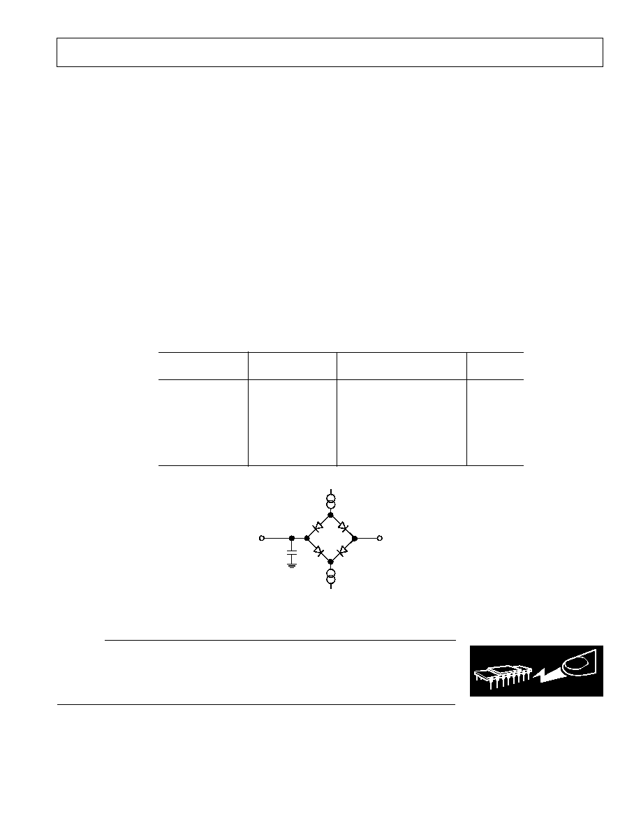
TO OUTPUT
PIN
50pF
I
SINK
(800 A AT DV
DD
= +5V
100 A AT DV
DD
= +3V)
+1.6V
I
SOURCE
(200 A AT DV
DD
= +5V
100 A AT DV
DD
= +3V)
Figure 1. Load Circuit for Access Time and Bus Relinquish Time
WARNING!
ESD SENSITIVE DEVICE