 | ÐлекÑÑоннÑй компоненÑ: AD779 | СкаÑаÑÑ:  PDF PDF  ZIP ZIP |
Äîêóìåíòàöèÿ è îïèñàíèÿ www.docs.chipfind.ru
FUNCTIONAL BLOCK DIAGRAM
REV. B
Information furnished by Analog Devices is believed to be accurate and
reliable. However, no responsibility is assumed by Analog Devices for its
use, nor for any infringements of patents or other rights of third parties
which may result from its use. No license is granted by implication or
otherwise under any patent or patent rights of Analog Devices.
a
14-Bit 128 kSPS
Complete Sampling ADC
AD779*
One Technology Way, P.O. Box 9106, Norwood, MA 02062-9106, U.S.A.
Tel: 617/329-4700
Fax: 617/326-8703
FEATURES
AC and DC Characterized and Specified (K, B, T
Grades)
128k Conversions per Second
1 MHz Full Power Bandwidth
500 kHz Full Linear Bandwidth
80 dB S/N+D (K, B, T Grades)
Twos Complement Data Format (Bipolar Mode)
Straight Binary Data Format (Unipolar Mode)
10 M Input Impedance
16-Bit Bus Interface (See AD679 for 8-Bit Interface)
Onboard Reference and Clock
10 V Unipolar or Bipolar Input Range
MIL-STD-883 Compliant Versions Available
PRODUCT DESCRIPTION
The AD779 is a complete, multipurpose 14-bit monolithic
analog-to-digital converter, consisting of a sample-hold amplifier
(SHA), a microprocessor compatible bus interface, a voltage
reference and clock generation circuitry.
The AD779 is specified for ac (or "dynamic") parameters such
as S/N+D ratio, THD and IMD which are important in signal
processing applications. In addition, the AD779K, B and T
grades are fully specified for dc parameters which are important
in measurement applications.
The 14 data bits are accessed by a 16-bit bus in a single read
operation. Data format is straight binary for unipolar mode and
twos complement binary for bipolar mode. The input has a full-
scale range of 10 V with a full power bandwidth of 1 MHz and a
full linear bandwidth of 500 kHz. High input impedance (10 M
)
allows direct connection to unbuffered sources without signal
degradation.
This product is fabricated on Analog Devices' BiMOS process,
combining low power CMOS logic with high precision, low
noise bipolar circuits; laser-trimmed thin-film resistors provide
high accuracy. The converter utilizes a recursive subranging
algorithm which includes error correction and flash converter
circuitry to achieve high speed and resolution.
The AD779 operates from +5 V and
±
12 V supplies and
dissipates 560 mW (typ). Twenty-eight-pin plastic DIP and
ceramic DIP packages are available.
*Protected by U.S. Patent Numbers 4,804,960; 4,814,767; 4,833,345;
4,250,445; 4,808,908; RE30,586.
PRODUCT HIGHLIGHTS
l. COMPLETE INTEGRATION: The AD779 minimizes
external component requirements by combining a high speed
sample-hold amplifier (SHA), ADC, 5 V reference, clock
and digital interface on a single chip. This provides a fully
specified sampling A/D function unattainable with discrete
designs.
2. SPECIFICATIONS: The AD779K, B and T grades provide
fully specified and tested ac and dc parameters. The AD779J,
A and S grades are specified and tested for ac parameters; dc
accuracy specifications are shown as typicals. DC specifica-
tions (such as INL, gain and offset) are important in control
and measurement applications. AC specifications (such as
S/N+D ratio, THD and IMD) are of value in signal process-
ing applications.
3. EASE OF USE: The pinout is designed for easy board lay-
out, and the single cycle read output provides compatibility
with 16-bit buses. Factory trimming eliminates the need for
calibration modes or external trimming to achieve rated
performance.
4. RELIABILITY: The AD779 utilizes Analog Devices'
monolithic BiMOS technology. This ensures long term
reliability compared to multichip and hybrid designs.
5. The AD779 is available in versions compliant with MIL-
STD-883. Refer to the Analog Devices Military Products
Databook or current AD779/883B data sheet for detailed
specifications.
REV. B
2
AD779SPECIFICATIONS
AC SPECIFICATIONS
AD779J/A/S
AD779K/B/T
Parameter
Min
Typ
Max
Min
Typ
Max
Units
SIGNAL-TO-NOISE AND DISTORTION (S/N+D) RATIO
0.5 dB Input (Referred to 0 dB Input)
78
79
80
81
dB
20 dB Input (Referred to 20 dB Input)
58
59
60
61
dB
60 dB Input (Referred to 60 dB Input)
18
19
20
21
dB
TOTAL HARMONIC DISTORTION (THD)
@ +25
°
C
90
84
90
84
dB
0.003
0.006
0.003
0.006
%
T
MIN
to T
MAX
88
82
88
82
dB
0.004
0.008
0.004
0.008
%
PEAK SPURIOUS OR PEAK HARMONIC COMPONENT
90
84
90
84
dB
FULL POWER BANDWIDTH
1
1
MHz
FULL LINEAR BANDWIDTH
500
500
kHz
INTERMODULATION DISTORTION (IMD)
2
2nd Order Products
90
84
90
84
dB
3rd Order Products
90
84
90
84
dB
DIGITAL SPECIFICATIONS
Parameter
Test Conditions
Min
Max
Units
LOGIC INPUTS
V
IH
High Level Input Voltage
2.0
V
DD
V
V
IL
Low Level Input Voltage
0
0.8
V
I
IH
High Level Input Current
V
IN
= V
DD
10
+10
µ
A
I
IL
Low Level Input Current
V
IN
= 0 V
10
+10
µ
A
C
IN
Input Capacitance
10
pF
LOGIC OUTPUTS
V
OH
High Level Output Voltage
I
OH
= 0.1 mA
4.0
V
I
OH
= 0.5 mA
2.4
V
V
OL
Low Level Output Voltage
I
OL
= 1.6 mA
0.4
V
I
OZ
High Z Leakage Current
V
IN
= V
DD
10
+10
µ
A
C
OZ
High Z Output Capacitance
10
pF
NOTES
1
f
IN
amplitude = 0.5 dB (9.44 V p-p) bipolar mode full scale unless otherwise indicated. All measurements referred to a 0 dB (9.997 V p-p) input signal
unless otherwise noted.
2
f
A
= 9.08 kHz, f
B
= 9.58 kHz, with f
SAMPLE
= 128 kSPS.
Specifications subject to change without notice.
(T
MIN
to T
MAX
, V
CC
= +12 V 5%, V
EE
= 12 V 5%, V
DD
= +5 V 10%, f
SAMPLE
= 128 kSPS,
f
lN
= 10.009 kHz unless otherwise noted)
1
(All device types T
MIN
to T
MAX
, V
CC
= +12 V 5%, V
EE
= 12 V 5%, V
DD
= +5 V 10%)

DC SPECIFICATIONS
AD779J/A/S
AD779K/B/T
Parameter
Min
Typ
Max
Min
Typ
Max
Units
TEMPERATURE RANGE
J, K Grades
0
+70
0
+70
°
C
A, B Grades
40
+85
40
+85
°
C
S, T Grades
55
+125
55
+125
°
C
ACCURACY
Resolution
14
14
Bits
Integral Nonlinearity (INL)
±
2
±
1
±
2
LSB
Differential Nonlinearity (DNL)
14
14
Bits
Unipolar Zero Error
1
(@ +25
°
C)
0.08
0.05
0.07
% FSR*
Bipolar Zero Error
1
(@ +25
°
C)
0.08
0.05
0.07
% FSR
Gain Error
1, 2
(@ +25
°
C)
0.12
0.09
0.11
% FSR
Temperature Drift
Unipolar Zero
3
J, K Grades
0.04
0.04
0.05
% FSR
A, B Grades
0.05
0.05
0.07
% FSR
S, T Grades
0.09
0.09
0.10
% FSR
Bipolar Zero
3
J, K Grades
0.02
0.02
0 04
% FSR
A, B Grades
0.04
0.04
0.06
% FSR
S, T Grades
0.08
0.08
0.09
% FSR
Gain
3
J, K Grades
0.09
0.09
0.11
% FSR
A, B Grades
0.10
0.10
0.16
% FSR
S, T Grades
0.20
0.20
0.25
% FSR
Gain
4
J, K Grades
0.04
0.04
0.05
% FSR
A, B Grades
0.05
0.05
0.07
% FSR
S, T Grades
0.09
0.09
0.10
% FSR
ANALOG INPUT
Input Ranges
Unipolar Mode
0
+10
0
+10
V
Bipolar Mode
5
+5
5
+5
V
Input Resistance
10
10
M
Input Capacitance
10
10
pF
Input Settling Time
1.5
1.5
µ
s
Aperture Delay
10
10
ns
Aperture Jitter
150
150
ps
INTERNAL VOLTAGE REFERENCE
Output Voltage
5
4.98
5.02
4.98
5.02
V
External Load
Unipolar Mode
+1.5
+1.5
mA
Bipolar Mode
+0.5
+0.5
mA
POWER SUPPLIES
Power Supply Rejection
V
CC
= +12 V
±
5%
±
6
±
6
LSB
V
EE
= 12 V
±
5%
±
6
±
6
LSB
V
DD
= +5 V
±
10%
±
6
±
6
LSB
Operating Current
I
CC
18
20
18
20
mA
I
EE
25
34
25
34
mA
I
DD
8
12
8
12
mA
Power Consumption
560
745
560
745
mW
NOTES
1
Adjustable to zero. See Figures 5 and 6.
2
Includes internal voltage reference error.
3
Includes internal voltage reference drift.
4
Excludes internal voltage reference drift.
5
With maximum external load applied.
*% FSR = percent of full-scale range.
Specifications subject to change without notice.
AD779
REV. B
3
(T
MIN
to T
MAX
, V
CC
= +12 V 5%, V
EE
= 12 V 5%, V
DD
= +5 V 10% unless otherwise noted)
AD779
4
REV. B
TIMING SPECIFICATIONS
(All device types T
MIN
to T
MAX
, V
CC
= +12 V 5%, V
EE
= 12 V
5%, V
DD
= +5 V
10%)
Parameter
Symbol
Min
Max
Units
Conversion Rate
1
t
CR
7.8
µ
s
Convert Pulse Width
t
CP
0.097
3.0
µ
s
Aperture Delay
t
AD
5
20
ns
Conversion Time
t
C
6.3
µ
s
Status Delay
t
SD
0
400
ns
Access Time
2, 3
t
BA
10
100
ns
10
57
4
ns
Float Delay
5
t
FD
10
80
ns
Output Delay
t
OD
0
ns
OE
Delay
t
OE
20
ns
Read Pulse Width
t
RP
100
ns
Conversion Delay
t
CD
400
ns
NOTES
1
Includes Acquisition Time.
2
Measured from the falling edge of OE/EOCEN (0.8 V) to the time at which the
data lines/EOC cross 2.0 V or 0.8 V. See Figure 4.
3
C
OUT
= 100 pF.
4
C
OUT
= 50 pF.
5
Measured from the rising edge of OE/EOCEN (2.0 V) to the time at which the
output voltage changes by 0.5 V. See Figure 4; C
OUT
= 10 pF.
Specifications subject to change without notice.
Figure 1. Conversion Timing
Figure 2. Output Timing
Figure 3. EOC Timing
Figure 4. Load Circuit for Bus Timing Specifications
AD779
5
REV. B
ESD SENSITIVITY
The AD779 features input protection circuitry consisting of large "distributed" diodes and
polysilicon series resistors to dissipate both high energy discharges (Human Body Model) and fast,
low energy pulses (Charged Device Model). Per Method 3015.2 of MIL-STD-883C, the AD779
has been classified as a Category 1 device.
Proper ESD precautions are strongly recommended to avoid functional damage or performance
degradation. Charges as high as 4000 volts readily accumulate on the human body and test
equipment and discharge without detection. Unused devices must be stored in conductive foam or
shunts, and the foam should be discharged to the destination socket before devices are removed. For
further information on ESD precautions, refer to Analog Devices' ESD Prevention Manual.
ABSOLUTE MAXIMUM RATINGS
1
With
Respect
Specification
To
Min
Max
Units
V
CC
AGND
0.3
+18
V
V
BE
AGND
18
+0.3
V
V
CC
2
V
EE
0.3
+26.4
V
V
DD
DGND
0
+7
V
AGND
DGND
1
+1
V
AIN, REF
IN
AGND
V
EE
V
CC
V
Digital Inputs
DGND
0.5
+7
V
Digital Outputs
DGND
0.5
V
DD
+0.3 V
Max Junction
Temperature
175
°
C
Operating Temperature
J and K Grades
0
+70
°
C
A and B Grades
40
+85
°
C
S and T Grades
55
+125
°
C
Storage Temperature
65
+150
°
C
Lead Temperature
(10 sec max)
+300
°
C
NOTES
1
Stresses above those listed under "Absolute Maximum Ratings" may cause
permanent damage to the device. This is a stress rating only and functional
operation of the device at these or any other conditions above those indicated in the
operational sections of this specification is not implied. Exposure to absolute
maximum rating conditions for extended periods may affect device reliability.
2
The AD779 is not designed to operate from
±
15 V supplies.
WARNING!
ESD SENSITIVE DEVICE
ORDERING GUIDE
1
Model
2
Temperature Range
Tested and Specified
Package Description
Package Option
3
AD779JN
0
°
C to +70
°
C
AC
28-Pin Plastic DIP
N-28
AD779KN
0
°
C to +70
°
C
AC + DC
28-Pin Plastic DIP
N-28
AD779JD
0
°
C to +70
°
C
AC
28-Pin Ceramic DIP
D-28
AD779KD
0
°
C to +70
°
C
AC + DC
28-Pin Ceramic DIP
D-28
AD779AD
40
°
C to +85
°
C
AC
28-Pin Ceramic DIP
D-28
AD779BD
40
°
C to +85
°
C
AC + DC
28-Pin Ceramic DIP
D-28
AD779SD
55
°
C to +125
°
C
AC
28-Pin Ceramic DIP
D-28
AD779TD
55
°
C to +125
°
C
AC + DC
28-Pin Ceramic DIP
D-28
NOTES
1
For two cycle read (8+16 bits) interface to 8-bit buses, see AD679.
2
For details on grade and package offerings screened in accordance with MIL-STD-883, refer to the Analog Devices Military Products Databook or current
AD779/883B data sheet.
3
D = Ceramic DIP; N = Plastic DIP.

AD779
6
REV. B
PIN DESCRIPTION
28-Pin DIP
Symbol
Pin No.
Type
Name and Function
AGND
7
P
Analog Ground. This is the ground return for AIN only.
AIN
6
AI
Analog Signal Input.
BIPOFF
10
AI
Bipolar Offset. Connect to AGND for +10 V input unipolar mode and straight
binary output coding. Connect to REF
OUT
for
±
5 V input
bipolar mode and twos-complement binary output coding.
CS
12
DI
Chip Select. Active LOW.
DGND
14
P
Digital Ground.
DB13DB0
2815
DO
Data Bits. These pins provide all 14 bits in one 14 bit parallel output.
Active HIGH.
EOC
2
DO
End-of-Convert. EOC goes LOW when a conversion starts and goes HIGH
when the conversion is finished. EOC is a three-state output. See
EOCEN
pin for information on EOC gating.
EOCEN
13
DI
End-of-Convert Enable. Enables EOC pin. Active LOW.
OE
3
DI
Output Enable. A down-going transition on OE enables data bits.
Active LOW.
REF
IN
9
AI
Reference Input. +5 V input gives 10 V full scale range.
REF
OUT
8
AO
+5 V Reference Output. Tied to REF
IN
for normal operation.
SC
4
DI
Start Convert. Active LOW.
V
CC
11
P
+12 V Analog Power.
V
EE
5
P
12 V Analog Power.
V
DD
1
P
+5 V Digital Power.
Type: AI = Analog Input.
AO = Analog Output.
DI = Digital Input.
DO = Digital Output. All DO pins are three-state drivers.
P = Power.
PIN CONFIGURATION
DIP Package

AD779
7
REV. B
DEFINITION OF SPECIFICATIONS
NYQUIST FREQUENCY
An implication of the Nyquist sampling theorem, the "Nyquist
Frequency" of a converter is that input frequency which is one-
half the sampling frequency of the converter.
SIGNAL-TO-NOISE AND DISTORTION (S/N+D) RATIO
S/N+D is the ratio of the rms value of the measured input signal
to the rms sum of all other spectral components below the
Nyquist frequency, including harmonics but excluding dc.
TOTAL HARMONIC DISTORTION (THD)
THD is the ratio of the rms sum of the first six harmonic
components to the rms value of a full-scale input signal and is
expressed as a percentage or in decibels. For input signals or
harmonics that are above the Nyquist frequency, the aliased
component is used.
PEAK SPURIOUS OR PEAK HARMONIC COMPONENT
The peak spurious or peak harmonic component is the largest
spectral component excluding the input signal and dc. This
value is expressed in decibels relative to the rms value of a full-
scale input signal.
INTERMODULATION DISTORTION (IMD)
With inputs consisting of sine waves at two frequencies, fa and
fb, any device with nonlinearities will create distortion products,
of order (m + n), at sum and difference frequencies of mfa
±
nfb, where m, n = 0, 1, 2, 3. . . . Intermodulation terms are
those for which m or n is not equal to zero. For example, the
second order terms are (fa + fb) and (fa fb) and the third order
terms are (2 fa + fb), (2 fa fb), (fa + 2 fb) and (fa 2 fb). The
IMD products are expressed as the decibel ratio of the rms sum
of the measured input signals to the rms sum of the distortion
terms. The two signals applied to the converter are of equal
amplitude and the peak value of their sum is 0.5 dB from full
scale (9.44 V p-p). The IMD products are normalized to a 0-dB
input signal.
BANDWIDTH
The full-power bandwidth is that input frequency at which the
amplitude of the reconstructed fundamental is reduced by 3 dB
for a full-scale input.
The full-linear bandwidth is the input frequency at which the
slew rate limit of the sample-hold-amplifier (SHA) is reached.
At this point, the amplitude of the reconstructed fundamental
has degraded by less than 0.1 dB. Beyond this frequency,
distortion of the sampled input signal increases significantly.
The AD779 has been designed to optimize input bandwidth,
allowing it to undersample input signals with frequencies
significantly above the converter's Nyquist frequency.
APERTURE DELAY
Aperture delay is a measure of the SHA's performance and is
measured from the falling edge of Start Convert (SC) to when
the input signal is held for conversion.
APERTURE JITTER
Aperture jitter is the variation in aperture delay for successive
samples and is manifested as noise on the input to the A/D.
INPUT SETTLING TIME
Settling time is a function of the SHA's ability to track fast
slewing signals. This is specified as the maximum time required
in track mode after a full-scale step input to guarantee rated
conversion accuracy.
DIFFERENTIAL NONLINEARITY (DNL)
In an ideal ADC, code transitions are 1 LSB apart. Differential
linearity is the deviation from this ideal value. It is often
specified in terms of resolution for which no missing codes
(NMC) are guaranteed.
INTEGRAL NONLINEARITY (INL)
The ideal transfer function for a linear ADC is a straight line
drawn between "zero" and "full scale." The point used as
"zero" occurs 1/2 LSB before the first code transition. "Full
scale" is defined as a level 1 1/2 LSB beyond the last code
transition. Integral nonlinearity error is the worst case deviation
of a code from the straight line. The deviation of each code is
measured from the middle of that code.
Note that the linearity error is not user adjustable.
POWER SUPPLY REJECTION
Variations in power supply will affect the full-scale transition,
but not the converter's linearity. Power Supply Rejection is the
maximum change in the full-scale transition point due to a
change in power supply voltage from the nominal value.
TEMPERATURE DRIFT
This is the maximum change in the parameter from the initial
value (@+25
°
C) to the value at T
MIN
or T
MAX
.
UNIPOLAR ZERO ERROR
In unipolar mode, the first transition should occur at a level
1/2 LSB above analog ground. Unipolar zero error is the
deviation of the actual transition from that point. This error
can be adjusted as discussed in the Input Connections and
Calibration section.
BIPOLAR ZERO ERROR
In the bipolar mode, the major carry transition (11 1111 1111
1111 to 00 0000 0000 0000 ) should occur at an analog value
1/2 LSB below analog ground. Bipolar zero error is the deviation
of the actual transition from that point. This error can be
adjusted as discussed in the Input Connections and Calibration
section.
GAIN ERROR
The last transition should occur at an analog value 1 1/2 LSB
below the nominal full scale (9.9991 volts for a 0 V10 V range,
4.9991 volts for a
±
5 V range). The gain error is the deviation of
the actual level at the last transition from the ideal level with the
zero error trimmed out. This error can be adjusted as shown in
the Input Connections and Calibration section.
AD779
8
REV. B
CONVERSION CONTROL
Before a conversion is started, End-of-Convert (EOC) is HIGH
and the sample-hold is in track mode. A conversion is started by
bringing SC LOW, regardless of the state of CS.
After a conversion is started, the sample-hold goes into hold
mode and EOC goes LOW, signifying that a conversion is in
progress. During the conversion, the sample-hold will go back
into track mode and start acquiring the next sample.
In track mode, the sample-hold will settle to
±
0.003% (14 bits)
in 1.5
µ
s maximum. The acquisition time does not affect the
throughput rate as the AD779 goes back into track mode more
than 2
µ
s before the next conversion. In multichannel systems,
the input channel can be switched as soon as EOC goes LOW if
the maximum throughput rate is needed.
When EOC goes HIGH, the conversion is completed and the
output data may be read. Bringing OE LOW makes the output
register contents available on the output data bits (DB13DB0).
A period of time t
CD
is required after OE is brought HIGH
before the next SC instruction is issued.
If SC is held LOW, conversion accuracy may deteriorate. For
this reason, SC should not be held low in any attempt to operate
in a continuously converting mode.
END-OF-CONVERT
End-of-Convert (EOC) is a three-state output which is enabled
by End-of-Convert Enable EOCEN.
OUTPUT ENABLE OPERATION
The data bits (DB13DB0) are three-state outputs that are
enabled by Chip Select (CS) and Output Enable (OE). CS
should be LOW t
OE
before OE is brought LOW. The output is
read in a single cycle as a 14-bit word.
In unipolar mode (BIPOFF tied to AGND), the output coding
is straight binary. In bipolar mode (BIPOFF tied to REF
OUT
),
output coding is twos complement binary.
POWER-UP
The AD779 typically requires 10
µ
s after power-up to reset
internal logic
14-BIT MODE CODING FORMAT (1 LSB = 0.61 mV)
Unipolar Coding
Bipolar Coding
(Straight Binary)
(Twos Complement)
V
IN
Output Code
V
IN
Output Code
0.00000 V
000 . . . 0
5.00000 V
100 . . . 0
5.00000 V
100 . . . 0
0.00061 V
111 . . . 1
9.99939 V
111 . . . 1
0.00000 V
000 . . . 0
+2.50000 V
010 . . . 0
+4.99939 V
011 . . . 1
Application Information
INPUT CONNECTIONS AND CALIBRATION
The high (10 M
) input impedance of the AD779 eases the
task of interfacing to high source impedances or multiplexer
channel-to-channel mismatches of up to 300
. The 10 V p-p
full-scale input range accepts the majority of signal voltages
without the need for voltage divider networks which could
deteriorate the accuracy of the ADC.
The AD779 is factory trimmed to minimize offset, gain and
linearity errors. In unipolar mode, the only external component
that is required is a 50
±
1% resistor. Two resistors are
required in bipolar mode. If offset and gain are not critical, even
these components can be eliminated.
In some applications, offset and gain errors need to be more
precisely trimmed. The following sections describe the correct
procedure for these various situations.
CONVERSION TRUTH TABLE
INPUTS
OUTPUTS
Mode
SC
EOCEN CS
OE
EOC
DB13 . . . DB0
Status
Start Conversion
1
X
X
X
No Conversion
f
X
X
X
Start Conversion
0
X
X
X
Continuous Conversion (Not Recommended)
Conversion Status
X
0
X
X
0
Converting
X
0
X
X
1
Not Converting
X
1
X
X
High Z
Either
Data Access
X
X
X
1
High Z
Three-State
X
X
1
X
High Z
Three-State
X
X
0
0
MSB . . . LSB
Data Out
NOTES
1 = HIGH voltage level.
0 = LOW voltage level.
X = Don't care.
f = HIGH to LOW transition. Must stay LOW for t = t
CP
.
AD779
9
REV. B
BIPOLAR RANGE INPUTS
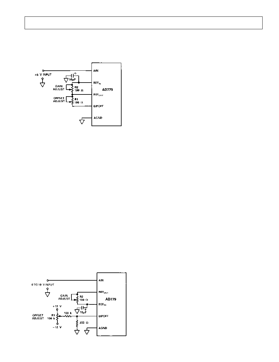
The connections for the bipolar mode are shown in Figure 5. In
this mode, data output coding will be twos complement binary.
This circuit will allow approximately
±
25 mV of offset trim
range (
±
40 LSB) and
±
0.5% of gain trim range (
±
80 LSB).
Figure 5. Bipolar Input Connections with Gain and
Offset Trims
Either or both of the trim pots can be replaced with 50
±
1%
fixed resistors if the AD779 accuracy limits are sufficient for the
application. If the pins are shorted together, the additional offset
and gain errors will be approximately 80 LSB.
To trim bipolar zero to its nominal value, apply a signal 1/2 LSB
below midrange (0.305 mV for a
±
5 V range) and adjust R1
until the major carry transition is located (11 1111 1111 1111 to
00 0000 0000 0000). To trim the gain, apply a signal 1 1/2 LSB
below full scale (+4.9991 V for a
±
5 V range) and adjust R2 to
give the last positive transition (01 1111 1111 1110 to 01 1111
1111 1111). These trims are interactive so several iterations may
be necessary for convergence.
A single pass calibration can be done by substituting a bipolar
offset trim (error at minus full scale) for the bipolar zero trim
(error at midscale), using the same circuit. First, apply a signal
1/2 LSB above minus full scale (4.9997 V for a
±
5 V range)
and adjust R1 until the minus full-scale transition is located
(10 0000 0000 0000 to 10 000 000 0001). Then perform the
gain error trim as outlined above.
UNIPOLAR RANGE INPUTS
Offset and gain errors can be trimmed out by using the configu-
ration shown in Figure 6. This circuit allows approximately
±
25 mV of offset trim range (
±
40 LSB) and
±
0.5% of gain trim
range (
±
80 LSB).
Figure 6. Unipolar Input Connections with Gain and
Offset Trims
The first transition (from 00 0000 0000 0000 to 00 0000 0000
0001) should nominally occur for an input level of +1/2 LSB
(0.305 mV above ground for a 10 V range). To trim unipolar
zero to this nominal value, apply a 0.305 mV signal to AIN and
adjust R1 until the first transition is located.
The gain trim is done by adjusting R2. If the nominal value is
required, apply a signal 1 1/2 LSB below full scale (9.9997 V for
a 10 V range) and adjust R2 until the last transition is located
(11 1111 1111 1110 to 11 1111 1111 1111).
If offset adjustment is not required, BIPOFF should be con-
nected directly to AGND. If gain adjustment is not required, R2
should be replaced with a fixed 50
±
1% metal film resistor. If
REF
OUT
is connected directly to REF
IN
, the additional gain
error will be approximately 1%.
REFERENCE DECOUPLING
It is recommended that a 10
µ
F tantalum capacitor be
connected between REF
IN
(Pin 9) and ground. This has the
effect of improving the S/N+D ratio through filtering possible
broadband noise contributions from the voltage reference.
BOARD LAYOUT
Designing with high resolution data converters requires careful
attention to board layout. Trace impedance is a significant issue.
A 1.22 mA current through a 0.5
trace will develop a voltage
drop of 0.6 mV, which is 1 LSB at the 14-bit level for a 10 V
full-scale span. In addition to ground drops, inductive and
capacitive coupling need to be considered, especially when high
accuracy analog signals share the same board with digital signals.
Finally, power supplies need to be decoupled in order to filter
out ac noise.
Analog and digital signals should not share a common path.
Each signal should have an appropriate analog or digital return
routed close to it. Using this approach, signal loops enclose a
small area, minimizing the inductive coupling of noise. Wide PC
tracks, large gauge wire, and ground planes are highly recom-
mended to provide low impedance signal paths. Separate analog
and digital ground planes are also desirable, with a single
interconnection point to minimize ground loops. Analog signals
should be routed as far as possible from digital signals and
should cross them at right angles.
The AD779 incorporates several features to help the user's layout.
Analog pins (V
BE
) AIN, AGND, REF
OUT
, REF
IN
, BIPOFF,
V
CC
) are adjacent to help isolate analog from digital signals. In
addition, the 10 M
input impedance of AIN minimizes input
trace impedance errors. Finally, ground currents have been
minimized by careful circuit design. Current through AGND is
200
µ
A, with no code dependent variation. The current through
DGND is dominated by the return current for DB13DB0 and
EOC.
SUPPLY DECOUPLING
The AD779 power supplies should be well filtered, well regulated,
and free from high frequency noise. Switching power supplies
are not recommended due to their tendency to generate spikes
which can induce noise in the analog system.
Decoupling capacitors should be used as close as possible to all
power supply pins. A 10
µ
F tantalum capacitor in parallel with a
0.1
µ
F ceramic capacitor provides adequate decoupling.
AD779
10
REV. B
An effort should be made to minimize the trace length between
the capacitor leads and the respective converter power supply
and common pins. The circuit layout should attempt to locate
the AD779, associated analog input circuitry and interconnec-
tions as far as possible from logic circuitry. A solid analog
ground plane around the AD779 will isolate large switching
ground currents. For these reasons, the use of wire wrap circuit
construction is not recommended; careful printed circuit con-
struction is preferred.
GROUNDING
If a single AD779 is used with separate analog and digital
ground planes, connect the analog ground plane to AGND and
the digital ground plane to DGND keeping lead lengths as short
as possible. Then connect AGND and DGND together at the
AD779. If multiple AD779s are used or the AD779 shares
analog supplies with other components, connect the analog and
digital returns together once at the power supplies rather than at
each chip. This prevents large ground loops which inductively
couple noise and allow digital currents to flow through the
analog system.
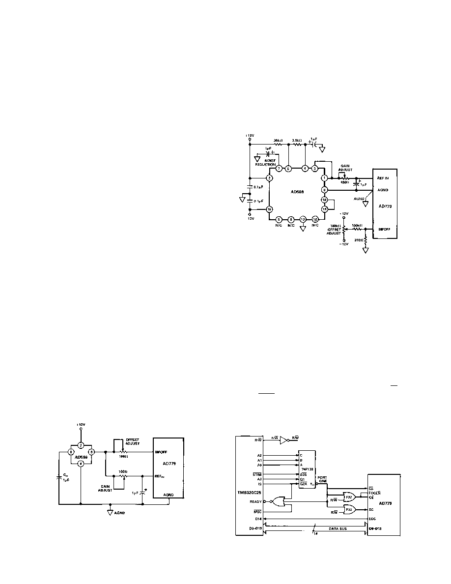
USE OF EXTERNAL VOLTAGE REFERENCE
The AD779 features an on-chip voltage reference. For improved
gain accuracy over temperature, a high performance external
voltage reference may be used in place of the on-chip reference.
The AD586 and AD588 are popular references appropriate for
use with high resolution converters. The AD586 is a low cost
reference which utilizes a buried Zener architecture to provide
low noise and drift. The AD588 is a higher performance refer-
ence which uses a proprietary ion-implanted buried Zener diode
in conjunction with laser-trimmed thin-film resistors for low off-
set and low drift.
Figure 7 shows the use of the AD586 with the AD779 in a bipo-
lar input mode. Over the 0
°
C to +70
°
C range, the AD586 L-grade
exhibits less than a 2.25 mV output change from its initial value
at 25
°
C. REF
IN
, (Pin 9) scales its input by a factor of two; thus,
this change becomes effectively 4.5 mV. When applied to the
AD779, this results in a total gain drift of 0.09% FSR which is
an improvement over the on-chip reference performance of
0.11% FSR. A noise-reduction capacitor, C
N
, has been shown.
This capacitor reduces the broadband noise of the AD586 out-
put, thereby optimizing the overall ac and dc performance of the
AD779.
Figure 7. Bipolar Input with Gain and Offset Trims
Figure 8 shows the AD779 in unipolar input mode with the
AD588 reference. The AD588 output is accurate to 0.65 mV
from its value at 25
°
C over the 0
°
C to 70
°
C range. This results
in a 0.06% FSR total gain drift for the AD779, which is a sub-
stantial improvement over the on-chip reference performance of
0.11% FSR. A noise-reduction network on Pins 4, 6 and 7 has
been shown. The 1
µ
F capacitors form low pass filters with the
internal resistance of the AD588 Zener and amplifier cells and
external resistance. This reduces the high frequency noise of
the AD588, providing optimum ac and dc performance of the
AD779.
Figure 8. Unipolar Input with Gain and Offset Trims
INTERFACING THE AD779 TO MICROPROCESSORS
The I/O capabilities of the AD779 allow direct interfacing to
general purpose and DSP microprocessor buses. The asynchro-
nous conversion control feature allows complete flexibility and
control with minimal external hardware.
The following examples illustrate typical AD779 interface
configurations.
AD779 TO TMS320C25
In Figure 9 the AD779 is mapped into the TMS320C25 I/O
space. AD779 conversions are initiated by issuing an OUT
instruction to Port 1. EOC status and the conversion result are
read in with an IN instruction to Port 1. A single wait state is
inserted by generating the processor READY input from IS,
Port 1 and MSC. This configuration supports processor clock
speeds of 20 MHz and is capable of supporting processor clock
speeds of 40 MHz if a NOP instruction follows each AD779
read instruction.
Figure 9. AD779 to TMS320C25 Interface
AD779
11
REV. B
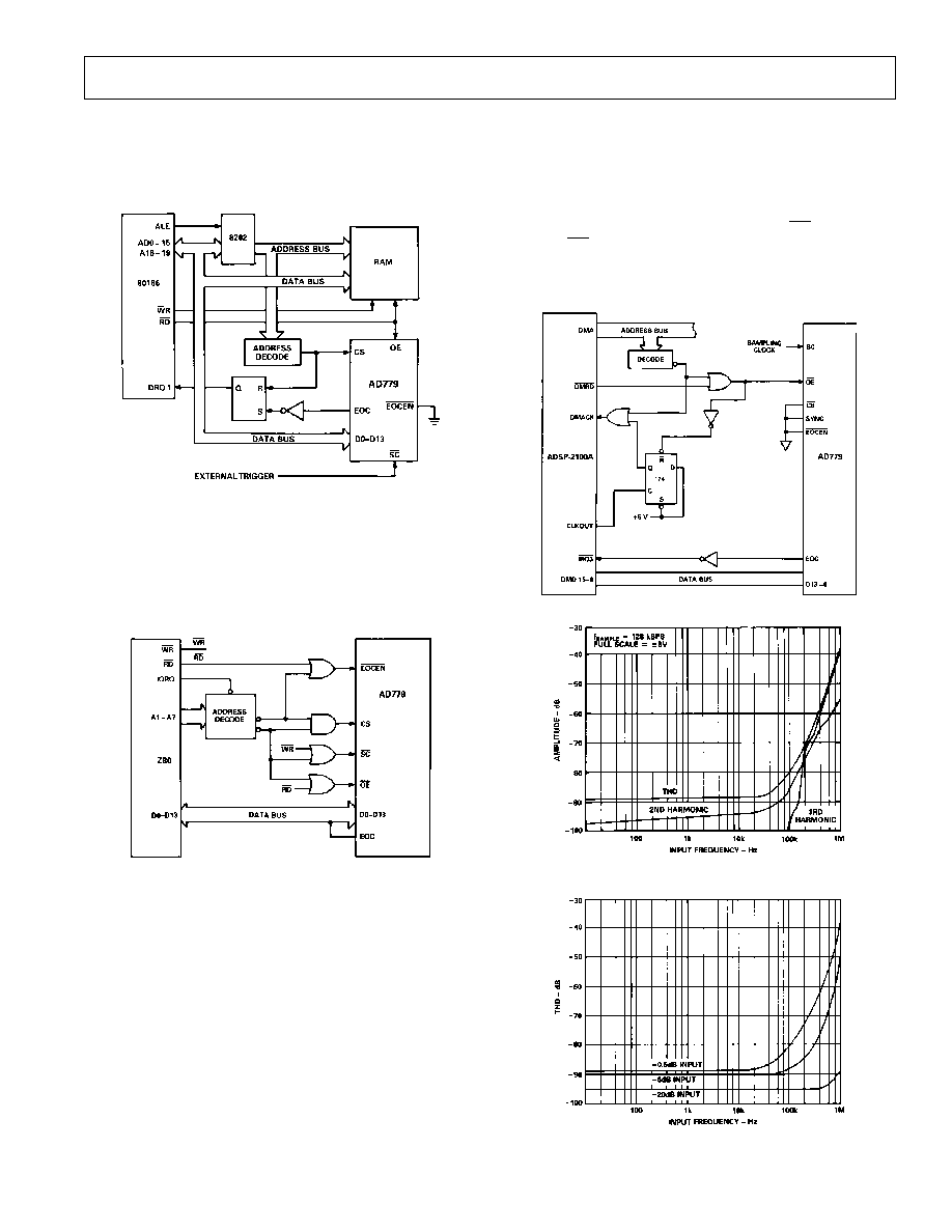
AD779 TO 80186
Figure 10 shows the AD779 interfaced to the 80186 micropro-
cessor. This interface allows the 80186's built-in DMA control-
ler to transfer the AD779 output into a RAM based FIFO buffer
of any length, with no microprocessor intervention.
Figure 10. AD779 to 80186 DMA Interface
AD779 TO Z80
The AD779 can be interfaced to the Z80 processor in an I/O or
memory mapped configuration. Figure 11 illustrates an I/O con-
figuration, where the AD779 occupies several port addresses to
allow separate polling of the EOC status and reading of the data.
Figure 11. AD779 to Z80 Interface
A useful feature of the Z80 is that a single wait state is automati-
cally inserted during I/O operations, allowing the AD779 to be
used with Z80 processors having clock speeds up to 8 MHz.
The AD779 is asynchronous which allows conversions to be ini-
tiated by an external trigger source independent of the micro-
processor clock. After each conversion, the AD779 EOC signal
generates a DMA request to Channel 1 (DRQ1). The subse-
quent DMA READ resets the interrupt latch. The system de-
signer must assign a sufficient priority to the DMA channel to
ensure that the DMA request will be serviced before the com-
pletion of the next conversion. This configuration can be used
with 6 MHz and 8 MHz 80186 processors.
AD779 TO ANALOG DEVICES ADSP-2100A
Figure 12 demonstrates the AD779 interfaced to an ADSP-
2100A. With a clock frequency of 12.5 MHz, and instruction
execution in one 80 ns cycle, the digital signal processor will
support the AD779 data memory interface with two wait states.
The converter runs asychronously using a sampling clock. The
EOC output to the AD779 gets asserted at the end of each
conversion and causes an interrupt. Upon interrupt, the ADSP-
2100A starts a data memory read by providing an address on
the DMA bus. The decoded address generates OE for the
converter. OE, together with logic and latch, is used to force the
ADSP-2100A into a one cycle wait state by generating
DMACK. The read operation is thus started and completed
within two processor cycles (160 ns).
Figure 12. AD779 to ADSP-2100A Interface
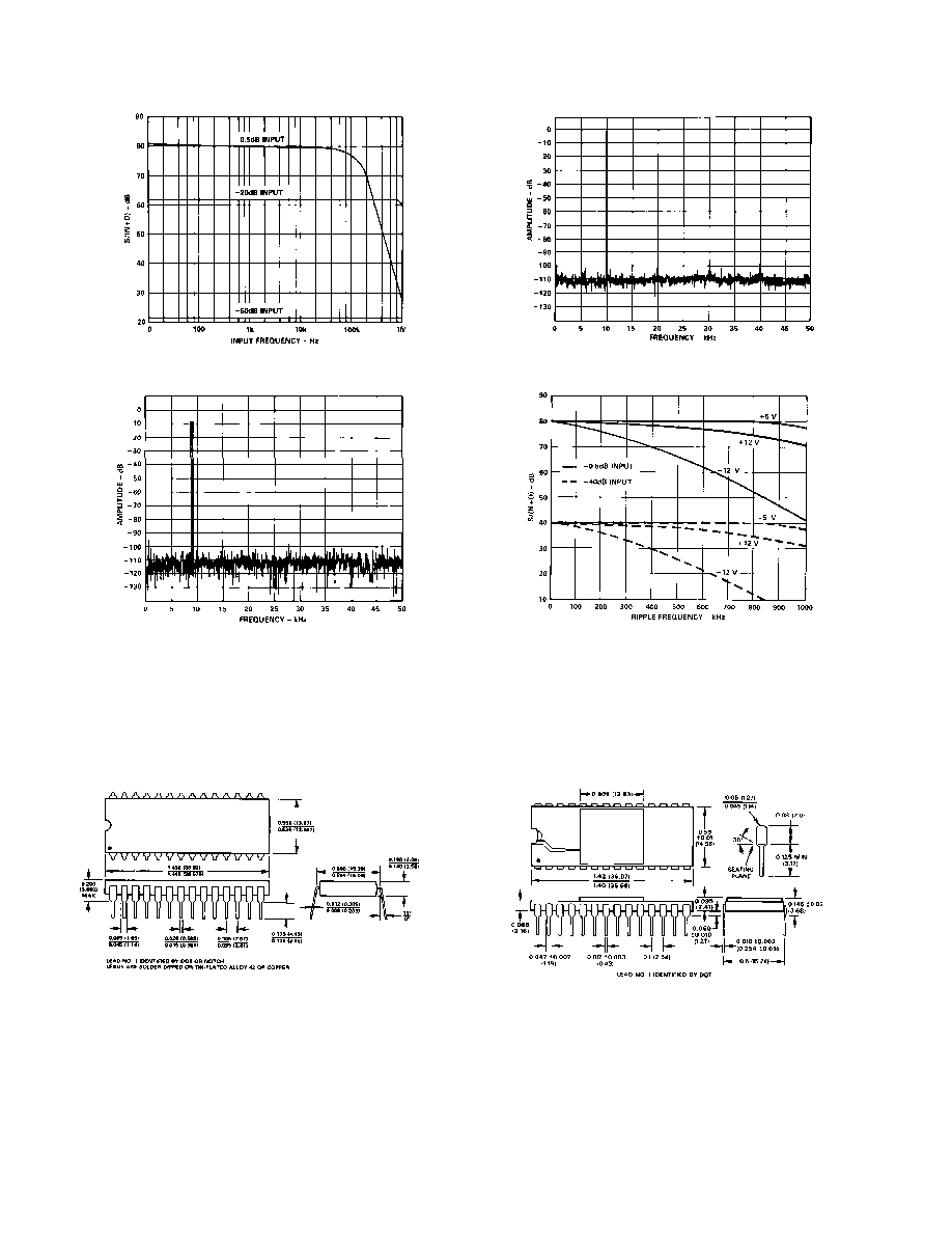
Figure 13. Harmonic Distortion vs. Input Frequency
(0.5 dB Input)
Figure 14. Total Harmonic Distortion vs. Input Frequency
and Amplitude
AD779
12
REV. B
C1438a53/92
PRINTED IN U.S.A.
Figure 15. S/(N+D) vs. Input Frequency and Amplitude
Figure 17. Nonaveraged IMD Plot for f
IN
= 9.08 kHz (f
a
),
9.58 kHz (f
b
) at 128 kSPS
Figure 16. 5-Plot Averaged 2048-Point FFT at 128 kSPS,
f
lN
= 10.009 kHz
Figure 18. Power Supply Rejection (f
IN
= 10 kHz,
f
SAMPLE
= 128 kSPS, V
RIPPLE
= 0.1 V p-p)
OUTLINE DIMENSIONS
Dimensions shown in inches and (mm).
28-Lead Ceramic DIP Package (D-28)
28-Lead Plastic DIP Package (N-28)
Document Outline
- Specifications
- Pinout
- Package drawings
- Ordering Guide
- Features
- Product Description
- Absolute Maximum Ratings
- Functional Block Diagram
- PRODUCT HIGHLIGHTS
- DIGITAL SPECIFICATIONS
- DC SPECIFICATIONS
- TIMING SPECIFICATIONS
- ESD SENSITIVITY
- PIN DESCRIPTION
- DEFINITION OF SPECIFICATIONS
- CONVERSION TRUTH TABLE
- CONVERSION CONTROL
- END-OF-CONVERT
- OUTPUT ENABLE OPERATION
- POWER-UP
- Application Information
- INPUT CONNECTIONS AND CALIBRATION
- BIPOLAR RANGE INPUTS
- UNIPOLAR RANGE INPUTS
- REFERENCE DECOUPLING
- BOARD LAYOUT
- SUPPLY DECOUPLING
- GROUNDING
- USE OF EXTERNAL VOLTAGE REFERENCE
- INTERFACING THE AD779 TO MICROPROCESSORS
- AD779 TO TMS320C25
- AD779 TO 80186
- AD779 TO Z80
- AD779 TO ANALOG DEVICES ADSP-2100A
- OUTLINE DIMENSIONS
- DIAGRAMS
- Conversion Timing
- Output Timing
- EOC Timing
- Load Circuit for Bus Timing Specifications
- Bipolar Input Connections with Gain and
- Unipolar Input Connections with Gain and Offset Trims
- Bipolar Input with Gain and Offset Trims
- Unipolar Input with Gain and Offset Trims
- AD779 to TMS320C25 Interface
- AD779 to 80186 DMA Interface
- AD779 to Z80 Interface
- AD779 to ADSP-2100A Interface
- Harmonic Distortion vs. Input Frequency
- Total Harmonic Distortion vs. Input Frequency and Amplitude
- S/(N+D) vs. Input Frequency and Amplitude
- Plot Averaged 2048-Point FFT at 128 kSPS,
- Nonaveraged IMD Plot for fIN = 9.08 kHz (fa),
- Power Supply Rejection (fIN = 10 kHz,