 | ÐлекÑÑоннÑй компоненÑ: AD7892-3 | СкаÑаÑÑ:  PDF PDF  ZIP ZIP |
/home/web/doc/html/ad/164329
AD7892
a
LC
2
MOS Single Supply,
12-Bit 600 kSPS ADC
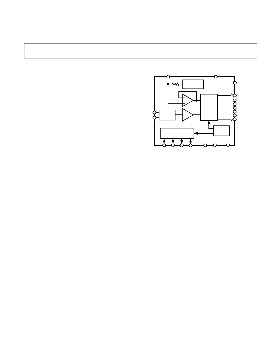
FUNCTIONAL BLOCK DIAGRAM
REF OUT/REF IN
V
DD
+2.5V
REFERENCE
2k
12-BIT
ADC
TRACK/HOLD
SIGNAL
SCALING
AD7892
MODE
DB0
DB2
DB10/LOW
DB11/LOW
DGND
AGND
CONTROL LOGIC
CONVST
EOC
RD
CS
V
IN1
V
IN2
CLOCK
DB3/
RFS
DB4/SCLK
DB5/SDATA
STANDBY
The AD7892 is fabricated in Analog Devices' Linear Compat-
ible CMOS (LC
2
MOS) process, a mixed technology process
that combines precision bipolar circuits with low power CMOS
logic. It is available in a 24-lead, 0.3" wide, plastic or hermetic
DIP or in a 24-lead SOIC.
PRODUCT HIGHLIGHTS
1. The AD7892-3 features a conversion time of 1.47
µs and a
track/hold acquisition time of 200 ns. This allows a through-
put rate for the part up to 600 kSPS. The AD7892-1 and
AD7892-2 operate with throughput rates of 500 kSPS.
2. The AD7892 operates from a single +5 V supply and con-
sumes 60 mW typ making it ideal for low power and portable
applications.
3. The part offers a high speed, flexible interface arrangement
with parallel and serial interfaces for easy connection to
microprocessors, microcontrollers and digital signal
processors.
GENERAL DESCRIPTION
The AD7892 is a high speed, low power, 12-bit A/D converter
that operates from a single +5 V supply. The part contains a
1.47
µs successive approximation ADC, an on-chip track/hold
amplifier, an internal +2.5 V reference and on-chip versatile
interface structures that allow both serial and parallel connec-
tion to a microprocessor. The part accepts an analog input range
of
±10 V or ±5 V (AD7892-1), 0 V to +2.5 V (AD7892-2) and
±2.5 V (AD7892-3). Overvoltage protection on the analog inputs
for the AD7892-1 and AD7892-3 allows the input voltage to go
to
±17 V or ±7 V respectively without damaging the ports.
The AD7892 offers a choice of two data output formats: a
single, parallel, 12-bit word or serial data. Fast bus access times
and standard control inputs ensure easy parallel interface to
microprocessors and digital signal processors. A high speed
serial interface allows direct connection to the serial ports of
microcontrollers and digital signal processors.
In addition to the traditional dc accuracy specifications such as
linearity, full-scale and offset errors, the part is also specified for
dynamic performance parameters including harmonic distortion
and signal-to-noise ratio.
REV. C
Information furnished by Analog Devices is believed to be accurate and
reliable. However, no responsibility is assumed by Analog Devices for its
use, nor for any infringements of patents or other rights of third parties
which may result from its use. No license is granted by implication or
otherwise under any patent or patent rights of Analog Devices.
FEATURES
Fast 12-Bit ADC with 1.47
s Conversion Time
600 kSPS Throughput Rate (AD7892-3)
500 kSPS Throughput Rate (AD7892-1, AD7892-2)
Single Supply Operation
On-Chip Track/Hold Amplifier
Selection of Input Ranges:
10 V or 5 V for AD7892-1
0 V to +2.5 V for AD7892-2
2.5 V for AD7892-3
High Speed Serial and Parallel Interface
Low Power, 60 mW typ
Overvoltage Protection on Analog Inputs (AD7892-1
and AD7892-3)
One Technology Way, P.O. Box 9106, Norwood, MA 02062-9106, U.S.A.
Tel: 781/329-4700
World Wide Web Site: http://www.analog.com
Fax: 781/326-8703
© Analog Devices, Inc., 2000

(V
DD
= +5 V 5%, AGND = DGND = 0 V, REF IN = +2.5 V. All specifications T
MIN
to T
MAX
unless otherwise noted.)
AD7892SPECIFICATIONS
Parameter
A Versions
1
B Versions
S Version
2
Unit
Test Conditions/Comments
DYNAMIC PERFORMANCE
AD7892-1, AD7892-2
f
IN
= 100 kHz. f
SAMPLE
= 500 kSPS
Signal to (Noise + Distortion) Ratio
3
70
70
70
dB min
Total Harmonic Distortion
3
78
78
78
dB max
typ 84 dB
Peak Harmonic or Spurious Noise
3
79
79
79
dB max
Intermodulation Distortion
3
fa = 49 kHz, fb = 50 kHz
2nd Order Terms
78
78
78
dB max
typ 84 dB
3rd Order Terms
78
78
78
dB max
typ 84 dB
AD7892-3
f
IN
= 100 kHz. f
SAMPLE
= 600 kSPS
Signal to (Noise + Distortion) Ratio
3
70
70
dB min
Total Harmonic Distortion
3
78
78
dB max
Peak Harmonic or Spurious Noise
3
79
79
dB max
Intermodulation Distortion
3
fa = 49 kHz, fb = 50 kHz
2nd Order Terms
78
78
dB max
3rd Order Terms
78
78
dB max
DC ACCURACY
Resolution
12
12
12
Bits
Minimum Resolution for Which No
Missing Codes Are Guaranteed
12
12
12
Bits
Relative Accuracy
3
±1.5
±1
±1
LSB max
Differential Nonlinearity
3
±1
±1
±1
LSB max
AD7892-1
Positive Full-Scale Error
3
±4
±4
±5
LSB max
Negative Full-Scale Error
3
±4
±4
±5
LSB max
Bipolar Zero Error
3
±3
±2
±3
LSB max
AD7892-3
Positive Full-Scale Error
3
±4
±4
LSB max
Negative Full-Scale Error
3
±4
±4
LSB max
Bipolar Zero Error
3
±4
±3
LSB max
AD7892-2
Positive Full-Scale Error
3
±5
±5
±5
LSB max
Unipolar Offset Error
3
±4
±3
±4
LSB max
ANALOG INPUT
AD7892-1
Input Voltage Range
±10
±10
±10
Volts
Input Applied to V
IN1
with V
IN2
Grounded
Input Voltage Range
±5
±5
±5
Volts
Input Applied to V
IN1
and V
IN2
Input Resistance
8
8
8
k
min
Input Applied to V
IN1
with V
IN2
Grounded
AD7892-2
Input Voltage Range on V
IN1
0 to +2.5
0 to +2.5
0 to +2.5
Volts
Input Applied to V
IN1
Input Current
10
10
50
nA max
Input Voltage Range on V
IN2
±50
±50
±50
mV max
AD7892-3
Input Voltage Range on V
IN1
±2.5
±2.5
Volts
Input Applied to V
IN1
Input Resistance
2
2
k
min
REFERENCE OUTPUT/INPUT
REF IN Input Voltage Range
2.375/2.625
2.375/2.625
2.375/2.625
V min/V max
2.5 V
± 5%
Input Impedance
1.6
1.6
1.6
k
min
Resistor Connected to Internal Reference Node
Input Capacitance
4
10
10
10
pF max
REF OUT Output Voltage
2.5
2.5
2.5
V nom
REF OUT Error @ +25
°C
±10
±10
±10
mV max
T
MIN
to T
MAX
±20
±20
±25
mV max
REF OUT Temperature Coefficient
25
25
25
ppm/
°C typ
REF OUT Output Impedance
5.5
5.5
5.5
k
nom
LOGIC INPUTS
Input High Voltage, V
INH
2.4
2.4
2.4
V min
V
DD
= 5 V
± 5%
Input Low Voltage, V
INL
0.8
0.8
0.8
V max
V
DD
= 5 V
± 5%
Input Current, I
IN
±10
±10
±10
µA max
V
IN
= 0 V to V
DD
Input Capacitance, C
IN
4
10
10
10
pF max
2
REV. C

ABSOLUTE MAXIMUM RATINGS*
(T
A
= +25
°C unless otherwise noted)
V
DD
to AGND . . . . . . . . . . . . . . . . . . . . . . . . . 0.3 V to +7 V
V
DD
to DGND . . . . . . . . . . . . . . . . . . . . . . . . . 0.3 V to +7 V
Analog Input Voltage to AGND
AD7892-1 . . . . . . . . . . . . . . . . . . . . . . . . . . . . . . . . .
±17 V
AD7892-2 . . . . . . . . . . . . . . . . . . . . . . . . . . . . 0.3 V, V
DD
AD7892-3 . . . . . . . . . . . . . . . . . . . . . . . . . . . . . . . . . .
±7 V
Reference Input Voltage to AGND . . . 0.3 V to V
DD
+ 0.3 V
Digital Input Voltage to DGND . . . . . 0.3 V to V
DD
+ 0.3 V
Digital Output Voltage to DGND . . . . 0.3 V to V
DD
+ 0.3 V
Operating Temperature Range
Commercial (A, B Versions) . . . . . . . . . . . 40
°C to +85°C
Extended (S Version) . . . . . . . . . . . . . . . . 55
°C to +125°C
Storage Temperature Range . . . . . . . . . . . . 65
°C to +150°C
Parameter
A Versions
1
B Versions
S Version
2
Unit
Test Conditions/Comments
LOGIC OUTPUTS
Output High Voltage, V
OH
4.0
4.0
4.0
V min
I
SOURCE
= 200
µA
Output Low Voltage, V
OL
0.4
0.4
0.4
V max
I
SINK
= 1.6 mA
DB11DB0
Floating-State Leakage Current
±10
±10
±10
µA max
Floating-State Capacitance
4
15
15
15
pF max
Output Coding
AD7892-1 and AD7892-3
Two's Complement
AD7892-2
Straight (Natural) Binary
CONVERSION RATE
Conversion Time
1.47
1.47
µs max
AD7892-3
Track/Hold Acquisition Time
3
0.2
0.2
µs max
AD7892-3
Conversion Time
1.6
1.6
1.68
µs max
AD7892-1 and AD7892-2
Track/Hold Acquisition Time
3
0.4
0.4
0.32
µs max
AD7892-1 and AD7892-2
POWER REQUIREMENTS
V
DD
+5
+5
+5
V nom
±5% for Specified Performance
I
DD
5
Normal Operation
18
18
19
mA max
Standby Mode
6
AD7892-2
250
250
µA typ
AD7892-3, AD7892-1
80
80
100
µA max
typ 15
µA
Power Dissipation
5
Normal Operation
90
90
95
mW max
V
DD
= +5 V. Typically 60 mW
Standby Mode
6
AD7892-2
1.25
1.25
mW typ
AD7892-3, AD7892-1
400
400
500
µW max
V
DD
= +5 V. Typically 75
µW
NOTES
1
Temperature ranges are as follows: A, B Versions: 40
°C to +85°C; S Version: 55°C to +125°C.
2
S Version available on AD7892-1 and AD7892-2 only.
3
See Terminology.
4
Sample tested @ +25
°C to ensure compliance.
5
These normal mode and standby mode currents are achieved with resistors (in the range 10 k
to 100 k) to either DGND or V
DD
on Pins 8, 9, 16 and 17.
6
A conversion should not be initiated on the part within 30
µs of exiting standby mode.
Specifications subject to change without notice.
AD7892
Junction Temperature . . . . . . . . . . . . . . . . . . . . . . . . . +150
°C
Plastic DIP Package, Power Dissipation . . . . . . . . . . 450 mW
JA
Thermal Impedance . . . . . . . . . . . . . . . . . . . . . 105
°C/W
Lead Temperature (Soldering, 10 sec) . . . . . . . . . . . +260
°C
Cerdip Package, Power Dissipation . . . . . . . . . . . . . . 450 mW
JA
Thermal Impedance . . . . . . . . . . . . . . . . . . . . . . 70
°C/W
Lead Temperature (Soldering, 10 sec) . . . . . . . . . . . +300
°C
SOIC Package, Power Dissipation . . . . . . . . . . . . . . . 450 mW
JA
Thermal Impedance . . . . . . . . . . . . . . . . . . . . . . 75
°C/W
Lead Temperature, Soldering
Vapor Phase (60 sec) . . . . . . . . . . . . . . . . . . . . . . +215
°C
Infrared (15 sec) . . . . . . . . . . . . . . . . . . . . . . . . . . +220
°C
*Stresses above those listed under Absolute Maximum Ratings may cause perma-
nent damage to the device. This is a stress rating only; functional operation of the
device at these or any other conditions above those listed in the operational
sections of this specification is not implied. Exposure to absolute maximum rating
conditions for extended periods may affect device reliability.
REV. C
3
AD7892
4
REV. C
TIMING CHARACTERISTICS
1, 2
A, B
S
Parameter
Versions
Version
Unit
Test Conditions/Comments
t
CONV
1.47
µs max
Conversion Time for AD7892-3
1.6
1.68
µs max
Conversion Time for AD7892-1, AD7892-2
t
ACQ
200
ns min
Acquisition Time for AD7892-3
400
320
ns min
Acquisition Time for AD7892-1, AD7892-2
Parallel Interface
t
1
35
45
ns min
CONVST Pulsewidth
t
2
60
60
ns min
EOC Pulsewidth
t
3
0
0
ns min
EOC Falling Edge to CS Falling Edge Setup Time
t
4
0
0
ns min
CS to RD Setup Time
t
5
35
45
ns min
Read Pulsewidth
t
6
3
35
40
ns max
Data Access Time After Falling Edge of
RD
t
7
4
5
5
ns min
Bus Relinquish Time After Rising Edge of
RD
30
40
ns max
t
8
0
0
ns min
CS to RD Hold Time
t
9
200
200
ns min
RD to CONVST Setup Time
Serial Interface
t
10
30
35
ns min
RFS Low to SCLK Falling Edge Setup Time
t
11
3
25
30
ns max
RFS Low to Data Valid Delay
t
12
25
25
ns min
SCLK High Pulsewidth
t
13
25
25
ns min
SCLK Low Pulsewidth
t
14
3
5
5
ns min
SCLK Rising Edge to Data Valid Hold Time
t
15
3
25
30
ns max
SCLK Rising Edge to Data Valid Delay
t
16
20
30
ns min
RFS to SCLK Falling Edge Hold Time
t
17
4
0
0
ns min
Bus Relinquish Time after Rising Edge of
RFS
30
30
ns max
t
17A
4
0
0
ns min
Bus Relinquish Time after Rising Edge of SCLK
30
30
ns max
NOTES
1
Sample tested at +25
°C to ensure compliance. All input signals are measured with tr = tf = 1 ns (10% to 90% of +5 V) and timed from a voltage level of +1.6 V.
2
See Figures 2 and 3.
3
Measured with the load circuit of Figure 1 and defined as the time required for an output to cross 0.8 V or 2.4 V.
4
These times are derived from the measured time taken by the data outputs to change 0.5 V when loaded with the circuit of Figure 1. The measured number is then
extrapolated back to remove the effects of charging or discharging the 50 pF capacitor. This means that the times quoted in the timing characteristics are the true bus
relinquish times of the part and as such are independent of external bus loading capacitances.
5
Assumes CMOS loads on the data bits. With TTL loads, more current is drawn from the data lines and the
RD to CONVST time needs to be extended to 400 ns min.
Specifications subject to change without notice.
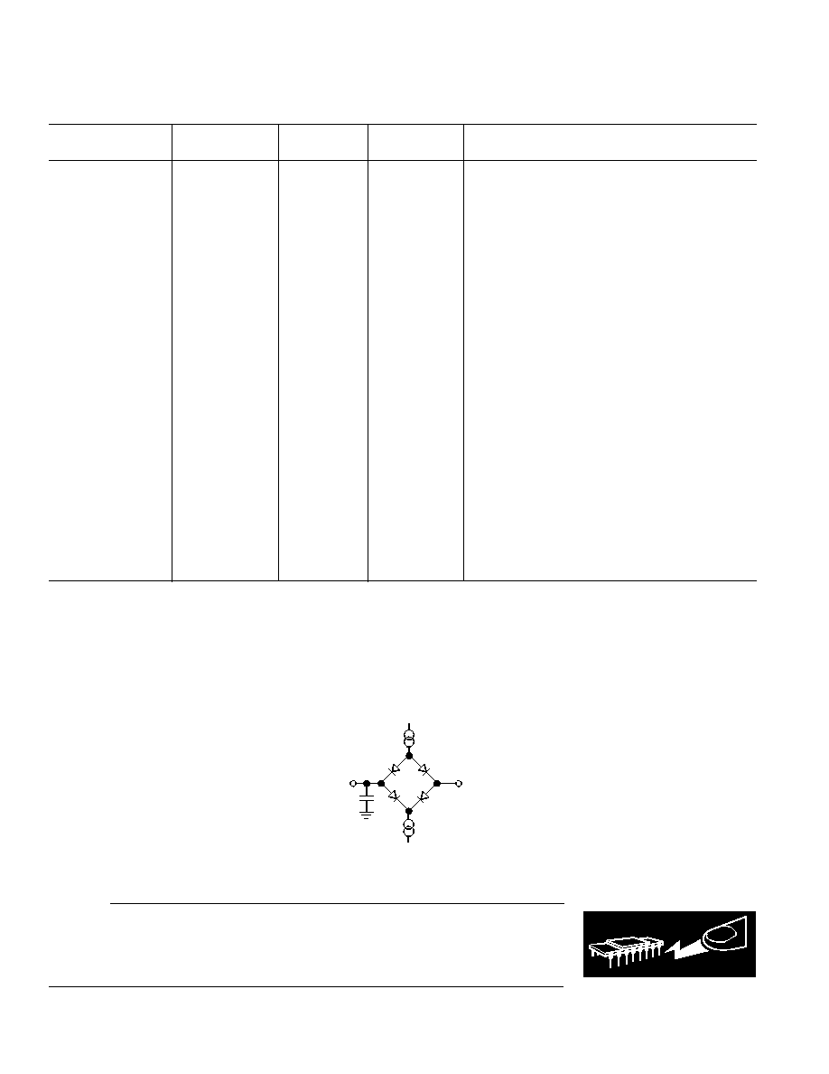
1.6mA
+1.6V
200 A
50pF
TO
OUTPUT
PIN
Figure 1. Load Circuit for Access Time and Bus Relinquish Time
CAUTION
ESD (electrostatic discharge) sensitive device. Electrostatic charges as high as 4000 V readily
accumulate on the human body and test equipment and can discharge without detection.
Although the AD7892 features proprietary ESD protection circuitry, permanent damage may
occur on devices subjected to high energy electrostatic discharges. Therefore, proper ESD
precautions are recommended to avoid performance degradation or loss of functionality.
(V
DD
= +5 V 5%, AGND = DGND = 0 V, REF IN = +2.5 V)
WARNING!
ESD SENSITIVE DEVICE
AD7892
REV. C
5
ORDERING GUIDE
Input
Sample
Relative
Temperature
Package
Model
Range
Rate
Accuracy
Range
Option
1
AD7892AN-1
±5 V or ±10 V
500 kSPS
40
°C to +85°C
N-24
AD7892BN-1
±5 V or ±10 V
500 kSPS
±1 LSB
40
°C to +85°C
N-24
AD7892AR-1
±5 V or ±10 V
500 kSPS
40
°C to +85°C
R-24
AD7892BR-1
±5 V or ±10 V
500 kSPS
±1 LSB
40
°C to +85°C
R-24
AD7892SQ-1
±5 V or ±10 V
500 kSPS
±1 LSB
55
°C to +125°C
Q-24
AD7892AN-2
0 V to +2.5 V
500 kSPS
40
°C to +85°C
N-24
AD7892BN-2
0 V to +2.5 V
500 kSPS
±1 LSB
40
°C to +85°C
N-24
AD7892AR-2
0 V to +2.5 V
500 kSPS
40
°C to +85°C
R-24
AD7892BR-2
0 V to +2.5 V
500 kSPS
±1 LSB
40
°C to +85°C
R-24
AD7892AN-3
±2.5 V
600 kSPS
40
°C to +85°C
N-24
AD7892BN-3
±2.5 V
600 kSPS
±1 LSB
40
°C to +85°C
N-24
AD7892AR-3
±2.5 V
600 kSPS
40
°C to +85°C
R-24
AD7892BR-3
±2.5 V
600 kSPS
±1 LSB
40
°C to +85°C
R-24
EVAL-AD7892-2CB
2
Evaluation Board
EVAL-AD7892-3CB
2
Evaluation Board
EVAL-CONTROL BOARD
3
Controller Board
NOTES
1
N = Plastic DIP; Q = Cerdip; R = SOIC.
2
These boards can be used as stand-alone evaluation boards or in conjunction with the EVAL-CONTROL BOARD for evaluation/demonstration purposes.
3
This board is a complete unit allowing a PC to control and communicate with all Analog Devices' evaluation boards ending in the CB designators.