 | ÐлекÑÑоннÑй компоненÑ: AD7896 | СкаÑаÑÑ:  PDF PDF  ZIP ZIP |
Äîêóìåíòàöèÿ è îïèñàíèÿ www.docs.chipfind.ru
REV. B
Information furnished by Analog Devices is believed to be accurate and
reliable. However, no responsibility is assumed by Analog Devices for its
use, nor for any infringements of patents or other rights of third parties
which may result from its use. No license is granted by implication or
otherwise under any patent or patent rights of Analog Devices.
a
AD7896*
2.7 V to 5.5 V, 12-Bit, 8 s
ADC in 8-Pin SO/DIP
GENERAL DESCRIPTION
The AD7896 is a fast, 12-bit ADC which operates from a single
+2.7 V to 5.5 V supply and is housed in a small 8-pin mini-DIP
and 8-pin SOIC. The part contains an 8
µ
s successive approxi-
mation A/D converter, an on-chip track/hold amplifier, an on-
chip clock and a high speed serial interface.
Output data from the AD7896 is provided via a high speed,
serial interface port. This two-wire serial interface has a serial
clock input and a serial data output with the external serial clock
accessing the serial data from the part.
In addition to the traditional dc accuracy specifications such as
linearity, full-scale and offset errors, the AD7896 is also speci-
fied for dynamic performance parameters including harmonic
distortion and signal-to-noise ratio.
The part accepts an analog input range of 0 V to V
DD
and oper-
ates from a single +2.7 V to +5.5 V supply consuming only
9 mW typical. The V
DD
input is also used as the reference for
the part so that no external reference is required.
The AD7896 features a high sampling rate mode and, for low
power applications, a proprietary automatic power down mode
where the part automatically goes into power down once con-
version is complete and "wakes up" before the next conversion
cycle.
The part is available in a small, 8-pin, 0.3'' wide, plastic or her-
metic dual-in-line package (mini-DIP) and in an 8-pin, small
outline IC (SOIC).
*Patent pending.
PRODUCT HIGHLIGHTS
1. Complete, 12-bit ADC in 8-Pin Package
The AD7896 contains an 8
µ
s ADC, a track/hold amplifier,
control logic and a high speed serial interface, all in an 8-pin
DIP. The V
DD
input is used as the reference for the part so
no external reference is needed. This offers considerable
space saving over alternative solutions.
2. Low Power, Single Supply Operation
The AD7896 operates from a single +2.7 V to 5.5 V supply
and consumes only 9 mW typical. The automatic power
down mode, where the part goes into power down once con-
version is complete and "wakes up" before the next conver-
sion cycle, makes the AD7896 ideal for battery powered or
portable applications.
3. High Speed Serial Interface
The part provides high speed serial data and serial clock lines
allowing for an easy, two-wire serial interface arrangement.
FEATURES
100 kHz Throughput Rate
Fast 12-Bit Sampling ADC with 8 s Conversion Time
8-Pin Mini-DIP and SOIC
Single +2.7 V to +5.5 V Supply Operation
High Speed, Easy-to-Use, Serial Interface
On-Chip Track/Hold Amplifier
Analog Input Range is 0 V to Supply
High Input Impedance
Low Power: 9 mW typ
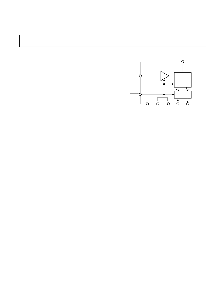
FUNCTIONAL BLOCK DIAGRAM
CLOCK
12-BIT
ADC
OUTPUT
REGISTER
TRACK/HOLD
AD7896
V
I N
CONVST
V
DD
AGND
DGND
BUSY
SCLK
SDATA
© Analog Devices, Inc., 1996
One Technology Way, P.O. Box 9106, Norwood, MA 02062-9106, U.S.A.
Tel: 617/329-4700
Fax: 617/326-8703

A
B
J
S
Parameter
Versions
1
Versions
Version
Version
Units
Test Conditions/Comments
DYNAMIC PERFORMANCE
2
Signal to (Noise + Distortion) Ratio
3
@ +25
°
C
70
70
70 typ
70
dB min
f
IN
=10 kHz Sine Wave, f
SAMPLE
= 100 kHz
T
MIN
to T
MAX
70
dB min
Total Harmonic Distortion (THD)
3
80
80
80 typ
80
dB max
f
IN
= 10 kHz Sine Wave, f
SAMPLE
= 100 kHz
Peak Harmonic or Spurious Noise
3
80
80
80 typ
dB max
f
IN
= 10 kHz Sine Wave, f
SAMPLE
= 100 kHz
Intermodulation Distortion (IMD)
3
fa = 9 kHz, fb = 9.5 kHz, f
SAMPLE
= 100 kHz
2nd Order Terms
80
80
80 typ
80
dB max
3rd Order Terms
80
80
80 typ
80
dB max
DC ACCURACY
Resolution
12
12
12
12
Bits
Minimum Resolution for which No
Missing Codes are Guaranteed
12
12
12
12
Bits
Relative Accuracy
3
±
1
±
1/2
±
1
±
1
LSB max
Differential Nonlinearity
3
±
1
±
1
±
1
±
1
LSB max
Positive Full-Scale Error
3
±
3
±
1.5
±
3
±
3
LSB max
Unipolar Offset Error
±
4
±
4
±
5
±
4
LSB max
V
DD
= 5 V
±
10%
±
4
±
3
±
5
±
4
LSB max
V
DD
= 2.7 V to 3.6 V
ANALOG INPUT
Input Voltage Range
0 to +V
DD
0 to +V
DD
0 to +V
DD
0 to +V
DD
Volts
Input Current
±
2
±
2
±
2
±
5
µ
A max
LOGIC INPUTS
Input High Voltage, V
INH
2.0
2.0
2.0
2.0
V min
V
DD
= 2.7 V to 3.6 V
2.4
2.4
2.4
2.4
V
DD
= 5 V
±
10%
Input Low Voltage, V
INL
0.8
0.8
0.8
0.8
V max
Input Current, I
IN
±
10
±
10
±
10
±
10
µ
A max
V
IN
= 0 V to V
DD
Input Capacitance, C
IN
4
10
10
10
10
pF max
LOGIC OUTPUTS
Output High Voltage, V
OH
2.4
2.4
2.4
2.4
V min
I
SOURCE
= 2 mA
Output Low Voltage, V
OL
0.4
0.4
0.4
0.4
V max
I
SINK
= 2 mA
Output Coding
Straight (Natural) Binary
CONVERSION RATE
Conversion Time:
Mode 1 Operation
8
8
8
8.5
µ
s max
Mode 2 Operation
5
14
14
14
14.5
µ
s max
Track/Hold Acquisition Time
3
1.5
1.5
1.5
1.5
µ
s max
POWER REQUIREMENTS
V
DD
+2.7/+5.5 +2.7/+5.5 +2.7/+5.5 +2.7/+5.5 V min/max
I
DD
4
4
4
4
mA max
Digital Input @ DGND, V
DD
= 2.7 V to
3.6 V
5
5
5
5
mA max
Digital Inputs @ DGND, V
DD
= 5 V
±
10%
Power Dissipation
10.8
10.8
10.8
10.8
mW max
V
DD
= 2.7 V, Typically 9 mW
Power-Down Mode
Digital Inputs @ DGND
I
DD
@ +25
°
C
5
5
5
µ
A typ
5
µ
A max
V
DD
= 2.7 V to 3.6 V
T
MIN
to T
MAX
15
15
75
75
µ
A max
V
DD
= 2.7 V to 3.6 V
I
DD
@ +25
°
C
50
50
50
50
µ
A max
V
DD
= 5 V
±
10%
T
MIN
to T
MAX
150
150
500
500
µ
A max
V
DD
= 5 V
±
10%
Power Dissipation @ +25
°
C
13.5
13.5
13.5
13.5
µ
W max
V
DD
= 2.7 V
NOTES
1
Temperature ranges are as follows: A, B Versions: 40
°
C to +85
°
C; J Version: 0
°
C to +70
°
C; S Version: 55
°
C to +125
°
C.
2
Applies to Mode 1 operation. See section on operating modes.
3
See Terminology.
4
Sample tested @ +25
°
C to ensure compliance.
5
This 14
µ
s includes the "wake-up" time from standby. This "wake-up" time is timed from the rising edge of CONVST, whereas conversion is timed from the
falling edge of CONVST, for narrow CONVST pulse width the conversion time is effectively the "wake-up" time plus conversion time hence 14
µ
s. This can be
seen from Figure 3. Note that if the CONVST pulse width is greater than 6
µ
s then the effective conversion time will increase beyond 14
µ
s.
Specifications subject to change without notice.
REV. B
2
(V
DD
=
+2.7 V to +5.5 V, AGND = DGND = 0 V. All specifications T
MIN
to T
MAX
unless otherwise noted)
AD7896SPECIFICATIONS
AD7896
REV. B
3
A, B
J
S
Parameter
Versions
Version
Version
Units
Test Conditions/Comments
t
1
40
40
40
ns min
CONVST
Pulse Width
t
2
40
2
40
2
45
2
ns min
SCLK High Pulse Width
t
3
40
2
40
2
45
2
ns min
SCLK Low Pulse Width
t
4
Data Access Time After Falling Edge of SCLK
60
3
60
3
70
3
ns max
V
DD
= 5 V
±
10%
100
3
100
3
110
3
ns max
V
DD
= 2.7 V to +3.6 V
t
5
10
10
10
ns min
Data Hold Time After Falling Edge of SCLK
t
6
50
4
50
4
50
4
ns max
Bus Relinquish Time After Falling Edge of SCLK
NOTES
1
Sample tested at +25
°
C to ensure compliance. All input signals are measured with tr = tf = 1 ns (10% to 90% of V
DD
) and timed from a voltage level of +1.4 V.
2
The SCLK maximum frequency is 10 MHz. Care must be taken when interfacing to account for the data access time, t
4
, and the setup time required for the user's
processor. These two times will determine the maximum SCLK frequency that the user's system can operate with. See Serial Interface section for more information.
3
Measured with the load circuit of Figure 1 and defined as the time required for an output to cross 0.8 V or 2.0 V.
4
Derived from the measured time taken by the data outputs to change 0.5 V when loaded with the circuit of Figure 1. The measured number is then extrapolated back
to remove the effects of charging or discharging the 50 pF capacitor. This means that the time, t
6
, quoted in the timing characteristics is the true bus relinquish time
of the part and as such is independent of external bus loading capacitances.
TIMING CHARACTERISTICS
1
(V
DD
= +2.7 V to +5.5 V, AGND = DGND = 0 V)
ABSOLUTE MAXIMUM RATINGS*
(T
A
= +25
°
C unless otherwise noted)
V
DD
to AGND . . . . . . . . . . . . . . . . . . . . . . . . . . 0.3 V to +7 V
V
DD
to DGND. . . . . . . . . . . . . . . . . . . . . . . . . . 0.3 V to +7 V
Analog Input Voltage to AGND . . . . . . 0.3 V to V
DD
+ 0.3 V
Digital Input Voltage to DGND . . . . . . 0.3 V to V
DD
+ 0.3 V
Digital Output Voltage to DGND . . . . . 0.3 V to V
DD
+ 0.3 V
Operating Temperature Range
Commercial (J Version) . . . . . . . . . . . . . . . . . 0
°
C to +70
°
C
Industrial (A, B Versions) . . . . . . . . . . . . . . . 40
°
C to +85
°
C
Extended (S Version) . . . . . . . . . . . . . . . . . 55
°
C to +125
°
C
Storage Temperature Range . . . . . . . . . . . . . 65
°
C to +150
°
C
Junction Temperature . . . . . . . . . . . . . . . . . . . . . . . . . +150
°
C
Plastic DIP Package, Power Dissipation . . . . . . . . . . . 450 mW
JA
Thermal Impedance . . . . . . . . . . . . . . . . . . . . . 125
°
C/W
JC
Thermal Impedance. . . . . . . . . . . . . . . . . . . . . . 50
°
C/W
Lead Temperature (Soldering, 10 sec) . . . . . . . . . . . +260
°
C
SOIC Package, Power Dissipation . . . . . . . . . . . . . . . . 450 mW
JA
Thermal Impedance . . . . . . . . . . . . . . . . . . . . . 160
°
C/W
JC
Thermal Impedance . . . . . . . . . . . . . . . . . . . . . . 75
°
C/W
Lead Temperature, Soldering
Vapor Phase (60 sec) . . . . . . . . . . . . . . . . . . . . . . +215
°
C
Infrared (15 sec) . . . . . . . . . . . . . . . . . . . . . . . . . . +220
°
C
ESD . . . . . . . . . . . . . . . . . . . . . . . . . . . . . . . . . . . . . . . >4000 V
*Stresses above those listed under "Absolute Maximum Ratings" may cause
permanent damage to the device. This is a stress rating only and functional
operation of the device at these or any other conditions above those listed in the
operational sections of this specification is not implied. Exposure to absolute
maximum rating conditions for extended periods may affect device reliability.
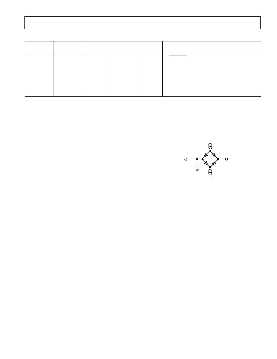
+1.6V
2.0mA
2.0mA
50pF
TO
OUTPUT
PIN
Figure 1. Load Circuit for Access Time and Bus Relinquish
Time
REV. B
4
AD7896
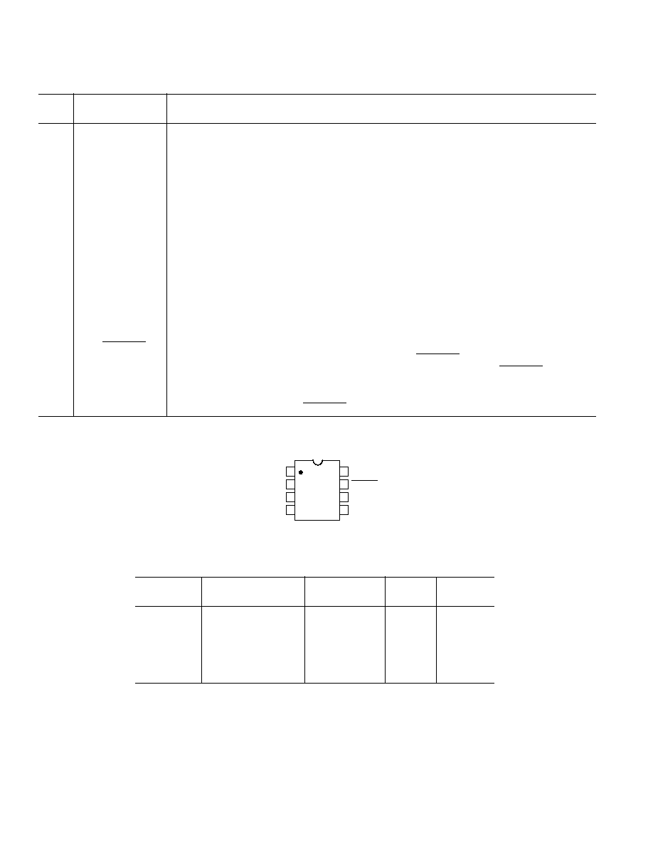
PIN FUNCTION DESCRIPTION
Pin
Pin
No.
Mnemonic
Description
1
V
IN
Analog Input. The analog input range is 0 V to V
DD
.
2
V
DD
Positive supply voltage, +2.7 V to 5.5 V.
3
AGND
Analog Ground. Ground reference for track/hold, comparator and DAC.
4
SCLK
Serial Clock Input. An external serial clock is applied to this input to obtain serial data from
the AD7896. A new serial data bit is clocked out on the falling edge of this serial clock. Data
is guaranteed valid for 10 ns after this falling edge so data can be accepted on the falling edge
when a fast serial clock is used. The serial clock input should be taken low at the end of the
serial data transmission.
5
SDATA
Serial Data Output. Serial data from the AD7896 is provided at this output. The serial data
is clocked out by the falling edge of SCLK, but the data can also be read on the falling edge
of the SCLK. This is possible because data bit N is valid for a specified time after the falling
edge of the SCLK (data hold time) and can be read before data bit N+1 becomes valid a
specified time after the falling edge of SCLK (data access time) (see Figure 4). Sixteen bits
of serial data are provided with four leading zeros followed by the 12 bits of conversion data.
On the sixteenth falling edge of SCLK, the SDATA line is held for the data hold time and
then disabled (three-stated). Output data coding is straight binary.
6
DGND
Digital Ground. Ground reference for digital circuitry.
7
CONVST
Convert Start. Edge-triggered logic input. On the falling edge of this input, the track/hold
goes into its hold mode and conversion is initiated. If CONVST is low at the end of conver-
sion, the part goes into power down mode. In this case, the rising edge of CONVST
"wakes up" the part.
8
BUSY
The BUSY pin is used to indicate when the part is doing a conversion. The BUSY pin will go
high on the falling edge of CONVST and will return low when the conversion is complete.
PIN CONFIGURATION
1
2
3
4
8
7
6
5
TOP VIEW
(Not to Scale)
AD7896
V
I N
SDATA
DGND
CONVST
BUSY
V
DD
AGND
SCLK
ORDERING GUIDE
Temperature
Linearity
SNR
Package
Model
Range
Error (LSB)
(dB)
Option*
AD7896AN
40
°
C to +85
°
C
±
1 LSB
70 dB
N-8
AD7896BN
40
°
C to +85
°
C
±
1/2 LSB
70 dB
N-8
AD7896AR
40
°
C to +85
°
C
±
1 LSB
70 dB
SO-8
AD7896BR
40
°
C to +85
°
C
±
1/2 LSB
70 dB
SO-8
AD7896JR
0
°
C to +70
°
C
±
1 LSB
70 dB
SO-8
AD7896SQ
55
°
C to +125
°
C
±
1 LSB
70 dB
Q-8
*N = Plastic DIP; Q = Cerdip; SO = SOIC.

AD7896
REV. B
5
TERMINOLOGY
Relative Accuracy
This is the maximum deviation from a straight line passing
through the endpoints of the ADC transfer function. The end-
points of the transfer function are zero scale (which is V
IN
=
AGND + 1/2 LSB) a point 1/2 LSB below the first code transi-
tion (00 . . . 000 to 00 . . . 001) and full scale (which is V
IN
=
AGND + V
DD
1/2 LSB), a point 1/2 LSB above the last code
transition (11 . . . 110 to 11 . . . 111).
Differential Nonlinearity
This is the difference between the measured and the ideal 1 LSB
change between any two adjacent codes in the ADC.
Unipolar Offset Error
This is the deviation of the first code transition (00 . . . 000 to
00 . . . 001) from the ideal V
IN
voltage (AGND + 1 LSB).
Positive Full-Scale Error
This is the deviation of the last code transition (11 . . . 110 to
11 . . . 111) from the ideal (V
IN
= AGND + V
DD
1 LSB)
after the offset error has been adjusted out.
Track/Hold Acquisition Time
Track/hold acquisition time is the time required for the output
of the track/hold amplifier to reach its final value, within
±
1/2 LSB, after the end of conversion (the point at which the
track/hold returns into track mode). It also applies to a situation
where there is a step input change on the input voltage applied
to the selected V
IN
input of the AD7896. It means that the user
must wait for the duration of the track/hold acquisition time
after the end of conversion or after a step input change to V
IN
before starting another conversion, to ensure the part operates
to specification.
Signal to (Noise + Distortion) Ratio
This is the measured ratio of signal to (noise + distortion) at the
output of the A/D converter. The signal is the rms amplitude of
the fundamental. Noise is the sum of all nonfundamental signals
up to half the sampling frequency (f
S
/2), excluding dc. The ratio
is dependent on the number of quantization levels in the digiti-
zation process; the more levels, the smaller the quantization
noise. The theoretical signal to (noise + distortion) ratio for an
ideal N-bit converter with a sine wave input is given by:
Signal to (Noise + Distortion) = (6.02N + 1.76) dB
Thus for a 12-bit converter, this is 74 dB.
Total Harmonic Distortion
Total harmonic distortion (THD) is the ratio of the rms sum of
harmonics to the fundamental. For the AD7896, it is defined as:
THD (dB)
=
20 log
V
2
2
+
V
3
2
+
V
4
2
+
V
5
2
+
V
6
2
V
1
where V
1
is the rms amplitude of the fundamental and V
2
, V
3
,
V
4
, V
5
and V
6
are the rms amplitudes of the second through the
sixth harmonics.
Peak Harmonic or Spurious Noise
Peak harmonic or spurious noise is defined as the ratio of the
rms value of the next largest component in the ADC output
spectrum (up to f
S
/2 and excluding dc) to the rms value of the
fundamental. Normally, the value of this specification is deter-
mined by the largest harmonic in the spectrum, but for parts
where the harmonics are buried in the noise floor, it will be a
noise peak.
Intermodulation Distortion
With inputs consisting of sine waves at two frequencies, fa and
fb, any active device with nonlinearities will create distortion
products at sum and difference frequencies of mfa
±
nfb where
m, n = 0, 1, 2, 3, etc. Intermodulation distortion terms are
those for which neither m nor n are equal to zero. For example,
the second order terms include (fa + fb) and (fa fb), while the
third order terms include (2fa + fb), (2fa fb), (fa + 2fb) and
(fa 2fb).
The AD7896 is tested using the CCIF standard where two in-
put frequencies near the top end of the input bandwidth are
used. In this case, the second order terms are usually distanced
in frequency from the original sine waves while the third order
terms are usually at a frequency close to the input frequencies.
As a result, the second and third order terms are specified sepa-
rately. The calculation of the intermodulation distortion is as
per the THD specification where it is the ratio of the rms sum of
the individual distortion products to the rms amplitude of the
fundamental expressed in dBs.
REV. B
6
AD7896
CONVERTER DETAILS
The AD7896 is a fast, 12-bit A/D converter that operates from a
single +2.7 V to +5.5 V supply. It provides the user with a track/
hold, A/D converter and serial interface logic functions on a
single chip. The A/D converter section of the AD7896 consists
of a conventional successive-approximation converter based
around an R-2R ladder structure. The internal reference for the
AD7896 is derived from V
DD
, and this allows the part to accept
an analog input range of 0 V to V
DD
. The AD7896 has two op-
erating modes, the high sampling mode and the auto sleep
mode where the part automatically goes into sleep after the end
of conversion. These modes are discussed in more detail in the
Timing and Control section.
A major advantage of the AD7896 is that it provides all of the
above functions in an 8-pin package, either 8-pin mini-DIP or
SOIC. This offers the user considerable space saving advan-
tages over alternative solutions. The AD7896 consumes only
9 mW typical making it ideal for battery-powered applications.
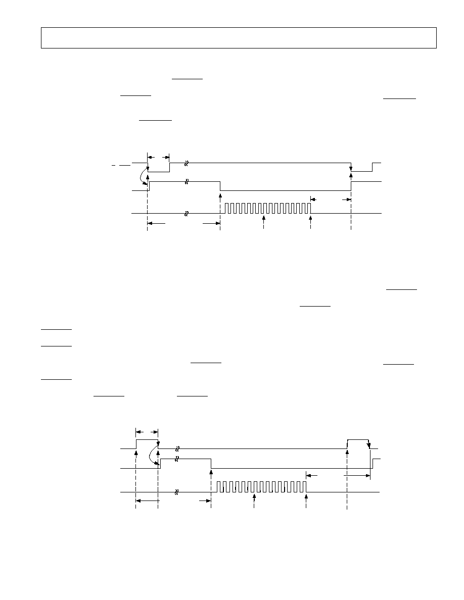
Conversion is initiated on the AD7896 by pulsing the CONVST
input. On the falling edge of CONVST, the on-chip track/hold
goes from track to hold mode and the conversion sequence is
started. The conversion clock for the part is generated inter-
nally using a laser-trimmed clock oscillator circuit. Conversion
time for the AD7896 is 8
µ
s in the high sampling mode (14
µ
s
for the auto sleep mode), and the track/hold acquisition time is
1.5
µ
s. To obtain optimum performance from the part, the read
operation should not occur during the conversion or during
400 ns prior to the next conversion. This allows the part to op-
erate at throughput rates up to 100 kHz and achieve data sheet
specifications (see Timing and Control Section).
CIRCUIT DESCRIPTION
Analog Input Section
The analog input range for the AD7896 is 0 V to V
DD.
The V
IN
pin drives the input to the track/hold amplifier directly. This al-
lows for a maximum output impedance of the circuit driving the
analog input of 1 k
. This ensures that the part will be settled
to 12-bit accuracy in the 1.5
µ
s acquisition time. This input is
benign with dynamic charging currents. The designed code
transitions occur on successive integer LSB values (i.e., 1 LSB,
2 LSB, 3 LSB . . . FS1 LSB). Output coding is straight (natu-
ral) binary with 1 LSB = FS/4096 = 3.3 V/4096 = 0.81 mV.
The ideal input/output transfer function is shown in Table I.
Table I. Ideal Input/Output Code Table for the AD7896
Analog Input
1
Code Transition
+FSR 1 LSB
2
(3.299194)
111 . . . 110 to 111 . . . 111
+FSR 2 LSB (3.298389)
111 . . . 101 to 111 . . . 110
+FSR/2 3 LSB (3.297583)
111 . . . 100 to 111 . . . 101
AGND + 3 LSB (0.002417)
000 . . . 010 to 000 . . . 011
AGND + 2 LSB (0.001611)
000 . . . 001 to 000 . . . 010
AGND + 1 LSB (0.000806)
000 . . . 000 to 000 . . . 001
NOTES
1
FSR is full-scale range and is 3.3 V with V
DD
= +3.3 V.
2
1 LSB = FSR/4096 = 0.81 mV with V
DD
= +3.3 V.
Track/Hold Section
The track/hold amplifier on the analog input of the AD7896 al-
lows the ADC to accurately convert an input sine wave of full-
scale amplitude to 12-bit accuracy. The input bandwidth of the
track/hold is greater than the Nyquist rate of the ADC even
when the ADC is operated at its maximum throughput rate of
100 kHz (i.e., the track/hold can handle input frequencies in
excess of 50 kHz).
The track/hold amplifier acquires an input signal to 12-bit accu-
racy in less than 1.5
µ
s. The operation of the track/hold is essen-
tially transparent to the user. With the high sampling operating
mode the track/hold amplifier goes from its tracking mode to its
hold mode at the start of conversion (i.e., the rising edge of
CONVST
). The aperture time for the track/hold (i.e., the delay
time between the external CONVST signal and the track/hold
actually going into hold) is typically 15 ns. At the end of conver-
sion (on the falling edge of BUSY) the part returns to its
tracking mode. The acquisition time of the track/hold amplifier
begins at this point. For the auto shutdown mode, the rising
edge of CONVST wakes up the part and the track and hold
amplifier goes from its tracking mode to its hold mode 6
µ
s after
the rising edge of CONVST ( provided that the CONVST high
time is less then 6
µ
s). Once again the part returns to its tracking
mode at the end of conversion when the BUSY signal goes low.
Timing and Control Section
Figure 2 shows the timing and control sequence required to ob-
tain optimum performance from the AD7896. In the sequence
shown, conversion is initiated on the falling edge of CONVST
and new data from this conversion is available in the output reg-
ister of the AD7896 8
µ
s later. Once the read operation has
taken place, a further 400 ns should be allowed before the next
falling edge of CONVST to optimize the settling of the track/
hold amplifier before the next conversion is initiated. With the
serial clock frequency at its maximum of 10 MHz (5 V opera-
tion), the achievable throughput rate for the part is 8
µ
s (conver-
sion time) plus 1.6
µ
s (read time) plus 0.4
µ
s (acquisition time).
This results in a minimum throughput time of 10
µ
s (equivalent
to a throughput rate of 100 kHz). A serial clock of less than 10
MHz can be used but this will in turn mean that the throughput
time will increase.
The read operation consists of sixteen serial clock pulses to the
output shift register of the AD7896. After sixteen serial clock
pulses the shift register is reset and the SDATA line is three-
stated. If there are more serial clock pulses after the sixteenth
clock, the shift register will be moved on past its reset state.
However, the shift register will be reset again on the falling edge
of the CONVST signal to ensure that the part returns to a
known state every conversion cycle. As a result, a read opera-
tion from the output register should not straddle across the fall-
ing edge of CONVST as the output shift register will be reset in
the middle of the read operation and the data read back into the
microprocessor will appear invalid.
The throughput rate of the part can be increased by reading
data during conversion. If the data is read during conversion, a
throughput time of 8
µ
s (conversion time) plus 1.5
µ
s (acquisi-
tion time) is achieved when a 10 MHz (5 V operation) serial
clock is being used. This minimum throughput time of 9.5
µ
s is
achieved with a slight reduction in performance from the
AD7896. The advantage of this arrangement is that when the
serial clock is significantly lower than 10 MHz the throughput
time for this arrangement will be significantly less than the
throughput time where the data is read after conversion. The
Signal to (Noise + Distortion) number is likely to degrade by
less than 1 dB while the code flicker from the part will also in-
crease (see AD7896 PERFORMANCE section).
AD7896
REV. B
7
OPERATING MODES
Mode 1 Operation (High Sampling Performance)
The timing diagram in Figure 2 is for optimum performance in
Operating Mode 1 where the falling edge of CONVST starts
conversion and puts the Track/Hold amplifier into its hold
mode. This falling edge of CONVST also causes the BUSY sig-
nal to go high to indicate that a conversion is taking place. The
BUSY signal goes low when the conversion is complete which is
8
µ
s max after the falling edge of CONVST, and new data from
this conversion is available in the output register of the AD7896.
A read operation accesses this data. This read operation consists
of 16 clock cycles, and the length of this read operation will de-
pend on the serial clock frequency. For the fastest throughput
rate (with a serial clock of 10 MHz 5 V operation) the read op-
eration will take 1.6
µ
s. The read operation must be complete at
least 400 ns before the falling edge of the next CONVST, and
this gives a total time of 10
µ
s for the full throughput time
(equivalent to 100 kHz). This mode of operation should be used
for high sampling applications.
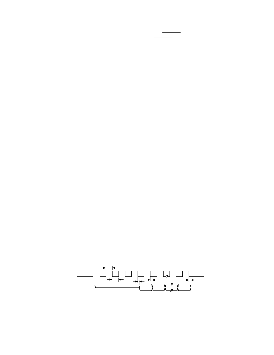
14
µ
s shown in diagram from the rising edge of CONVST. This
is because the Track/Hold amplifier goes into its hold mode on
the falling edge of CONVST and then the conversion will not be
complete for a further 8
µ
s. In this case the BUSY will be the
best indicator for when the conversion is complete. Even though
the part is in sleep mode, data can still be read from the part.
The read operation consists of 16 clock cycles as in Mode 1 op-
eration. For the fastest serial clock of 10 MHz 5 V operation the
read operation will take 1.6
µ
s, and this must be complete at
least 400 ns before the falling edge of the next CONVST to al-
low the Track/Hold amplifier to have enough time to settle.
This mode is very useful when the part is converting at a slow
rate as the power consumption will be significantly reduced
from that of Mode 1 operation.
Mode 2 Operation (Auto Sleep After Conversion)
The timing diagram in Figure 3 is for optimum performance in
Operating Mode 2 where the part automatically goes into sleep
mode once BUSY goes low after conversion and "wakes up" be-
fore the next conversion takes place. This is achieved by keeping
CONVST
low at the end of conversion whereas it was high at
the end of conversion for Mode 1 operation. The rising edge of
CONVST
"wakes up" the part. This wake-up time is 6
µ
s at
which point the Track/Hold amplifier goes into its hold mode.
The conversion takes 8
µ
s after this, provided the CONVST
has gone low, giving a total of 14
µ
s from the rising edge of
CONVST
to the conversion being complete which is indicated
by the BUSY going low. Note that since the wake-up time from
the rising edge of CONVST is 6
µ
s, when the CONVST pulse
width is greater than 6
µ
s the conversion will take more than the
t
CONVERT
= 8µs
CONVST
BUSY
SCLK
SERIAL READ
OPERATION
CONVERSION ENDS
8µs LATER
OUTPUT
SERIAL
SHIFT
REGISTER
IS RESET
CONVERSION IS
INITIATED AND
TRACK/HOLD GOES INTO
HOLD
t
1
= 40ns MIN
400ns MIN
t
1
t
CONVERT
= 8µs
READ OPERATION
SHOULD END 400ns
PRIOR TO NEXT
FALLING EDGE OF
CONVST
Figure 2. Mode 1 Timing Operation Diagram for High Sampling Performance
CONVST
BUSY
SCLK
SERIAL READ
OPERATION
CONVERSION
ENDS
14µs LATER
READ OPERATION
SHOULD END 400ns
PRIOR TO NEXT
FALLING EDGE OF
CONVST
OUTPUT
SERIAL
SHIFT
REGISTER
IS RESET
PART
WAKES
UP
CONVERSION
IS INITIATED
TRACK/HOLD
GOES INTO
HOLD
t
1
= 6µs
WAKE-UP
TIME
t
1
t
CONVERT
= 14µs
400ns MIN
Figure 3. Mode 2 Timing Diagram Where Automatic Sleep Function Is Initiated
REV. B
8
AD7896
Serial Interface
The serial interface to the AD7896 consists of just three wires, a
serial clock input (SCLK) and the serial data output (SDATA)
and a conversion status output (BUSY). This allows for an
easy-to-use interface to most microcontrollers, DSP processors
and shift registers.
Figure 4 shows the timing diagram for the read operation to the
AD7896. The serial clock input (SCLK) provides the clock
source for the serial interface. Serial data is clocked out from
the SDATA line on the falling edge of this clock and is valid on
both the rising and falling edges of SCLK. The advantage of
having the data valid on both the rising and falling edges of the
SCLK is so that it gives the user greater flexibility in interfacing
to the part and also so that a wider range of microprocessor and
microcontroller interfaces can be accommodated. This also ex-
plains the two timing figures t
4
and t
5
that are quoted on the dia-
gram. The time t
4
specifies how long after the falling edge of the
SCLK that the next data bit becomes valid whereas the time t
5
specifies how long after the falling edge of the SCLK that the
current data bit is valid for. The first leading zero is clocked out
on the first rising edge of SCLK, and note that the first zero
may be valid on the first falling edge of SCLK even though the
data access time is specified at 60 ns (5 V, A, B, J Versions only)
for the other bits ( and the SCLK high time will be 50 ns with a
10 MHz SCLK ). The reason that the first bit will be clocked
out faster than the other bits is due to the internal architecture
of the part. Sixteen clock pulses must be provided to the part to
access to full conversion result. The AD7896 provides four lead-
ing zeros followed by the 12-bit conversion result starting with
the MSB (DB11). The last data bit to be clocked out on the
penultimate falling clock edge is the LSB (DB0). On the six-
teenth falling edge of SCLK the LSB (DB0) will be valid for a
specified time to allow the bit to be read on the falling edge of
the SCLK, and then the SDATA line is disabled (three-stated).
After this last bit has been clocked out, the SCLK input should
remain low until the next serial data read operation. If there are
extra clock pulses after the sixteenth clock, the AD7896 will
start over again with outputting data from its output register,
and the data bus will no longer be three-stated even when the
clock stops. Provided the serial clock has stopped before the
next falling edge of CONVST, the AD7896 will continue to op-
erate correctly with the output shift register being reset on the
falling edge of CONVST. However, the SCLK line must be
low when CONVST goes low in order to reset the output shift
register correctly.
The serial clock input does not need to be continuous during
the serial read operation. The sixteen bits of data (four leading
zeros and 12-bit conversion result) can be read from the
AD7896 in a number of bytes. However, the SCLK input must
remain low between the two bytes.
The maximum SCLK frequency will be 10 MHz for 5 V opera-
tion (giving a throughput of 100 kHz) and at 2.7 V the maxi-
mum SCLK frequency will be less than 10 MHz to allow for the
longer data access time, t
4
(60 ns @ 5 V, 100 ns @ 2.7 V (A, B,
J Versions) 70 ns @ 5 V, (110 ns @ 2.7 V (S Version)). Note
that at 3.0 V operation (A, B, J Versions) an SCLK of 10 MHz
(throughput rate of 100 kHz) may be acceptable if the required
processor setup time is 0 ns (this may be possible with an ASIC
or FPGA). The data must be read in the next 10 ns which is
specified as the data hold time, t
5
, after the SCLK edge.
The AD7896 counts the serial clock edges to know which bit
from the output register should be placed on the SDATA out-
put. To ensure that the part does not lose synchronization, the
serial clock counter is reset on the falling edge of the CONVST
input provided the SCLK line is low. The user should ensure
that a falling edge on the CONVST input does not occur while
a serial data read operation is in progress.
MICROPROCESSOR/MICROCONTROLLER INTERFACE
The AD7896 provides a three-wire serial interface that can be
used for connection to the serial ports of DSP processors and
microcontrollers. Figures 5 through 8 show the AD7896 inter-
faced to a number of different microcontrollers and DSP pro-
cessors. The AD7896 accepts an external serial clock and as a
result, in all interfaces shown here, the processor/controller is
configured as the master, providing the serial clock, with the
AD7896 configured as the slave in the system.
AD78968051 Interface
Figure 5 shows an interface between the AD7896 and the 8X51/
L51 microcontroller. The 8X51/L51 is configured for its Mode
0 serial interface mode. The diagram shows the simplest form
of the interface where the AD7896 is the only part connected to
the serial port of the 8X51/L51 and, therefore, no decoding of
the serial read operations is required.
t
2
4 LEADING ZEROS
DOUT (O/P)
SCLK (I/P)
t
6
1
2
3
4
5
6
15
16
DB0
DB10
DB11
3-STATE
t
5
t
3
t
4
3-STATE
t
2
=
t
3
= 40ns MIN,
t
4
= 60ns MAX,
t
5
= 10ns MIN,
t
6
= 50ns MAX @ 5v, A, B, VERSIONS
Figure 4. Data Read Operation
AD7896
REV. B
9
The BUSY line can be connected to the IRQ line of the
68HC11/L11 if an interrupt driven system is preferred. These
two options are shown in the diagram.
The serial clock rate from the 68HC11/L11 is limited to signifi-
cantly less than the allowable input serial clock frequency with
which the AD7896 can operate. As a result, the time to read
data from the part will actually be longer than the conversion
time of the part. This means that the AD7896 cannot run at its
maximum throughput rate when used with the 68HC11/L11.
AD7896
SDATA
SCLK
BUSY
SCK
MISO
68HC11/L11
PC2 OR
IRQ
Figure 6. AD7896 to 68HC11/L11 Interface
AD7896ADSP-2103/ADSP-2105 Interface
An interface circuit between the AD7896 and the ADSP-2103/
ADSP-2105 DSP processor is shown in Figure 7. In the inter-
face shown, the RFS1 output from the ADSP-2103/ADSP-
2105s SPORT1 serial port is used to gate the serial clock
(SCLK1) of the ADSP-2103/ADSP-2105 before it is applied to
the SCLK input of the AD7896. The RFS1 output is config-
ured for active high operation. The BUSY line from the
AD7896 is connected to the IRQ2 line of the ADSP-2103/
ADSP-2105 so that at the end of conversion an interrupt is gen-
erated telling the ADSP-2103/ADSP-2105 to initiate a read op-
eration. The interface ensures a noncontinuous clock for the
AD7896's serial clock input, with only sixteen serial clock pulses
provided and the serial clock line of the AD7896 remaining low
between data transfers. The SDATA line from the AD7896 is
connected to the DR1 line of the ADSP-2103/ADSP-2105's
serial port.
The timing relationship between the SCLK1 and RFS1 outputs
of the ADSP-2103/ADSP-2105 are such that the delay between
the rising edge of the SCLK1 and the rising edge of an active
high RFS1 is up to 30 ns. There is also a requirement that data
must be set up 10 ns prior to the falling edge of the SCLK1 to
be read correctly by the ADSP-2103/ADSP-2105. The data ac-
cess time for the AD7896 is 60 ns (5 V (A, B versions)) from
the rising edge of its SCLK input. Assuming a 10 ns propaga-
tion delay through the external AND gate, the high time of the
SCLK1 output of the ADSP-2105 must be
(30 + 60 +10
+10) ns, i.e.,
110 ns. This means that the serial clock fre-
quency with which the interface of Figure 7 can work is limited
to 4.5 MHz. However, there is an alternative method which al-
lows for the ADSP-2105 SCLK1 to run at 5 MHz (which is the
max serial clock frequency of the SCLK1 output). The arrange-
ment is where the first leading zero of the data stream from the
AD7896 cannot be guaranteed to be clocked into the ADSP-
2105 due to the combined delay of the RFS signal and the data
access time of the AD7896. In most cases this is acceptable as
there will still be three leading zeros followed by the 12 data
bits. For the ADSP-2103 the SCLK1 frequency will need to be
limited to < 4 MHz to account for the 100 ns data access time
of the AD7896 at 3 V.
To chip select the AD7896 in systems where more than one de-
vice is connected to the 8X51/L51's serial port, a port bit, con-
figured as an output, from one of the 8X51/L51's parallel ports
can be used to gate on or off the serial clock to the AD7896. A
simple AND function on this port bit and the serial clock from
the 8X51/L51 will provide this function. The port bit should be
high to select the AD7896 and low when it is not selected.
The end of conversion is monitored by using the BUSY signal
which is shown in the interface diagram of Figure 5. With the
BUSY line from the AD7896 connected to the Port P1.2 of the
8X51/L51 so the BUSY line can be polled by the 8X51/L51.
The BUSY line can be connected to the INT1 line of the 8X51/
L51 if an interrupt driven system is preferred. These two op-
tions are shown on the diagram.
Note also that the AD7896 outputs the MSB first during a read
operation while the 8X51/L51 expects the LSB first. Therefore,
the data which is read into the serial buffer needs to be rear-
ranged before the correct data format from the AD7896 appears
in the accumulator.
The serial clock rate from the 8X51/L51 is limited to signifi-
cantly less than the allowable input serial clock frequency with
which the AD7896 can operate. As a result, the time to read
data from the part will actually be longer than the conversion
time of the part. This means that the AD7896 cannot run at its
maximum throughput rate when used with the 8X51/L51.
AD7896
SDATA
SCLK
BUSY
P3.0
P3.1
8X51/L51
P1.2
OR
INT1
Figure 5. AD7896 to 8X51/L51 Interface
AD789668HC11/L11 Interface
An interface circuit between the AD7896 and the 68HC11/L11
microcontroller is shown in Figure 6. For the interface shown,
the 68HC11/L11 SPI port is used and the 68HC11/L11 is con-
figured in its single-chip mode. The 68HC11/L11 is configured
in the master mode with its CPOL bit set to a logic zero and its
CPHA bit set to a logic one. As with the previous interface, the
diagram shows the simplest form of the interface where the
AD7896 is the only part connected to the serial port of the
68HC11/L11 and, therefore, no decoding of the serial read
operations is required.
Once again, to chip select the AD7896 in systems where more
than one device is connected to the 68HC11/L11's serial port, a
port bit, configured as an output, from one of the 68HC11/
L11's parallel ports can be used to gate on or off the serial clock
to the AD7896. A simple AND function on this port bit and
the serial clock from the 68HC11/L11 will provide this function.
The port bit should be high to select the AD7896 and low when
it is not selected.
The end of conversion is monitored by using the BUSY signal
which is shown in the interface diagram of Figure 6. With the
BUSY line from the AD7896 connected to the Port PC0 of the
68HC11/L11 the BUSY line can be polled by the 68HC11/L11.
REV. B
10
AD7896
Figure 9 shows a histogram plot for 8192 conversions of a dc in-
put using the AD7896 with 3.3 V supply. The analog input was
set at the center of a code transition. It can be seen that almost
all the codes appear in the one output bin indicating very good
noise performance from the ADC. The rms noise performance
for the AD7896 for the plot below was 111
µ
V.
9000
0
2000
1000
3000
4000
5000
6000
7000
8000
1005
1006
CODE
F
SAMPLE
= 95kHz,
F
SCLK
= 8.33 MHz,
AIN CENTERED ON CODE 1005,
rms NOISE = 0.138LSBS
OCCURRENCE
Figure 9. Histogram of 8192 Conversions of a DC Input
The same data is presented in Figure 10 as in Figure 9 except
that in this case the output data read for the device occurs dur-
ing conversion. This has the effect of injecting noise onto the
die while bit decisions are being made and this increases the
noise generated by the AD7896. The histogram plot for 8192
conversions of the same dc input now shows a larger spread of
codes with the rms noise for the AD7896 increasing to 279
µ
V .
This effect will vary depending on where the serial clock edges
appear with respect to the bit trials of the conversion process. It
is possible to achieve the same level of performance when read-
ing during conversion as when reading after conversion depend-
ing on the relationship of the serial clock edges to the bit trial
points.
8000
0
2000
1000
1004
4000
3000
5000
6000
7000
1005
1006
CODE
OCCURRENCE
F
SAMPLE
= 95 kHz,
F
SCLK
= 8.33MHz,
AIN CENTERED ON
CODE 1005, rms
NOISE = 0.346 LSBS
Figure 10. Histogram of 8192 Conversions with Read
During Conversion
Another alternative scheme is to configure the ADSP-2103/
ADSP-2105 such that it accepts an external noncontinuous se-
rial clock. In this case, an external noncontinuous serial clock is
provided which drives the serial clock inputs of both the ADSP-
2103/ADSP-2105 and the AD7896. In this scheme, the serial
clock frequency is limited to 10 MHz by the AD7896.
AD7896
SDATA
SCLK
BUSY
SCLK1
DR1
ADSP-2103/5
IRQ2
RFS1
Figure 7. AD7896 to ADSP-2103 /5 Interface
AD7896DSP56002/L002 Interface
Figure 8 shows an interface circuit between the AD7896 and the
DSP56002/L002 DSP processor. The DSP56002/L002 is con-
figured for normal mode asynchronous operation with gated
clock. It is also set up for a 16-bit word with SCK as gated
clock output. In this mode, the DSP56002/L002 provides six-
teen serial clock pulses to the AD7896 in a serial read operation.
The DSP56002/L002 assumes valid data on the first falling edge
of SCK so the interface is simply two-wire as shown in Figure 8.
The BUSY line from the AD7896 is connected to the MODA/
IRQA
input of the DSP56002/L002 so that an interrupt will be
generated at the end of conversion. This ensures that the read
operation will take place after conversion is finished.
AD7896
SDATA
SCLK
BUSY
SCK
SDR
DSP56002/L002
MODA /
IRQA
Figure 8. AD7896 to DSP56002/L002 Interface
AD7896 PERFORMANCE
Linearity
The linearity of the AD7896 is determined by the on-chip 12-
bit D/A converter. This is a segmented DAC which is laser
trimmed for 12-bit integral linearity and differential linearity.
Typical relative accuracy numbers for the part are
±
1/4 LSB
while the typical DNL errors are
±
1/2 LSB.
Noise
In an A/D converter, noise exhibits itself as code uncertainty in
dc applications and as the noise floor (in an FFT, for example)
in ac applications. In a sampling A/D converter like the
AD7896, all information about the analog input appears in the
baseband from dc to 1/2 the sampling frequency. The input
bandwidth of the track/hold exceeds the Nyquist bandwidth
and, therefore, an antialiasing filter should be used to remove
unwanted signals above f
S
/2 in the input signal in applications
where such signals exist.
AD7896
REV. B
11
Dynamic Performance (Mode 1 Only)
With a combined conversion and acquisition time of 9.5
µ
s, the
AD7896 is ideal for wide bandwidth signal processing applica-
tions. These applications require information on the ADC's ef-
fect on the spectral content of the input signal. Signal to (Noise
+ Distortion), Total Harmonic Distortion, Peak Harmonic or
Spurious Noise and Intermodulation Distortion are all specified.
Figure 11 shows a typical FFT plot of a 10 kHz, 0 V to +3.3 V
input after being digitized by the AD7896 operating at a
102.4 kHz sampling rate. The Signal to (Noise + Distortion)
Ratio is 71.5 dB and the Total Harmonic Distortion is 83 dB.
0
120
51200
60
100
10240
80
0
20
40
40960
30720
20480
F
SAMPLE
= 102.4 kHz
F
IN
= 10kHz
SNR = 71.54dB
THD = 82.43dB
FREQUENCY Hz
dB
Figure 11. AD7896 FFT Plot
Effective Number of Bits
The formula for Signal to (Noise + Distortion) Ratio (See Ter-
minology section) is related to the resolution or number of bits
in the converter. Rewriting the formula, below, gives a measure
of performance expressed in effective number of bits (N):
N = (SNR 1.76)/6.02
where SNR is Signal to (Noise + Distortion) Ratio.
The effective number of bits for a device can be calculated from
its measured Signal to (Noise + Distortion) Ratio. Figure 12
shows a typical plot of effective number of bits versus frequency
for the AD7896 from dc to f
SAMPLING
/2. The sampling fre-
quency is 102.4 kHz. The plot shows that the AD7896 converts
an input sine wave of 51.2 kHz to an effective numbers of bits of
11.25 which equates to a Signal to (Noise + Distortion) level
of 69 dB.
12.00
0
51.2
25.6
11.75
11.50
11.25
11.00
INPUT FREQUENCY kHz
EFFECTIVE NUMBER OF BITS
Figure 12. Effective Number of Bits vs. Frequency
Power Considerations
In the automatic power-down mode then the part may be oper-
ated at a sample rate which is considerably less than 100 kHz. In
this case the power consumption will be reduced and will de-
pend on the sample rate. Figure 13 shows a graph of the power
consumption versus sampling rates from 10 Hz to 1 kHz in the
automatic power-down mode. The conditions are 2.7 V supply
25
°
C, serial clock frequency of 8.33 MHz and the data was read
after conversion.
200
0
1000
120
40
100
80
10
160
SAMPLING RATE IN Hz
POWER
µ
W
F
SCLK
= 8.33 MHz
Figure 13. Power vs. Sample Rate in Auto Power-Down
Mode
REV. B
12
AD7896
OUTLINE DIMENSIONS
Dimensions shown in inches and (mm).
8-Lead Plastic DIP
(N-8)
PIN 1
0.280 (7.11)
0.240 (6.10)
4
5
8
1
SEATING
PLANE
0.060 (1.52)
0.015 (0.38)
0.130
(3.30)
MIN
0.210
(5.33)
MAX
0.160 (4.06)
0.115 (2.93)
0.430 (10.92)
0.348 (8.84)
0.022 (0.558)
0.014 (0.356)
0.070 (1.77)
0.045 (1.15)
0.100
(2.54)
BSC
0.325 (8.25)
0.300 (7.62)
0.015 (0.381)
0.008 (0.204)
0.195 (4.95)
0.115 (2.93)
8-Lead Cerdip
(Q-8)
0.320 (8.13)
0.290 (7.37)
0.015 (0.38)
0.008 (0.20)
15
°
0
°
0.005 (0.13) MIN
0.055 (1.4) MAX
1
PIN 1
4
5
8
0.310 (7.87)
0.220 (5.59)
0.405 (10.29) MAX
0.200
(5.08)
MAX
SEATING
PLANE
0.023 (0.58)
0.014 (0.36)
0.070 (1.78)
0.030 (0.76)
0.060 (1.52)
0.015 (0.38)
0.150
(3.81)
MIN
0.200 (5.08)
0.125 (3.18)
0.100
(2.54)
BSC
8-Lead Small Outline
(SO-8)
0.0098 (0.25)
0.0075 (0.19)
0.0500 (1.27)
0.0160 (0.41)
8
°
0
°
0.0196 (0.50)
0.0099 (0.25)
x 45
°
PIN 1
0.1574 (4.00)
0.1497 (3.80)
0.2440 (6.20)
0.2284 (5.80)
4
5
1
8
0.0192 (0.49)
0.0138 (0.35)
0.0500
(1.27)
BSC
0.0688 (1.75)
0.0532 (1.35)
0.0098 (0.25)
0.0040 (0.10)
0.1968 (5.00)
0.1890 (4.80)
PRINTED IN U.S.A.
C1962a129/96