 | ÐлекÑÑоннÑй компоненÑ: AD795 | СкаÑаÑÑ:  PDF PDF  ZIP ZIP |
Äîêóìåíòàöèÿ è îïèñàíèÿ www.docs.chipfind.ru
CONNECTION DIAGRAMS
8-Pin Plastic Mini-DIP (N) Package
OUTPUT VOLTAGE SWING Volts p-p
LOAD RESISTANCE
30
0
10
10k
20
10
100
1k
Vs = ±15V
25
15
5
8-Pin SOIC (R) Package
1
2
3
4
8
7
6
5
AD795
NC
IN
+IN
V
S
NC
+V
S
OUTPUT
NC
NC = NO CONNECT
REV. A
Information furnished by Analog Devices is believed to be accurate and
reliable. However, no responsibility is assumed by Analog Devices for its
use, nor for any infringements of patents or other rights of third parties
which may result from its use. No license is granted by implication or
otherwise under any patent or patent rights of Analog Devices.
a
Low Power, Low Noise
Precision FET Op Amp
AD795
One Technology Way, P.O. Box 9106, Norwood, MA 02062-9106, U.S.A.
Tel: 617/329-4700
Fax: 617/326-8703
FEATURES
Low Power Replacement for Burr-Brown
OPA-111, OPA-121 Op Amps
Low Noise
2.5 V p-p max, 0.1 Hz to 10 Hz
11 nV/
Hz max at 10 kHz
0.6 fA/
Hz at 1 kHz
High DC Accuracy
250 V max Offset Voltage
3 V/ C max Drift
1 pA max Input Bias Current
Low Power: 1.5 mA max Supply Current
Available in Low Cost Plastic Mini-DIP and Surface
Mount (SOIC) Packages
APPLICATIONS
Low Noise Photodiode Preamps
CT Scanners
Precision l-to-V Converters
PRODUCT DESCRIPTION
The AD795 is a low noise, precision, FET input operational
amplifier. It offers both the low voltage noise and low offset drift
of a bipolar input op amp and the very low bias current of a
FET-input device. The 10
14
common-mode impedance
insures that input bias current is essentially independent of
common-mode voltage and supply voltage variations.
The AD795 has both excellent dc performance and a guaran-
teed and tested maximum input voltage noise. It features 1 pA
maximum input bias current and 250
µ
V maximum offset volt-
age, along with low supply current of 1.5 mA max.
1k
10
1
10
100
10k
1k
100
FREQUENCY Hz
VOLTAGE NOISE SPECTRAL DENSITY nV/
Hz
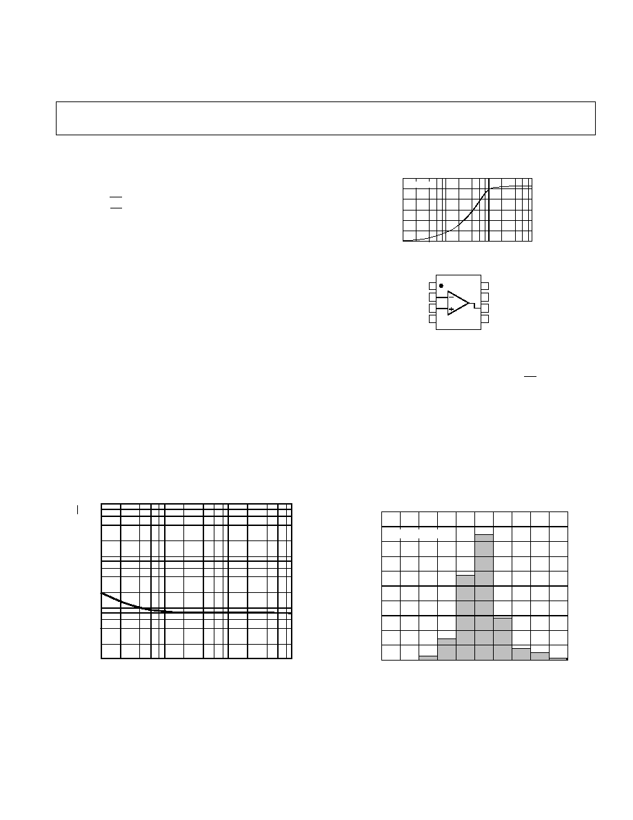
AD795 Voltage Noise Spectral Density
Furthermore, the AD795 features a guaranteed low input noise
of 2.5
µ
V p-p (0.1 Hz to 10 Hz) and a 11 nV/
Hz
max noise
level at 10 kHz. The AD795 has a fully specified and tested
input offset voltage drift of only 3
µ
V/
°
C max.
The AD795 is useful for many high input impedance, low noise
applications. The AD795J and AD795K are rated over the
commercial temperature range of 0
°
C to +70
°
C.
The AD795 is available in 8-pin plastic mini-DIP and 8-pin
surface mount (SOIC) packages.
50
0
5
4
10
5
30
20
40
4
3
2
1
0
1
2
3
INPUT OFFSET VOLTAGE DRIFT
µ
V/
°
C
PERCENTAGE OF UNITS
SAMPLE SIZE = 570
Typical Distribution of Average Input Offset Voltage Drift

REV. A
2
AD795SPECIFICATIONS
AD795JN/JR
AD795K
Parameter
Conditions
Min
Typ
Max
Min
Typ
Max
Units
INPUT OFFSET VOLTAGE
1
Initial Offset
100
500
50
250
µ
V
Offset
T
MIN
T
MAX
300
1000
100
400
µ
V
vs. Temperature
3
10
1
3
µ
V/
°
C
vs. Supply (PSRR)
86
110
90
110
dB
vs. Supply (PSRR)
T
MIN
T
MAX
84
100
87
100
dB
INPUT BIAS CURRENT
2
Either Input
V
CM
= 0 V
1
2/3
1
1
pA
Either Input @ T
MAX
=
V
CM
= 0 V
23
23
pA
Either Input
V
CM
= +10 V
1
1
pA
Offset Current
V
CM
= 0 V
0.1
1.0
0.1
0.6
pA
Offset Current @ T
MAX
=
V
CM
= 0 V
2
2
pA
OPEN-LOOP GAIN
V
O
=
±
10 V
R
LOAD
10 k
110
120
110
120
dB
R
LOAD
10 k
100
108
100
108
dB
INPUT VOLTAGE NOISE
0.1 Hz to 10 Hz
1.0
3.3
1.0
2.5
µ
V p-p
f = 10 Hz
20
50
20
40
nV/
Hz
f = 100 Hz
12
40
12
30
nV/
Hz
f = 1 kHz
11
17
11
15
nV/
Hz
f = 10 kHz
9
11
9
11
nV/
Hz
INPUT CURRENT NOISE
f = 0.1 Hz to 10 Hz
13
13
fA p-p
f = 1 kHz
0.6
0.6
fA/
Hz
FREQUENCY RESPONSE
Unity Gain, Small Signal
G = 1
1.6
1.6
MHz
Full Power Response
V
O
= 20 V p-p
R
LOAD
= 2 k
16
16
kHz
Slow Rate, Unity Gain
V
OUT
= 20 V p-p
R
LOAD
= 2 k
1
1
V/
µ
s
SETTLING TIME
3
To 0.1%
10 V Step
10
10
µ
s
To 0.01%
10 V Step
11
11
µ
s
Overload Recovery
4
50% Overdrive
2
2
µ
s
Total Harmonic
f = 1 kHz
Distortion
R1
10 k
V
O
= 3 V rms
108
108
dB
INPUT IMPEDANCE
Differential
V
DIFF
=
±
1 V
10
12
2
10
12
2
pF
Common Mode
10
14
2.2
10
14
2.2
pF
INPUT VOLTAGE RANGE
Differential
5
±
20
±
20
V
Common-Mode Voltage
±
10
±
11
±
10
±
11
V
Over Max Operating Temperature
±
10
±
10
V
Common-Mode Rejection Ratio
V
CM
=
±
10 V
90
110
94
110
dB
T
MIN
T
MAX
86
100
90
100
dB
OUTPUT CHARACTERISTICS
Voltage
R
LOAD
2 k
V
S
4
V
S
2.5
V
S
4
V
S
2.5
V
T
MIN
T
MAX
V
S
4
V
S
4
V
Current
V
OUT
=
±
10 V
±
5
±
10
±
5
±
10
mA
Short Circuit
±
15
±
15
mA
POWER SUPPLY
Rated Performance
±
15
±
15
V
Operating Range
±
4
±
18
±
4
±
18
V
Quiescent Current
1.3
1.5
1.3
1.5
mA
(@ +25 C and 15 V dc unless otherwise noted)

NOTES
1
Input offset voltage specifications are guaranteed after 5 minutes of operation at T
A
= +25
°
C.
2
Bias current specifications are guaranteed maximum at either input after 5 minutes of operation at T
A
= +25
°
C. For higher temperature, the current doubles every 10
°
C.
3
Gain = 1, R1 = 10 k
.
4
Defined as the time required for the amplifier's output to return to normal operation after removal of a 50% overload from the amplifier input.
5
Defined as the maximum continuous voltage between the inputs such that neither input exceeds
±
10 V from ground.
All min and max specifications are guaranteed.
Specifications subject to change without notice.
AD795
REV. A
3
ABSOLUTE MAXIMUM RATINGS
1
Supply Voltage . . . . . . . . . . . . . . . . . . . . . . . . . . . . . . . .
±
18 V
Internal Power Dissipation
2
(@ T
A
= +25
°
C)
SOIC Package . . . . . . . . . . . . . . . . . . . . . . . . . . . . 500 mW
8-Pin Mini-DIP Package . . . . . . . . . . . . . . . . . . . . 750 mW
Input Voltage . . . . . . . . . . . . . . . . . . . . . . . . . . . . . . . . . . .
±
V
S
Output Short Circuit Duration . . . . . . . . . . . . . . . . Indefinite
Differential Input Voltage . . . . . . . . . . . . . . . . . . +V
S
and V
S
Storage Temperature Range (N, R) . . . . . . . 65
°
C to +125
°
C
Operating Temperature Range
AD795J/K . . . . . . . . . . . . . . . . . . . . . . . . . . . 0
°
C to +70
°
C
NOTES
1
Stresses above those listed under "Absolute Maximum Ratings" may cause
permanent damage to the device. This is a stress rating only and functional
operation of the device at these or any other conditions above those indicated in the
operational section of this specification is not implied. Exposure to absolute
maximum rating conditions for extended periods may affect device reliability.
2
8-Pin Plastic Mini-DIP Package:
JA
= 100
°
C/Watt
8-Pin Small Outline Package:
JA
= 155
°
C/Watt
ESD SUSCEPTIBILITY
ESD (electrostatic discharge) sensitive device. Electrostatic
charges as high as 4000 volts, which readily accumulate on the
human body and on test equipment, can discharge without
detection. Although the AD795 features proprietary ESD pro-
tection circuitry, permanent damage may still occur on these
devices if they are subjected to high energy electrostatic dis-
charges. Therefore, proper ESD precautions are recommended
to avoid any performance degradation or loss of functionality.
ORDERING GUIDE
Model
Temperature Range
Package Option*
AD795JN
0
°
C to +70
°
C
N-8
AD795KN
0
°
C to +70
°
C
N-8
AD795JR
0
°
C to +70
°
C
R-8
*N = Plastic mini-DIP; R = SOIC package.
AD795Typical Characteristics
REV. A
4
SUPPLY VOLTAGE ±Volts
INPUT COMMON MODE RANGE ±Volts
20
0
0
20
15
5
5
10
10
15
R
L
= 10k
+V
IN
V
IN
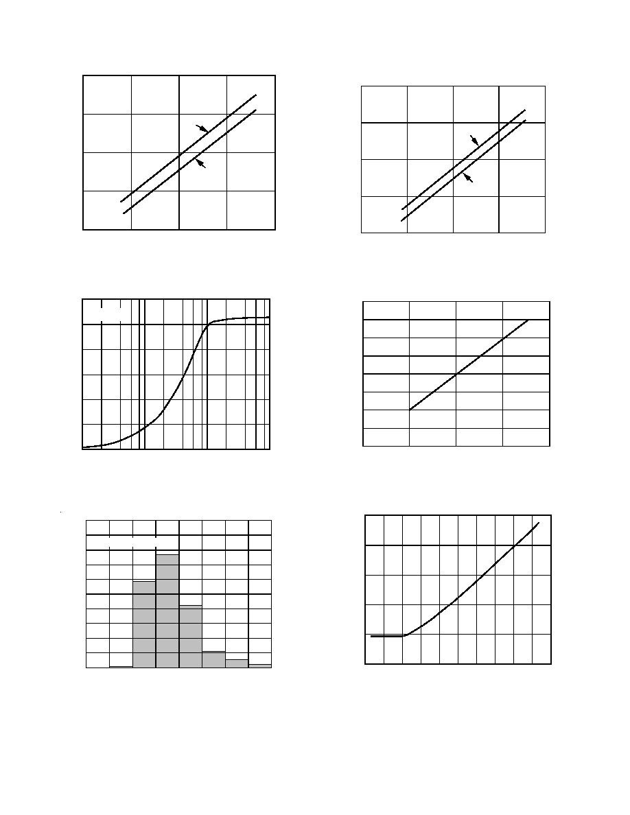
Figure 1. Common-Mode Voltage Range vs. Supply
OUTPUT VOLTAGE SWING Volts p-p
LOAD RESISTANCE
30
0
10
10k
20
10
100
1k
V
s
= ±15V
25
15
5
Figure 3. Output Voltage Swing vs. Load Resistance
INPUT BIAS CURRENT pA
PERCENTAGE OF UNITS
50
0
2
10
0
30
20
40
1.5
1
.5
SAMPLE SIZE = 1058
Figure 5. Typical Distribution of Input Bias Current
OUTPUT VOLTAGE RANGE ±Volts
SUPPLY VOLTAGE ±Volts
20
0
0
20
15
5
5
10
10
15
R
L
= 10k
+V
OUT
V
OUT
Figure 2. Output Voltage Range vs. Supply Voltage
0
20
5
15
10
SUPPLY VOLTAGE ±Volts
INPUT BIAS CURRENT pA
1.0
0.60
0.70
0.65
0.80
0.75
0.85
0.90
0.95
Figure 4. Input Bias Current vs. Supply
10
9
10
14
140
10
11
10
13
40
10
12
60
10
10
120
100
80
60
40
20
0
20
INPUT BIAS CURRENT Amps
TEMPERATURE
°
C
Figure 6. Input Bias Current vs. Temperature
AD795
REV. A
5
DIFFERENTIAL INPUT VOLTAGE ±Volts
INPUT BIAS CURRENT Amperes
6
5
4
3
2
1
0
1
2
4
I
IN
+I
IN
5
6
3
10
4
10
5
10
6
10
7
10
8
10
9
10
10
10
11
10
12
10
13
10
14
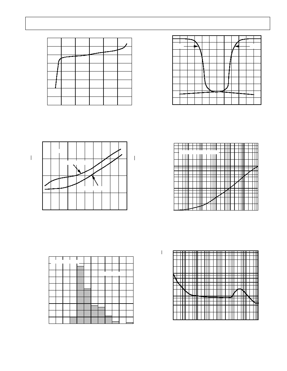
Figure 8. Input Bias Current vs. Differential Input Voltage
VOLTAGE NOISE
µ
V p-p
SOURCE RESISTANCE
1k
10
1.0
10
3
10
4
10
9
10
8
10
7
10
6
10
5
Noise Bandwidth: 0.1 to 10Hz
100
Figure 10. Input Voltage Noise vs. Source Resistance
FREQUENCY Hz
1k
10
1.0
100
1
10
10M
1M
100k
10k
1k
100
VOLTAGE NOISE (REFERRED TO INPUT) nV/
Hz
Figure 12. Input Voltage Noise Spectral Density
1.00
0.60
+15
0.70
0.65
10
15
0.80
0.75
0.85
0.90
0.95
+10
+5
0
5
INPUT BIAS CURRENT
pA
COMMON MODE VOLTAGE Volts
Figure 7. Input Bias Current vs. Common-Mode Voltage
60
140
40
100
120
80
60
40
20
0
20
TEMPERATURE
°
C
VOLTAGE NOISE nV/
Hz
15
12.5
10
7.5
5
100
10
1.0
0.1
0.01
CURRENT NOISE fA/
Hz
VOLTAGE NOISE
CURRENT NOISE
f = 1kHz
Figure 9. Voltage and Current Noise Spectral Density vs.
Temperature
0.1 TO 10Hz INPUT VOLTAGE NOISE p-p
µ
V
PERCENTAGE OF UNITS
50
0
3
10
0
30
20
40
2
1
SAMPLE SIZE = 344
f = 0.1 TO 10Hz
Figure 11. Typical Distribution of Input Voltage Noise