 | ÐлекÑÑоннÑй компоненÑ: AD8004AR | СкаÑаÑÑ:  PDF PDF  ZIP ZIP |
Ad8004 Data Sheet
REV. B
Information furnished by Analog Devices is believed to be accurate and
reliable. However, no responsibility is assumed by Analog Devices for its
use, nor for any infringements of patents or other rights of third parties
which may result from its use. No license is granted by implication or
otherwise under any patent or patent rights of Analog Devices.
a
AD8004
One Technology Way, P.O. Box 9106, Norwood, MA 02062-9106, U.S.A.
Tel: 781/329-4700
World Wide Web Site: http://www.analog.com
Fax: 781/326-8703
© Analog Devices, Inc., 1999
Quad 3000 V/ s, 35 mW
Current Feedback Amplifier
FEATURES
High Speed
250 MHz 3 dB Bandwidth (G = +1)
3000 V/ s Slew Rate
21 ns Settling Time to 0.1%
1.8 ns Rise Time for 2 V Step
Low Power
3.5 mA/Amp Power Supply Current (35 mW/Amp)
Single Supply Operation
Fully Specified for +5 V Supply
Good Video Specifications (R
L
= 150 , G = +2)
Gain Flatness 0.1 dB to 30 MHz
0.04% Differential Gain Error
0.10 Differential Phase Error
Low Distortion
78 dBc THD at 5 MHz
61 dBc THD at 20 MHz
High Output Current of 50 mA
Available in a 14-Lead Plastic DIP and SOIC
APPLICATIONS
Image Scanners
Active Filters
Video Switchers
Special Effects
PRODUCT DESCRIPTION
The AD8004 is a quad, low power, high speed amplifier designed
to operate on single or dual supplies. It utilizes a current feed-
back architecture and features high slew rate of 3000 V/
µ
s
making the AD8004 ideal for handling large amplitude pulses.
Additionally, the AD8004 provides gain flatness of 0.1 dB to
FREQUENCY MHz
+1
4
9
1
500
10
40
100
3
2
1
0
5
6
7
8
NORMALIZED FREQUENCY RESPONSE dB
NORMALIZED FLATNESS dB
+0.1
0
0.1
0.2
0.3
0.4
0.5
5V
S
+5V
S
+5V
S
5V
S
G = +2
V
IN
= 50mV rms
R
L
= 100
R
F
= 1.10k
R PACKAGE
Figure 1. Frequency Response and Flatness, G = +2
CONNECTION DIAGRAM
Plastic DIP (N) and
SOIC (R) Packages
14
13
12
11
10
9
8
1
2
3
4
7
6
5
1
2
3
4
AD8004
(TOP VIEW)
OUTPUT
IN
+IN
+V
S
+IN
IN
OUTPUT
V
S
+IN
IN
OUTPUT
OUTPUT
IN
+IN
30 MHz while offering differential gain and phase error of
0.04% and 0.10
°
. This makes the AD8004 suitable for video
electronics such as cameras and video switchers.
The AD8004 offers low power of 3.5 mA/amplifier and can run
on a single +4 V to +12 V power supply, while being capable of
delivering up to 50 mA of load current. All this is offered in a
small 14-lead plastic DIP or 14-lead SOIC package. These
features make this amplifier ideal for portable and battery pow-
ered applications where size and power are critical.
The outstanding bandwidth of 250 MHz along with 3000 V/
µ
s
of slew rate make the AD8004 useful in many general purpose,
high speed applications where dual power supplies of up to
±
6 V and single supplies from 4 V to 12 V are needed. The
AD8004 is available in the industrial temperature range of 40
°
C
to +85
°
C.
0.04
0.03
0.02
0.01
0.00
0.01
0.02
0.03
0.04
1
ST
DIFF GAIN %
0.12
0.10
0.08
0.06
0.04
0.02
0.00
0.02
0.04
DIFF PHASE Degrees
2
ND
3
RD
4
TH
5
TH
6
TH
7
TH
8
TH
9
TH
10
TH
11
TH
1
ST
2
ND
3
RD
4
TH
5
TH
6
TH
7
TH
8
TH
9
TH
10
TH
11
TH
80 IRE
R
L
= 150
V
S
= 5V
R
F
= 1.21k
80 IRE
R
L
= 150
V
S
= 5V
R
F
= 1.21k
Figure 2. Differential Gain/Differential Phase

REV. B
2
AD8004SPECIFICATIONS
AD8004A
Parameter
Conditions
Min
Typ
Max
Units
DYNAMIC PERFORMANCE
3 dB Bandwidth, N Package
G = +2, R
F
= 698
185
MHz
G = +1
, R
F
= 806
250
MHz
Bandwidth for 0.1 dB Flatness
G = +2
30
MHz
Slew Rate
G = +2, V
O
= 4 V Step
3000
V/
µ
s
G = 2, V
O
= 4 V Step
2000
V/
µ
s
Settling Time to 0.1%
G = +2, V
O
= 2 V Step
21
ns
Rise & Fall Time (10% to 90%)
G = +2, V
O
= 2 V Step
1.8
ns
NOISE/HARMONIC PERFORMANCE
Total Harmonic Distortion
f
C
= 5 MHz, V
O
= 2 V p-p, R
L
= 1 k
78
dBc
Crosstalk, R Package, Worst Case
f = 5 MHz, G = +2, R
L
= 1 k
69
dB
Crosstalk, N Package, Worst Case
f = 5 MHz, G = +2, R
L
= 1 k
64
dB
Input Voltage Noise
f = 10 kHz
1.5
nV/
Hz
Input Current Noise
f = 10 kHz, +In
38
pA/
Hz
In
38
pA/
Hz
Differential Gain Error
NTSC, G = +2, R
L
= 150
, R
F
= 1.21 k
0.04
%
Differential Phase Error
NTSC, G = +2, R
L
= 150
, R
F
= 1.21 k
0.10
Degree
Differential Gain Error
NTSC, G = +2, R
L
= 1 k
, R
F
= 1.21 k
0.01
%
Differential Phase Error
NTSC, G = +2, R
L
= 1 k
, R
F
= 1.21 k
0.04
Degree
DC PERFORMANCE
Input Offset Voltage
1.0
3.5
mV
T
MIN
T
MAX
1.5
5
mV
Offset Drift
15
µ
V/
°
C
Input Bias Current
35
90
±µ
A
T
MIN
T
MAX
110
±µ
A
+Input Bias Current
40
110
±µ
A
T
MIN
T
MAX
120
±µ
A
Open-Loop Transresistance
V
O
=
±
2.5 V
170
290
k
T
MIN
T
MAX
220
k
INPUT CHARACTERISTICS
Input Resistance
+Input
2
M
Input
50
Input Capacitance
+Input
1.5
pF
Input Common-Mode Voltage Range
3.2
±
V
Common-Mode Rejection Ratio
Offset Voltage
V
CM
=
±
2.5 V
52
58
dB
Input Current
V
CM
=
±
2.5 V, T
MIN
T
MAX
1
µ
A/V
+Input Current
V
CM
=
±
2.5 V, T
MIN
T
MAX
12
µ
A/V
OUTPUT CHARACTERISTICS
Output Voltage Swing
R
L
= 150
3.9
±
V
Output Current
50
mA
Short Circuit Current
100
180
mA
POWER SUPPLY
Operating Range
±
2.0
±
6.0
V
Total Quiescent Current
14
17
mA
T
MIN
T
MAX
16
20
mA
Power Supply Rejection Ratio
V
S
=
±
2 V
56
62
dB
Input Current
T
MIN
T
MAX
0.5
µ
A/V
+Input Current
T
MIN
T
MAX
4
µ
A/V
Specifications subject to change without notice.
(@ T
A
= + 25 C, V
S
= 5 V, R
L
= 100 , unless otherwise noted)

REV. B
3
AD8004
AD8004A
Parameter
Conditions
Min
Typ
Max
Units
DYNAMIC PERFORMANCE
3 dB Bandwidth, N Package
G = +2, R
F
= 698
150
MHz
G = +1, R
F
= 806
200
MHz
Bandwidth for 0.1 dB Flatness
G = +2
30
MHz
Slew Rate
G = +2, V
O
= 2 V Step
1100
V/
µ
s
Settling Time to 0.1%
G = +2, V
O
= 2 V Step
24
ns
Rise & Fall Time (10% to 90%)
G = +2, V
O
= 2 V Step
2.3
ns
NOISE/HARMONIC PERFORMANCE
Total Harmonic Distortion
f
C
= 5 MHz, V
O
= 2 V p-p, R
L
= 1 k
65
dBc
Crosstalk, R Package, Worst Case
f = 5 MHz, G = +2, R
L
= 1 k
69
dB
Crosstalk, N Package, Worst Case
f = 5 MHz, G = +2, R
L
= 1 k
64
dB
Input Voltage Noise
f = 10 kHz
1.5
nV/
Hz
Input Current Noise
f = 10 kHz, +In
38
pA/
Hz
In
38
pA/
Hz
Differential Gain Error
NTSC, G = +2, R
L
= 150
, R
F
= 1.21 k
0.06
%
Differential Phase Error
NTSC, G = +2, R
L
= 150
, R
F
= 1.21 k
0.25
Degree
Differential Gain Error
NTSC, G = +2, R
L
= 1 k
, R
F
= 1.21 k
0.01
%
Differential Phase Error
NTSC, G = +2, R
L
= 1 k
, R
F
= 1.21 k
0.08
Degree
DC PERFORMANCE
Input Offset Voltage
1.0
2.5
mV
T
MIN
T
MAX
1
3
mV
Offset Drift
15
µ
V/
°
C
Input Bias Current
20
80
±µ
A
T
MIN
T
MAX
100
±µ
A
+Input Bias Current
35
100
±µ
A
T
MIN
T
MAX
115
±µ
A
Open Loop Transresistance
V
O
= +1.5 V to +3.5 V
140
230
k
T
MIN
T
MAX
170
k
INPUT CHARACTERISTICS
Input Resistance
+Input
2
M
Input
50
Input Capacitance
+Input
1.5
pF
Input Common-Mode Voltage Range
3.2
V
Common-Mode Rejection Ratio
Offset Voltage
V
CM
= +1 V to +3 V
52
57
dB
Input Current
V
CM
= +1 V to +3 V, T
MIN
T
MAX
2
µ
A/V
+Input Current
V
CM
= +1 V to +3 V, T
MIN
T
MAX
15
µ
A/V
OUTPUT CHARACTERISTICS
Output Voltage Swing
R
L
= 150
0.9 to 4.1
V
Output Current
50
mA
Short Circuit Current
95
mA
POWER SUPPLY
Operating Range
0, +4
+12
V
Total Quiescent Current
13
14
mA
T
MIN
T
MAX
14.5
15.5
mA
Power Supply Rejection Ratio
V
S
= +1 V, V
CM
= +2.5 V
56
62
dB
Input Current
T
MIN
T
MAX
1
µ
A/V
+Input Current
T
MIN
T
MAX
6
µ
A/V
Specifications subject to change without notice.
(@ T
A
= + 25 C, V
S
= +5 V, R
L
= 100 , unless otherwise noted)
REV. B
AD8004
4
CAUTION
ESD (electrostatic discharge) sensitive device. Electrostatic charges as high as 4000 V readily
accumulate on the human body and test equipment and can discharge without detection.
Although the AD8004 features proprietary ESD protection circuitry, permanent damage may
occur on devices subjected to high energy electrostatic discharges. Therefore, proper ESD
precautions are recommended to avoid performance degradation or loss of functionality.
WARNING!
ESD SENSITIVE DEVICE
ABSOLUTE MAXIMUM RATINGS
1
Supply Voltage . . . . . . . . . . . . . . . . . . . . . . . . . . . . . . . . 12.6 V
Internal Power Dissipation
2
Plastic DIP Package (N) . . . . . . . . . Observe Derating Curves
Small Outline Package (R) . . . . . . . . Observe Derating Curves
Input Voltage (Common Mode) . . . . . . . . . . . . . . . . . . . .
±
V
S
Differential Input Voltage . . . . . . . . . . . . . . . . . . . . . . .
±
2.5 V
Output Short Circuit Duration
. . . . . . . . . . . . . . . . . . . . . . Observe Power Derating Curves
Storage Temperature Range (N, R) . . . . . . . 65
°
C to +125
°
C
Operating Temperature Range (A Grade) . . . 40
°
C to +85
°
C
Lead Temperature Range (Soldering 10 sec) . . . . . . . . +300
°
C
NOTES
1
Stresses above those listed under Absolute Maximum Ratings may cause perma-
nent damage to the device. This is a stress rating only; functional operation of the
device at these or any other conditions above those indicated in the operational
section of this specification is not implied. Exposure to absolute maximum rating
conditions for extended periods may affect device reliability.
2
Specification is for device in free air:
14-Lead Plastic DIP Package:
JA
= 90
°
C/W
14-Lead SOIC Package:
JA
= 140
°
C/W
ORDERING GUIDE
Temperature
Package
Package
Model
Range
Description
Option
AD8004AN
40
°
C to +85
°
C 14-Lead Plastic DIP
N-14
AD8004AR-14
40
°
C to +85
°
C 14-Lead SOIC
R-14
AD8004AR-14-REEL
40
°
C to +85
°
C 13" Tape and Reel
R-14
AD8004AR-14-REEL7 40
°
C to +85
°
C 7" Tape and Reel
R-14
MAXIMUM POWER DISSIPATION
The maximum power that can be safely dissipated by the
AD8004 is limited by the associated rise in junction tempera-
ture. The maximum safe junction temperature for plastic
encapsulated devices is determined by the glass transition tem-
perature of the plastic, approximately +150
°
C. Exceeding this
limit temporarily may cause a shift in parametric performance
due to a change in the stresses exerted on the die by the package.
Exceeding a junction temperature of +175
°
C for an extended
period can result in device failure.
While the AD8004 is internally short circuit protected, this may
not be sufficient to guarantee that the maximum junction tem-
perature is not exceeded under all conditions. To ensure proper
operation, it is necessary to observe the maximum power derat-
ing curves (shown below in Figure 3).
2.0
1.5
0.5
50 40 30 20 10
0
10
20 30
40
50
60 70
80 90
AMBIENT TEMPERATURE C
1.0
0
MAXIMUM POWER DISSIPATION Watts
T
J
= +150 C
14-LEAD SOIC
PACKAGE
14-LEAD PLASTIC DIP
PACKAGE
Figure 3. Maximum Power Dissipation vs. Temperature
REV. B
AD8004
5
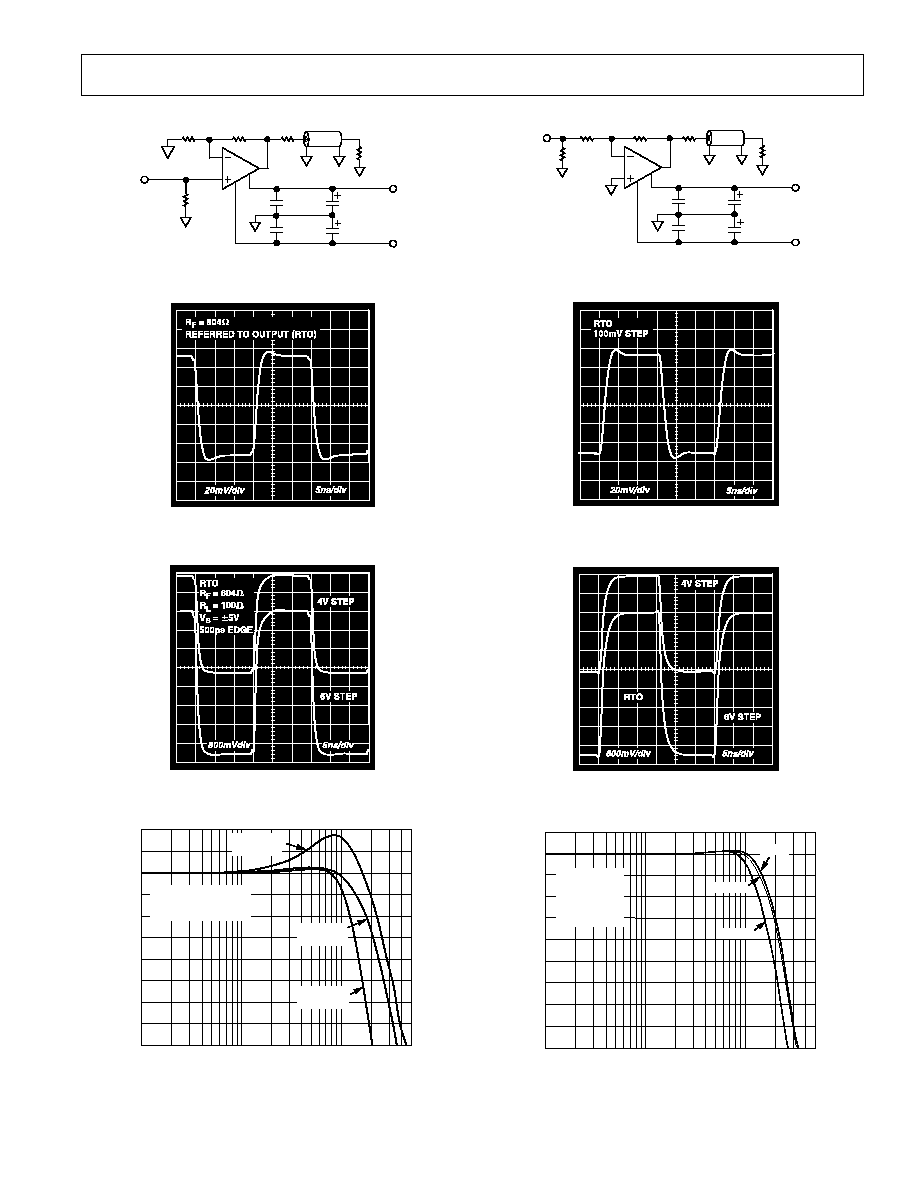
61.9
0.1 F
0.1 F
10 F
10 F
499
249
V
IN
+V
S
V
S
50
SCOPE
INPUT
50
Figure 8. Test Circuit; Gain = 2
Figure 9.* 100 mV Step Response; G = 2, V
S
=
±
2.5 V or
±
5 V
Figure 10.* Step Response; G = 2, V
S
=
±
5 V
FREQUENCY MHz
+1
NORMALIZED FREQUENCY RESPONSE dB
4
9
1
500
10
40
100
3
2
1
0
5
6
7
8
G = 1
G = 2
G = 10
V
S
= 5V
R
F
= 499
V
IN
= 50mV rms
R
L
= 100
N PACKAGE
Figure 11. Frequency Response, G = 1, 2, 10
0.1 F
0.1 F
10 F
10 F
604
604
50
V
IN
+V
S
V
S
50
SCOPE
INPUT
50
Figure 4. Test Circuit; Gain = +2
Figure 5.* 100 mV Step Response; G = +2, V
S
=
±
2.5 V or
±
5 V
Figure 6.* Step Response; G = +2, V
S
=
±
5 V
FREQUENCY MHz
+2
3
8
1
500
10
NORMALIZED FREQUENCY RESPONSE dB
40
100
2
1
0
+1
4
5
6
7
G = +2,
R
F
= 604
G = +10,
R
F
= 499
R
L
= 100
V
IN
= 50mV (G = +1, +2)
V
IN
= 5mV (G = +10)
G = +1,
R
F
= 698
Figure 7. Frequency Response; G = +1, +2, +10, V
S
=
±
5 V
*NOTE: V
S
=
±
2.5 V operation is identical to V
S
= +5 V single supply operation.
REV. B
AD8004
6
FREQUENCY MHz
+9
6
21
1
500
10
OUTPUT LEVEL dBV
40
100
3
0
+3
+6
9
12
15
18
1V rms
G =+2
V
S
= 5V
R
F
= 604
Figure 12. Large Signal Frequency Response; V
S
=
±
5.0 V,
G = +2, R
F
= 604
FREQUENCY MHz
50
100
1
20
DISTORTION dBc
10
40
60
70
80
90
G = +2
V
O
= 2V p-p
R
F
= 698
2ND
R
L
= 150
3RD
R
L
= 150
2ND
R
L
= 1k
3RD
R
L
= 1k
Figure 13. Distortion vs. Frequency; V
S
=
±
5 V
FREQUENCY MHz
+1
4
9
1
500
10
40
100
3
2
1
0
5
6
7
8
NORMALIZED FREQUENCY RESPONSE dB
NORMALIZED FLATNESS dB
+0.1
0
0.1
0.2
0.3
0.4
0.5
G = +2
V
IN
= 50mV rms
R
L
= 100
R
F
= 1.10k
R PACKAGE
5V
S
+5V
S
+5V
S
5V
S
Figure 14. Frequency Response and Flatness, G = +2
FREQUENCY MHz
+3
12
27
1
500
10
40
100
9
6
3
0
15
18
21
24
1V rms
OUTPUT LEVEL dBV
G = +2
V
S
= +5V
R
F
= 604
Figure 15. Large Signal Frequency Response; V
S
= +5.0 V,
G = +2, R
F
= 604
FREQUENCY MHz
40
70
100
1
20
DISTORTION dBc
10
60
50
80
90
G = +2
V
O
= 2V p-p
R
F
= 698
2ND
R
L
= 150
3RD
R
L
= 150
2ND
R
L
= 1k
3RD
R
L
= 1k
Figure 16. Distortion vs. Frequency; V
S
= +5 V
CMRR dB
604
604
50
V
OUT
154
154
57.6
V
IN
FREQUENCY MHz
10
35
60
0.1
500
1
10
100
30
25
20
15
40
45
50
55
+5V
S
5V
S
+5V
S
5V
S
0.03
Figure 17. CMRR vs. Frequency; V
S
=
±
5 V or +5 V,
V
IN
= 200 mV rms, Other Sides Are Equal, RTO
REV. B
AD8004
7
INPUT CURRENT NOISE pA/
Hz
9
10 100 1k 10k 100k 1M
FREQUENCY Hz
1000
500
200
100
300
10
8
7
6
5
4
3
2
10
9
8
7
6
5
4
3
2
1
70
50
40
30
20
+ OR INPUT
CURRENT NOISE
VOLTAGE NOISE
INPUT VOLTAGE NOISE nV/
Hz
10
Figure 18. Noise vs. Frequency, V
S
= +5 V or
±
5 V
S
FREQUENCY MHz
1
0.1
500
1
IMPEDANCE
10
100
10
100
0.1
0.01
0.03
+5V
S
5V
S
R
bT
= 50
5V
S
OR +5V
S
R
bT
= 0
G = +2
R
F
= 698
POWER = 0dBm
(224mV rms)
Figure 19. Output Impedance vs. Frequency
FREQUENCY MHz
180
0.1
500
1
10
100
90
0
240
360
0.03
+60
+50
+40
+30
+20
+10
PHASE Degrees
0
10
GAIN dB
V
IN
= 40dBm
V
S
= 5V
GAIN
PHASE
Figure 20. Open-Loop Voltage Gain and Phase
PSRR dB
FREQUENCY Hz
0
50
10k
500M
100k
1M
10M
40
30
20
10
60
70
80
100M
+PSRR
PSRR
G = +2
5V
S
OR 2.5V
S
R
F
= 1k
100mV rms ON TOP
OF dc BIAS
Figure 21. PSRR vs. Frequency
FREQUENCY MHz
CROSSTALK dB
20
70
120
0.1
500
1
10
100
60
50
40
30
80
90
100
110
0.03
OUTPUT =
SIDE 2
OUTPUT =
SIDE 4
OUTPUT =
SIDE 3
G = +2
R
F
= 1.10k
5V
S
V
IN
= 200mV rms
INPUT TO SIDE 1
R
L1
= 1k
R PACKAGE
Figure 22. Crosstalk (Output to Output) vs. Frequency
FREQUENCY Hz
GAIN dB
110
60
10
1M
1G
10M
100M
70
80
90
100
50
40
30
20
100k
PHASE
GAIN
0
50
100
150
200
PHASE Degree
Figure 23. Open-Loop Transimpedance Gain
REV. B
AD8004
8
Figure 24. Short-Term Settling Time
Figure 25. Long-Term Settling Time
0.04
0.03
0.02
0.01
0.00
0.01
0.02
0.03
0.04
1
ST
DIFF GAIN %
0.12
0.10
0.08
0.06
0.04
0.02
0.00
0.02
0.04
DIFF PHASE Degrees
2
ND
3
RD
4
TH
5
TH
6
TH
7
TH
8
TH
9
TH
10
TH
11
TH
80 IRE
R
L
= 150
V
S
= 5V
R
F
= 1.21k
80 IRE
R
L
= 150
V
S
= 5V
R
F
= 1.21k
1
ST
2
ND
3
RD
4
TH
5
TH
6
TH
7
TH
8
TH
9
TH
10
TH
11
TH
Figure 26. Differential Gain/Differential Phase
9
8
7
6
5
3
2
10 100 1000 10000
LOAD RESISTANCE
4
1
0
SWING V p
-
p
+5V
S
5V
S
G = +2
R
F
= 1.21k
Figure 27. Output Voltage Swing vs. Load
9
8
7
6
5
4
3
2
1
0
R
L
= 100
R
L
= 1k
TOTAL SUPPLY VOLTAGE V
G = +2
R
F
= 1.21k
f = 100kHz
10
3
4
5
6
7
8
9
10
11
12
PEAK-TO-PEAK OUTPUT
AT CLIPPING POINT V
Figure 28. Output Swing vs. Supply
0.03
0.02
0.01
0.00
0.01
0.02
0.03
DIFF GAIN %
DIFF PHASE Degrees
80 IRE
R
L
= 1k
V
S
= 5V
R
F
= 1.21k
0.04
0.03
0.02
0.01
0.00
0.01
0.02
0.03
0.04
1
ST
2
ND
3
RD
4
TH
5
TH
6
TH
7
TH
8
TH
9
TH
10
TH
11
TH
1
ST
2
ND
3
RD
4
TH
5
TH
6
TH
7
TH
8
TH
9
TH
10
TH
11
TH
80 IRE
R
L
= 1k
V
S
= 5V
R
F
= 1.21k
Figure 29. Differential Gain/Phase, R
L
= 1 k
REV. B
AD8004
9
THEORY OF OPERATION
The AD8004 is a member of a new family of high speed current-
feedback (CF) amplifiers offering new levels of bandwidth,
distortion, and signal-swing capability vs. power. Its wide dynamic
range capabilities are due to both a complementary high speed
bipolar process and a new design architecture. The AD8004 is
basically a two stage (Figure 30) rather than the conventional
one stage design. Both stages feature the current-on-demand
property associated with current feedback amplifiers. This gives
an unprecedented ratio of quiescent current to dynamic perfor-
mance. The important properties of slew rate, and full power
bandwidth benefit from this performance. In addition the
second gain stage buffers the effects of load impedance sig-
nificantly reducing distortion.
A full discussion of this new amplifier architecture is available on
the data sheet for the AD8011. This discussion only covers the
basic principles of operation.
DC AND AC CHARACTERISTICS
As with traditional op amp circuits the dc closed-loop gain is
defined as:
A
V
=
G
=
1
+
R
F
R
N
noninverting operation
A
V
=
G
= -
R
F
R
N
inverting operation
The more exact relationships that take into account open-loop
gain errors are:
A
V
=
G
1
+
1
-
G
A
O
(
s)
+
R
F
T
O
(
s)
for inverting (G is negative)
A
V
=
G
1
+
G
A
O
(
s)
+
R
F
T
O
(
s)
for noninverting (G is positive)
In these equations the open-loop voltage gain (A
O
(s)) is com-
mon to both voltage and current-feedback amplifiers and is the
ratio of output voltage to differential input voltage. The open-
loop transimpedance gain (T
O
(s)) is the ratio of output voltage
to inverting input current and is applicable to current-feedback
amplifiers. The open-loop voltage gain and open-loop transim-
pedance gain (T
O
(s)) of the AD8004 are plotted vs. frequency
in Figures 20 and 23. These plots and the basic relationships
can be used to predict the first order performance of the AD8004
over frequency. At low closed-loop gains the term (R
F
/T
O
(s))
dominates the frequency response characteristics. This gives the
result that bandwidth is constant with gain, a familiar property
of current feedback amplifiers.
An R
F
of 1 k
has been chosen as the nominal value to give
optimum frequency response with acceptable peaking at gains of
+2/1. As can be seen from the above relationships, at higher
closed-loop gains reducing R
F
has the effect of increasing closed-
loop bandwidth. Table I gives optimum values for R
F
and R
G
for a variety of gains.
V
P
Q1
Q2
IPP
IPN
INP
IPN
V
N
Z
I
IQ1
Q3
Q4
IE
C
P
1
C
P
1
A2
C
L
R
G
R
F
V
O
C
D
ICQ +
IO
V
O
´
IQ1
AD8004
A2
C
P
2
C
D
A3
R
L
A1
A1
Z2
Figure 30. Simplified Block Diagram
REV. B
AD8004
10
DRIVING CAPACITIVE LOADS
The AD8004 was designed primarily to drive nonreactive loads.
If driving loads with a capacitive component is desired, best
settling response is obtained by the addition of a small series
resistance as shown in Figure 31. The accompanying graph
shows the optimum value for R
SERIES
vs. capacitive load. It is
worth noting that the frequency response of the circuit when
driving large capacitive loads will be dominated by the passive
roll-off of R
SERIES
and C
L
.
1k
R
L
1k
C
L
AD8004
R
SERIES
1k
Figure 31. Driving Capacitive Load
40
30
20
0
10
15
20
25
C
L
pF
10
R
SERIES
5
Figure 32. Recommended R
SERIES
vs. Capacitive Load for
30 ns Settling to 0.1%
OPTIMIZING FLATNESS
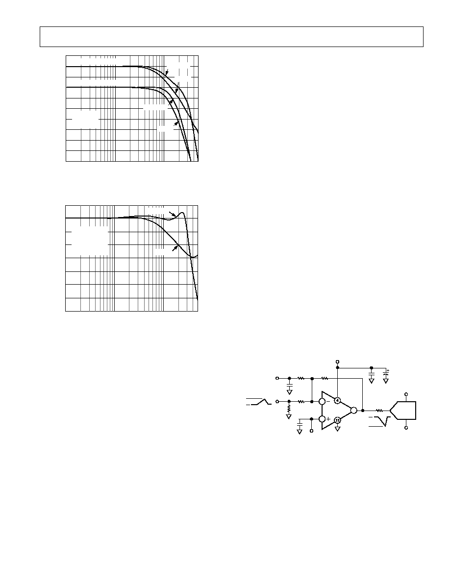
The fine scale gain flatness and 3 dB bandwidth is affected by
R
FEEDBACK
selection as is normal of current feedback amplifiers.
With exception of gain = +1, the AD8004 can be adjusted for
either maximal flatness with modest closed-loop bandwidth or
for mildly peaked-up frequency response with much more band-
width. Figure 33 shows the effect of three evenly spaced R
F
changes upon gain = +1 and gain = +2. Table I shows the
recommended component values for achieving maximally flat
frequency response as well as a faster slightly peaked-up fre-
quency response.
Printed circuit board parasitics and device lead frame parasitics
also control fine scale gain flatness. The AD8004R package
because of its small lead frame offers superior parasitics relative
to the N package. In the printed circuit board environment,
parasitics such as extra capacitance caused by two parallel and
vertical flat conductors on opposite PC board sides in the
region of the summing junction will cause some bandwidth
extension and/or increased peaking. In noninverting gains, the
effect of extra capacitance on summing junctions is far more
pronounced than versus inverting gains. Figure 34 shows an
example of this. Note that only 1 pF of added junction capaci-
tance causes about a 70% bandwidth extension and additional
peaking on a gain = +2. For an inverting gain = 2, 5 pF of
additional summing junction capacitance caused a small 10%
bandwidth extension.
Extra output capacitive loading also causes bandwidth exten-
sions and peaking. The effect is more pronounced with less
resistive loading from the next stage. Figure 35 shows the effect
of direct output capacitive loads for gains of +2 and 2. For both
gains C
LOAD
was set to 10 pF or 0 pF (no extra capacitive loading).
For each of the four traces in Figure 35 the resistive loads were
100
. Figure 36 also shows capacitive loading effects only
with a lighter output resistive load. Note that even though
bandwidth is extended 2
×
, the flatness dramatically suffers.
FREQUENCY MHz
2
1
500
10
40
100
+1
0
1
V
IN
= 50mV rms
V
S
= 5V
R
L
= 100
R PACKAGE
3
4
5
NORMALIZED GAIN dB, G = +2
+2
3
0
+1
1
2
4
5
6
R
F
= 1.10k
R
F
= 604
G = +1
G = +2
7
8
GAIN dB, G = +1
R
F
= 845
R
F
= 909
R
F
= 1.1k
R
F
= 698
Figure 33. R
FEEDBACK
vs. Frequency Response, G = +1/+2
FREQUENCY MHz
+2
8
1
500
10
40
100
2
0
4
6
V
IN
= 50mV rms
R
L
= 100
5V
S
10
12
14
NORMALIZED GAIN dB, G = 2
NORMALIZED GAIN dB, G = +2
+2
8
2
0
4
6
10
12
14
C
J
= 1pF
C
J
= 0
C
J
= 5.1pF
C
J
= 0
G = +2
G = 2
Figure 34. Frequency Response vs. Added Summing
Junction Capacitance
REV. B
AD8004
11
FREQUENCY MHz
+2
8
1
500
10
40
100
2
0
4
6
V
IN
= 50mV
5V
S
R
L
= 100
10
12
14
NORMALIZED GAIN dB, G = 2
NORMALIZED GAIN dB
,
G = +2
+2
8
2
0
4
6
10
12
14
C
L
= 10pF
C
L
= 0
C
L
= 10pF
C
L
= 0
G = +2, R
F
= 1.10k
G = 2, R
F
= 698
Figure 35. Frequency Response vs. Capacitive Loading,
R
L
= 100
Output
FREQUENCY MHz
+2
8
1
500
10
40
100
2
0
4
6
10
12
14
NORMALIZED GAIN dB, G = 2
C
L
= 10pF
C
L
= 0
G = +2
R
L
= 1k
5V
S
V
IN
= 50mV rms
R
F
= 1.2k
Figure 36. Flatness with 10 pF Capacitive Load
DRIVING A SINGLE-SUPPLY A/D CONVERTER
New CMOS A/D converters are placing greater demands on the
amplifiers that drive them. Higher resolutions, faster conversion
rates and input switching irregularities require superior settling
characteristics. In addition, these devices run off a single +5 V
supply and consume little power, so good single-supply operation
with low power consumption are very important. The AD8004
is well positioned for driving this new class of A/D converters.
Figure 37 shows a circuit that uses an AD8004 to drive an
AD876, a single supply, 10-bit, 20 MSPS A/D converter that
requires only 140 mW. Using the AD8004 for level shifting and
driving, the A/D exhibits no degradation in performance com-
pared to when it is driven from a signal generator.
The analog input of the AD876 spans 2 V centered at about
2.6 V. The resistor network and bias voltages provide the level
shifting and gain required to convert the 0 V to 1 V input signal
to a 3.6 V to 1.6 V range that the AD876 wants to see.
Biasing the noninverting input of the AD8004 at 1.6 V dc forces
the inverting input to be at 1.6 V dc for linear operation of the
amplifier. When the input is at 0 V, there is 3.2 mA flowing out
of the summing junction via R1 (1.6 V/499
). R3 has a current
of 1.2 mA flowing into the summing junction (3.6 V1.6 V)/
1.65 k
. The difference of these two currents (2 mA) must flow
through R2. This current flows toward the summing junction
and requires that the output be 2 V higher than the summing
junction or at 3.6 V.
When the input is at 1 V, there is 1.2 mA flowing into the sum-
ming junction through R3 and 1.2 mA flowing out through R1.
These currents balance and leave no current to flow through
R2. Thus the output is at the same potential as the inverting
input or 1.6 V.
The input of the AD876 has a series MOSFET switch that turns
on and off at the sampling rate. This MOSFET is connected to
a hold capacitor internal to the device. The on impedance of the
MOSFET is about 50
, while the hold capacitor is about 5 pF.
In a worst case condition, the input voltage to the AD876 will
change by a full-scale value (2 V) in one sampling cycle. When
the input MOSFET turns on, the output of the op amp will be
connected to the charged hold capacitor through the series
resistance of the MOSFET. Without any other series resistance,
the instantaneous current that flows would be 40 mA. This
would cause settling problems for the op amp.
The series 100
resistor limits the current that flows instanta-
neously after the MOSFET turns on to about 13 mA. This
resistor cannot be made too large or the high frequency perfor-
mance will be affected.
The sampling MOSFET of the AD876 is closed for only half of
each cycle or for 25 ns. Approximately seven time constants are
required for settling to 10 bits. The series 100
resistor along
with the 50
on resistance and the hold capacitor, create a
750 ps time constant. These values leave a comfortable margin
for settling. Obtaining the same results with the op amp A/D
combination as compared to driving with a signal generator
indicates that the op amp is settling fast enough.
Overall the AD8004 provides adequate buffering for the AD876
A/D converter without introducing distortion greater than that
of the A/D converter by itself.
3.6V
1.6V
+5V
10 F
R2
1k
R3
1.65k
R1
499k
3.6V
V
IN
50
0.1 F
1.6V
1V
0V
100
+1.6V
+3.6V
REFT
REFB
0.1 F
0.1 F
1/4
AD8004
AD876
Figure 37. AD8004 Driving the AD876
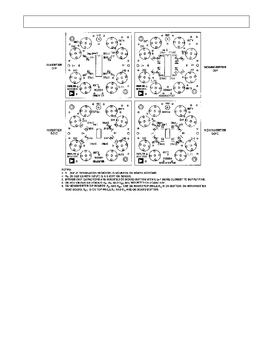
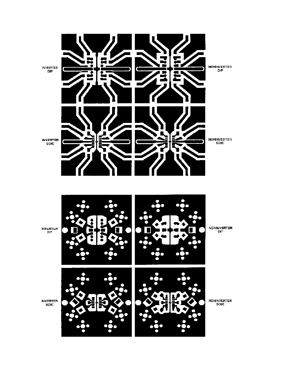
LAYOUT CONSIDERATIONS
The specified high speed performance of the AD8004 requires
careful attention to board layout and component selection.
Table I shows the recommended component values for the
AD8004 and Figures 3941 show the layout for the AD8004
evaluation boards (14-lead DIP and SOIC). Proper R
F
design
techniques and low parasitic component selection are mandatory.
REV. B
AD8004
12
Table I. Recommended Component Values and Typical Bandwidths
Alternate
Alternate
Alternate
Alternate
Gain
10
2
2
1
1
+1
+1
+2
+2
+10
AD8004AN (DIP)
PACKAGE TYPE
R
F
(
)
499
698
499
649
499
1.21 k
806
1.10 k
698
499
R
G
(
)
49.9
348
249
649
499
1.10 k
698
54.9
R
T
(
)
None
57.6
61.9
53.6
54.9
50
50
50
50
50
Small Signal BW
@
±
5 V
S
(MHz)
155
125
180
135
190
150
250
115
185
135
Peaking @
±
5 V
S
< 0.3 dB
None
0.3 dB
None
0.3 dB
1.3 dB
1.7 dB
< 0.14 dB
0.4 dB
< 0.3 dB
0.1 dB Flatness
@
±
5 V
S
(MHz)
25
30
35
Small Signal BW
@ +5 V
S
(MHz)
135
105
155
120
160
130
200
95
150
120
AD8004AR (SOIC)
PACKAGE TYPE
R
F
(
)
499
698
499
750
499
1.10 k
698
1.10 k
604
499
R
G
(
)
49.9
348
249
750
499
1.10 k
604
54.9
R
T
(
)
None
57.6
61.9
53.6
54.9
50
50
50
50
50
Small Signal BW
@
±
5 V
S
(MHz)
155
130
190
125
195
150
225
110
175
135
Peaking @
±
5 V
S
< 0.7 dB
< 0.1 dB
0.5 dB
None
0.4 dB
1.3 dB
1.8 dB
< 0.1 dB
0.5 dB
< 0.2 dB
0.1 dB Flatness
@
±
5 V
S
(MHz)
35
25
30
Small Signal BW
@ +5 V
S
(MHz)
135
115
175
110
165
130
195
95
155
120
NOTES
1
R
T
chosen for 50
characteristic input impedance.
2
Resistor values listed are standard 1% tolerance.
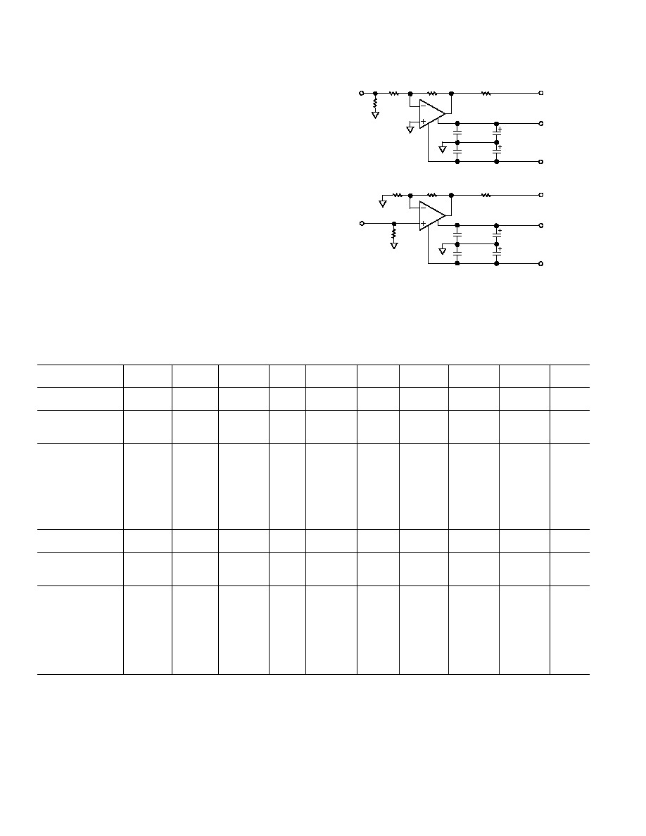
The PCB should have a ground plane covering all unused por-
tions of the component side of the board to provide a low im-
pedance ground path. The ground plane should be removed
from the area near the input pins to reduce stray capacitance.
Chip capacitors should be used for supply bypassing (see
Figure 38). One end should be connected to the ground plane
and the other within 1/8 in. of each power pin. An additional
(4.7
µ
F10
µ
F) tantalum electrolytic capacitor should be con-
nected in parallel.
The feedback resistor should be located close to the inverting
input pin in order to keep the stray capacitance at this node to a
minimum. Capacitance greater than 1 pF at the inverting input
will significantly affect high speed performance when operating
at low noninverting gains. An example of extra inverting input
capacitance can be seen on Figure 35 plot.
Stripline design techniques should be used for long signal traces
(greater than about 1 in.). These should be designed with the
proper system characteristic impedance and be properly termi-
nated at each end.
NONINVERTING CONFIGURATION
C1
0.1 F
C2
0.1 F
C4
10 F
C3
10 F
R
T
V
IN
V
OUT
+V
S
V
S
R
G
R
F
R
bT
, 50
1/4
C1
0.1 F
C2
0.1 F
C4
10 F
C3
10 F
R
T
V
IN
V
OUT
+V
S
V
S
R
G
R
F
R
bT
, 50
1/4
INVERTING CONFIGURATION
Figure 38. Inverting and Noninverting Configurations
REV. B
AD8004
13
Figure 39. Evaluation Board Silkscreen (Top)
REV. B
AD8004
14
Figure 40 Evaluation Board Layout (Top Side)
Figure 41. Evaluation Board Layout (Bottom Side, Looking Through the Board)
REV. B
AD8004
15
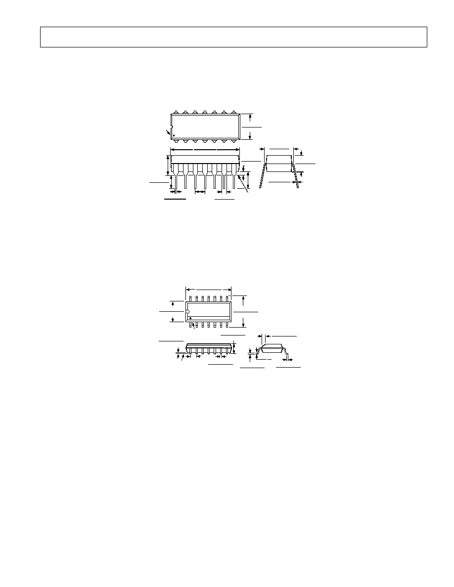
OUTLINE DIMENSIONS
Dimensions shown in inches and (mm).
14-Lead Plastic DIP
(N-14)
0.210
(5.33)
MAX
0.160 (4.06)
0.115 (2.93)
0.795 (20.19)
0.725 (18.42)
0.022 (0.558)
0.014 (0.356)
0.100
(2.54)
BSC
PIN 1
0.280 (7.11)
0.240 (6.10)
0.325 (8.25)
0.300 (7.62)
0.015 (0.381)
0.008 (0.204)
0.195 (4.95)
0.115 (2.93)
0.070 (1.77)
0.045 (1.15)
SEATING
PLANE
0.060 (1.52)
0.015 (0.38)
0.130
(3.30)
MIN
7
8
14
1
14-Lead Plastic SOIC
(R-14)
14
8
7
1
0.3444 (8.75)
0.3367 (8.55)
0.2440 (6.20)
0.2284 (5.80)
0.1574 (4.00)
0.1497 (3.80)
PIN 1
SEATING
PLANE
0.0098 (0.25)
0.0040 (0.10)
0.0192 (0.49)
0.0138 (0.35)
0.0688 (1.75)
0.0532 (1.35)
0.0500
(1.27)
BSC
0.0099 (0.25)
0.0075 (0.19)
0.0500 (1.27)
0.0160 (0.41)
8
°
0
°
0.0196 (0.50)
0.0099 (0.25)
x 45
°
C2078a08/99
PRINTED IN U.S.A.

16
C2078a08/99
PRINTED IN U.S.A.