Äîêóìåíòàöèÿ è îïèñàíèÿ www.docs.chipfind.ru
REV. A
Information furnished by Analog Devices is believed to be accurate and
reliable. However, no responsibility is assumed by Analog Devices for its
use, nor for any infringements of patents or other rights of third parties
which may result from its use. No license is granted by implication or
otherwise under any patent or patent rights of Analog Devices.
a
AD8005
One Technology Way, P.O. Box 9106, Norwood, MA 02062-9106, U.S.A.
Tel: 781/329-4700
World Wide Web Site: http://www.analog.com
Fax: 781/326-8703
© Analog Devices, Inc., 1999
FEATURES
Ultralow Power
400
A Power Supply Current (4 mW on 5 V
S
)
Specified for Single Supply Operation
High Speed
270 MHz, 3 dB Bandwidth (G = +1)
170 MHz, 3 dB Bandwidth (G = +2)
280 V/ s Slew Rate (G = +2)
28 ns Settling Time to 0.1%, 2 V Step (G = +2)
Low Distortion/Noise
63 dBc @ 1 MHz, V
O
= 2 V p-p
50 dBc @ 10 MHz, V
O
= 2 V p-p
4.0 nV/
Hz Input Voltage Noise @ 10 MHz
Good Video Specifications (R
L
= 1 k , G = +2)
Gain Flatness 0.1 dB to 30 MHz
0.11% Differential Gain Error
0.4 Differential Phase Error
APPLICATIONS
Signal Conditioning
A/D Buffer
Power-Sensitive, High-Speed Systems
Battery Powered Equipment
Loop/Remote Power Systems
Communication or Video Test Systems
Portable Medical Instruments
FUNCTIONAL BLOCK DIAGRAM
8-Lead Plastic DIP and SOIC
1
2
3
4
8
7
6
5
AD8005
NC
IN
+IN
V
S
NC
+V
S
OUT
NC
NC = NO CONNECT
5-Lead SOT-23
4
5
1
2
3
AD8005
V
S
+V
S
IN
OUT
+IN
PRODUCT DESCRIPTION
The AD8005 is an ultralow power, high-speed amplifier with a
wide signal bandwidth of 170 MHz and slew rate of 280 V/
µ
s.
This performance is achieved while consuming only 400
µ
A of
quiescent supply current. These features increase the operating
time of high-speed battery-powered systems without reducing
dynamic performance.
FREQUENCY MHz
0.1
500
10
100
0
3
2
1
1
2
3
4
5
6
V
S
= ±5V
1
V
S
= +5V
NORMALIZED GAIN dB
G = +2
V
OUT
= 200mV p-p
R
L
= 1k
Figure 1. Frequency Response; G = +2, V
S
= +5 V or
±
5 V
270 MHz, 400 A
Current Feedback Amplifier
The current feedback design results in gain flatness of 0.1 dB
to 30 MHz while offering differential gain and phase errors of
0.11% and 0.4
°
. Harmonic distortion is low over a wide
bandwidth with THDs of 63 dBc at 1 MHz and 50 dBc at
10 MHz. Ideal features for a signal conditioning amplifier or
buffer to a high-speed A-to-D converter in portable video,
medical or communication systems.
The AD8005 is characterized for +5 V and
±
5 V supplies and
will operate over the industrial temperature range of 40
°
C to
+85
°
C. The amplifier is supplied in 8-lead plastic DIP, 8-lead
SOIC and 5-lead SOT-23 packages.
FREQUENCY MHz
20
10
40
60
80
100
50
70
90
3RD
1
2ND
DISTORTION dBc
G = +2
V
OUT
= 2V p-p
R
L
= 1k
3RD
2ND
Figure 2. Distortion vs. Frequency; V
S
=
±
5 V

AD8005SPECIFICATIONS
2
REV. A
5 V SUPPLIES
AD8005A
Parameter
Conditions
Min
Typ
Max
Units
DYNAMIC PERFORMANCE
R
F
= 3.01 k
for "N" Package or
R
F
= 2.49 k
for "R" Package or
R
F
= 2.10 k
for "RT" Package
3 dB Small Signal Bandwidth
G = +1, V
O
= 0.2 V p-p
225
270
MHz
G = +2, V
O
= 0.2 V
p-p
140
170
MHz
Bandwidth for 0.1 dB Flatness
G = +2, V
O
= 0.2 V
p-p
10
30
MHz
Large Signal Bandwidth
G = +10, V
O
= 4 V p-p, R
F
= 499
40
MHz
Slew Rate (Rising Edge)
G = +2, V
O
= 4 V Step
280
V/
µ
s
G = 1, V
O
= 4 V Step, R
F
= 1.5 k
1500
V/
µ
s
Settling Time to 0.1%
G = +2, V
O
= 2 V Step
28
ns
DISTORTION/NOISE PERFORMANCE
R
F
= 3.01 k
for "N" Package or
R
F
= 2.49 k
for "R" Package or
R
F
= 2.10 k
for "RT" Package
Total Harmonic Distortion
f
C
= 1 MHz, V
O
=
2 V p-p, G = +2
63
dBc
f
C
= 10 MHz, V
O
=
2 V p-p, G = +2
50
dBc
Differential Gain
NTSC, G = +2
0.11
%
Differential Phase
NTSC, G = +2
0.4
Degrees
Input Voltage Noise
f = 10 MHz
4.0
nV/
Hz
Input Current Noise
f = 10 MHz, +I
IN
1.1
pA/
Hz
I
IN
9.1
pA/
Hz
DC PERFORMANCE
Input Offset Voltage
5
30
±
mV
T
MIN
to T
MAX
50
±
mV
Offset Drift
40
µ
V/
°
C
+Input Bias Current
0.5
1
±µ
A
T
MIN
to T
MAX
2
±µ
A
Input Bias Current
5
10
±µ
A
T
MIN
to T
MAX
12
±µ
A
Input Bias Current Drift (
±
)
6
nA/
°
C
Open-Loop Transimpedance
400
1000
k
INPUT CHARACTERISTICS
Input Resistance
+Input
90
M
Input
260
Input Capacitance
+Input
1.6
pF
Input Common-Mode Voltage Range
3.8
±
V
Common-Mode Rejection Ratio
V
CM
=
±
2.5 V
46
54
dB
OUTPUT CHARACTERISTICS
Output Voltage Swing
Positive
+3.7
+3.90
V
Negative
3.90
3.7
V
Output Current
R
L
= 50
10
mA
Short Circuit Current
60
mA
POWER SUPPLY
Quiescent Current
400
475
µ
A
T
MIN
to T
MAX
560
µ
A
Power Supply Rejection Ratio
V
S
=
±
4 V to
±
6 V
56
66
dB
OPERATING TEMPERATURE RANGE
40
+85
°
C
Specifications subject to change without notice.
(@ T
A
= +25 C, V
S
= 5 V, R
L
= 1 k
unless otherwise noted)

+5 V SUPPLY
AD8005A
Parameter
Conditions
Min
Typ
Max
Units
DYNAMIC PERFORMANCE
R
F
= 3.01 k
for "N" Package or
R
F
= 2.49 k
for "R" Package or
R
F
= 2.10 k
for "RT" Package
3 dB Small Signal Bandwidth
G = +1, V
O
= 0.2 V p-p
190
225
MHz
G = +2, V
O
= 0.2 V p-p
110
130
MHz
Bandwidth for 0.1 dB Flatness
G = +2, V
O
= 0.2 V p-p
10
30
MHz
Large Signal Bandwidth
G = +10, V
O
= 2 V p-p, R
F
= 499
45
MHz
Slew Rate (Rising Edge)
G = +2, V
O
= 2 V Step
260
V/
µ
s
G = 1, V
O
= 2 V Step, R
F
= 1.5 k
775
V/
µ
s
Settling Time to 0.1%
G = +2, V
O
= 2 V Step
30
ns
DISTORTION/NOISE PERFORMANCE
R
F
= 3.01 k
for "N" Package or
R
F
= 2.49 k
for "R" Package or
R
F
= 2.10 k
for "RT" Package
Total Harmonic Distortion
f
C
= 1 MHz, V
O
= 2 V p-p, G = +2
60
dBc
f
C
= 10 MHz, V
O
= 2 V p-p, G = +2
50
dBc
Differential Gain
NTSC, G = +2, R
L
to 1.5 V
0.14
%
Differential Phase
NTSC, G = +2, R
L
to 1.5 V
0.70
Degrees
Input Voltage Noise
f = 10 MHz
4.0
nV/
Hz
Input Current Noise
f = 10 MHz, +I
IN
1.1
pA/
Hz
I
IN
9.1
pA/
Hz
DC PERFORMANCE
Input Offset Voltage
5
35
±
mV
T
MIN
to T
MAX
50
±
mV
Offset Drift
40
µ
V/
°
C
+Input Bias Current
0.5
1
±µ
A
T
MIN
to T
MAX
2
±µ
A
Input Bias Current
5
10
±µ
A
T
MIN
to T
MAX
11
±µ
A
Input Bias Current Drift (
±
)
8
nA/
°
C
Open-Loop Transimpedance
50
500
k
INPUT CHARACTERISTICS
Input Resistance
+Input
120
M
Input
300
Input Capacitance
+Input
1.6
pF
Input Common-Mode Voltage Range
1.5 to 3.5
V
Common-Mode Rejection Ratio
V
CM
= 1.5 V to 3.5 V
48
54
dB
OUTPUT CHARACTERISTICS
Output Voltage Swing
1.1 to 3.9
0.95 to 4.05
V
Output Current
R
L
= 50
10
mA
Short Circuit Current
30
mA
POWER SUPPLY
Quiescent Current
350
425
µ
A
T
MIN
to T
MAX
475
µ
A
Power Supply Rejection Ratio
V
S
= +4 V to +6 V
56
66
dB
OPERATING TEMPERATURE RANGE
40
+85
°
C
Specifications subject to change without notice.
(@ T
A
= +25 C, V
S
= +5 V, R
L
= 1 k
to 2.5 V unless otherwise noted)
AD8005
3
REV. A
AD8005
4
REV. A
ABSOLUTE MAXIMUM RATINGS
1
Supply Voltage . . . . . . . . . . . . . . . . . . . . . . . . . . . . . . . . 12.6 V
Internal Power Dissipation
2
Plastic DIP Package (N) . . . . . . . . . . . . . . . . . . . . 1.3 Watts
Small Outline Package (R) . . . . . . . . . . . . . . . . . . 0.75 Watts
SOT-23-5 Package (RT) . . . . . . . . . . . . . . . . . . . 0.5 Watts
Input Voltage (Common Mode) . . . . . . . . . . . . . . .
±
V
S
±
1 V
Differential Input Voltage . . . . . . . . . . . . . . . . . . . . . . .
±
3.5 V
Output Short Circuit Duration
. . . . . . . . . . . . . . . . . . . . . . . Observe Power Derating Curves
Storage Temperature Range
N, R & RT Package . . . . . . . . . . . . . . . . . 65
°
C to +125
°
C
Operating Temperature Range (A Grade) . . . 40
°
C to +85
°
C
Lead Temperature Range (Soldering 10 sec) . . . . . . . . +300
°
C
NOTES
1
Stresses above those listed under Absolute Maximum Ratings may cause perma-
nent damage to the device. This is a stress rating only; functional operation of the
device at these or any other conditions above those indicated in the operational
section of this specification is not implied. Exposure to absolute maximum rating
conditions for extended periods may affect device reliability.
2
Specification is for device in free air:
8-Lead Plastic DIP Package:
JA
= 90
°
C/W
8-Lead SOIC Package:
JA
= 155
°
C/W
5-Lead SOT-23 Package:
JA
= 240
°
C/W
CAUTION
ESD (electrostatic discharge) sensitive device. Electrostatic charges as high as 4000 V readily
accumulate on the human body and test equipment and can discharge without detection.
Although the AD8005 features proprietary ESD protection circuitry, permanent damage may
occur on devices subjected to high-energy electrostatic discharges. Therefore, proper ESD
precautions are recommended to avoid performance degradation or loss of functionality.
MAXIMUM POWER DISSIPATION
The maximum power that can be safely dissipated by the
AD8005 is limited by the associated rise in junction tempera-
ture. The maximum safe junction temperature for plastic
encapsulated devices is determined by the glass transition tem-
perature of the plastic, approximately +150
°
C. Exceeding this
limit temporarily may cause a shift in parametric performance
due to a change in the stresses exerted on the die by the package.
Exceeding a junction temperature of +175
°
C for an extended
period can result in device failure.
While the AD8005 is internally short circuit protected, this may
not be sufficient to guarantee that the maximum junction tem-
perature (+150
°
C) is not exceeded under all conditions. To
ensure proper operation, it is necessary to observe the maximum
power derating curves shown in Figure 3.
AMBIENT TEMPERATURE °C
90
80
2.0
1.0
0
1.5
0.5
8-LEAD PLASTIC-DIP PACKAGE
50
T
J
= +150°C
MAXIMUM POWER DISSIPATION Watts
70
60
50
40
30
20
10
0
40 30 20 10
8-LEAD SOIC PACKAGE
5-LEAD SOT-23 PACKAGE
Figure 3. Maximum Power Dissipation vs. Temperature
WARNING!
ESD SENSITIVE DEVICE
ORDERING GUIDE
Temperature
Package
Package
Brand
Model
Range
Description
Option
Code
AD8005AN
40
°
C to +85
°
C
8-Lead Plastic DIP
N-8
AD8005AR
40
°
C to +85
°
C
8-Lead Plastic SOIC
SO-8
AD8005AR-REEL
40
°
C to +85
°
C
13" Tape and Reel
SO-8
AD8005ART-REEL
40
°
C to +85
°
C
13" Tape and Reel
RT-5
H1A
AD8005AR-REEL7
40
°
C to +85
°
C
7" Tape and Reel
SO-8
AD8005ART-REEL7
40
°
C to +85
°
C
7" Tape and Reel
RT-5
H1A
Typical CharacteristicsAD8005
5
REV. A
FREQUENCY MHz
1
500
10
100
1
5
3
2
0
1
2
3
4
5
4
G = +1
NORMALIZED GAIN dB
V
S
= 5V
V
OUT
= 200mV p-p
R
L
= 1k
G = +2
G = +10
R
F
= 499
Figure 4. Frequency Response; G = +1, +2, +10; V
S
=
±
5 V
FREQUENCY MHz
0.1
5.9
6.2
6.1
6.0
5.8
5.7
5.6
5.5
5.4
5.2
5.3
500
10
100
1
GAIN dB
G = +2
V
OUT
= 200mV p-p
R
L
= 1k
Figure 5. Gain Flatness; G = +2; V
S
=
±
5 V or +5 V
FREQUENCY MHz
1
500
10
100
4
1
6
5
3
2
1
0
2
7
GAIN dB
V
S
= 5V
V
OUT
= 4V p-p
V
S
= 5V
V
OUT
= 2V p-p
Figure 6. Large Signal Frequency Response;
G = +2, R
L
= 1 k
FREQUENCY MHz
1
500
10
100
4
4
3
5
3
2
1
0
5
2
1
G = 1
R
F
= 1.5k
NORMALIZED GAIN dB
V
S
= 5V
V
OUT
= 200mV p-p
R
L
= 1k
G = 10
R
F
= 1k
Figure 7. Frequency Response; G = 1, 10; V
S
=
±
5 V
PHASE
FREQUENCY Hz
120
100
0
60
40
20
80
140
1k
100M
10k
100k
1M
10M
1G
40
80
280
160
200
240
120
0
PHASE Degrees
GAIN
GAIN dB
Figure 8. Transimpedance Gain and Phase vs. Frequency
FREQUENCY MHz
0.5
100
1
10
9
1
2
10
8
7
6
5
0
3
4
PEAK-TO-PEAK OUTPUT VOLTAGE
(
1%THD) Volts
V
S
= +5V
G = +2
R
L
= 1k
Figure 9. Output Swing vs. Frequency; V
S
=
±
5 V
AD8005Typical Characteristics
6
REV. A
FREQUENCY MHz
20
10
40
60
80
100
50
70
90
3RD
1
2ND
DISTORTION dBc
G = +2
V
OUT
= 2V p-p
R
L
= 1k
3RD
2ND
Figure 10. Distortion vs. Frequency; V
S
=
±
5 V
0.02
0.06
0.02
0.04
0.00
0.04
0.06
DIFF GAIN %
11th
1st
2nd
3rd
4th
5th
6th
7th
8th
9th 10th
0.10
0.10
0.00
0.05
0.05
DIFF PHASE Degrees
V
S
= ±5V
R
L
= 1k
G = +2
V
S
= ±5V
R
L
= 1k
G = +2
MODULATING RAMP LEVEL IRE
MIN = 0.06 MAX = 0.03 p-p/MAX = 0.09
MIN = 0.01 MAX = 0.39 p-p = 0.40
Figure 11. Differential Gain and Phase, V
S
=
±
5 V
LOAD RESISTANCE
10
6
9
8
7
5
4
3
2
1
0
1k
10k
100
SWING V p-p
V
S
= 5V
V
S
= +5V
Figure 12. Output Voltage Swing vs. Load
FREQUENCY MHz
20
10
40
60
80
100
50
70
90
3RD
1
2ND
DISTORTION dBc
G = +2
V
OUT
= 2V p-p
R
L
= 1k
3RD
2ND
Figure 13. Distortion vs. Frequency V
S
= +5 V
0.0
1.0
0.5
0.5
1.0
11th
1st
2nd
3rd
4th
5th
6th
7th
8th
9th 10th
DIFF PHASE Degrees
V
S
= +5V
R
L
= 1k TO +1.5V
G = +2
MODULATING RAMP LEVEL IRE
DIFF GAIN %
0.10
0.10
0.00
0.05
0.05
V
S
= +5V
R
L
= 1k TO +1.5V
G = +2
MIN = 0.08 MAX = 0.04 p-p/MAX = 0.12
MIN = 0.00 MAX = 0.70 p-p = 0.70
Figure 14. Differential Gain and Phase, V
S
= +5 V
TOTAL SUPPLY VOLTAGE Volts
3
11
4
5
6
7
8
9
10
9
8
0
PEAK-TO-PEAK OUTPUT
AT 5MHz (
0.5% THD) Volts
4
3
2
1
6
5
7
f = 5MHz
G = +2
R
L
= 1k
Figure 15. Output Swing vs. Supply
AD8005
7
REV. A
FREQUENCY MHz
0.1
100
CMRR dB
1
10
5
10
55
15
20
25
30
35
40
45
50
V
S
= +5V OR 5V
G = +2
R
L
= 1k
0.03
Figure 16. CMRR vs. Frequency; V
S
= +5 V or
±
5 V
FREQUENCY MHz
0.1
100
OUTPUT RESISTANCE
1
10
1
100
10
V
S
= +5V AND 5V
R
L
= 1k
G = +2
0.03
500
V
S
= +5V
V
S
= 5V
Figure 17. Output Resistance vs. Frequency;
V
S
=
±
5 V and +5 V
FREQUENCY MHz
0.1
100
PSRR dB
1
10
80
10
0
V
S
= +5V OR 5V
G = +2
R
L
= 1k
0.03
500
PSRR
+PSRR
70
60
50
40
30
20
10
Figure 18. PSRR vs. Frequency; V
S
= +5 V or
±
5 V
FREQUENCY Hz
12.5
10.0
0
10
10M
100
INPUT VOLTAGE NOISE nV/
Hz
1k
10k
100k
1M
7.5
5.0
2.5
Figure 19. Noise vs. Frequency; V
S
= +5 V or
±
5 V
FREQUENCY Hz
62.5
50.0
0
10
10M
100
1k
10k
100k
1M
37.5
25.0
12.5
INVERTING CURRENT
NONINVERTING CURRENT
INPUT CURRENT NOISE pA/
Hz
Figure 20. Noise vs. Frequency; V
S
= +5 V or
±
5 V
10
0%
100
90
V
S
= 5V
G = +6
R
L
= 1k
V
OUT
150ns
1V
2V
V
IN
Figure 21.
±
Overdrive Recovery, V
S
=
±
5 V, V
IN
= 2 V Step
AD8005Typical Characteristics
8
REV. A
R
G
R
F
C
PROBE
R
L
1k
V
OUT
V
IN
50
+V
S
0.01 F
0.01 F
10 F
10 F
V
S
PROBE : TEK P6137
C
LOAD
= 10pF NOMINAL
Figure 22. Test Circuit; G = +2; R
F
= R
G
= 3.01 k
for
N Package; R
F
= R
G
= 2.49 k
for R and RT Packages
10
0%
100
90
10ns
50mV
Figure 23. 200 mV Step Response; G = +2, V
S
=
±
2.5 V
or
±
5 V
10
0%
100
90
10ns
1V
Figure 24. Step Response; G = +2, V
S
=
±
5 V
1.5k
C
PROBE
R
L
1k
V
OUT
V
IN
51.1
+V
S
0.01 F
0.01 F
10 F
10 F
V
S
PROBE : TEK P6137
C
LOAD
= 10pF NOMINAL
1.5k
Figure 25. Test Circuit; G = 1, R
F
= R
G
= 1.5 k
for
N, R and RT Packages
10
0%
100
90
10ns
50mV
Figure 26. 200 mV Step Response; G = 1, V
S
=
±
2.5 V
or
±
5 V
10
0%
100
90
10ns
1V
Figure 27. Step Response; G = 1, V
S
=
±
5 V
AD8005
9
REV. A
APPLICATIONS
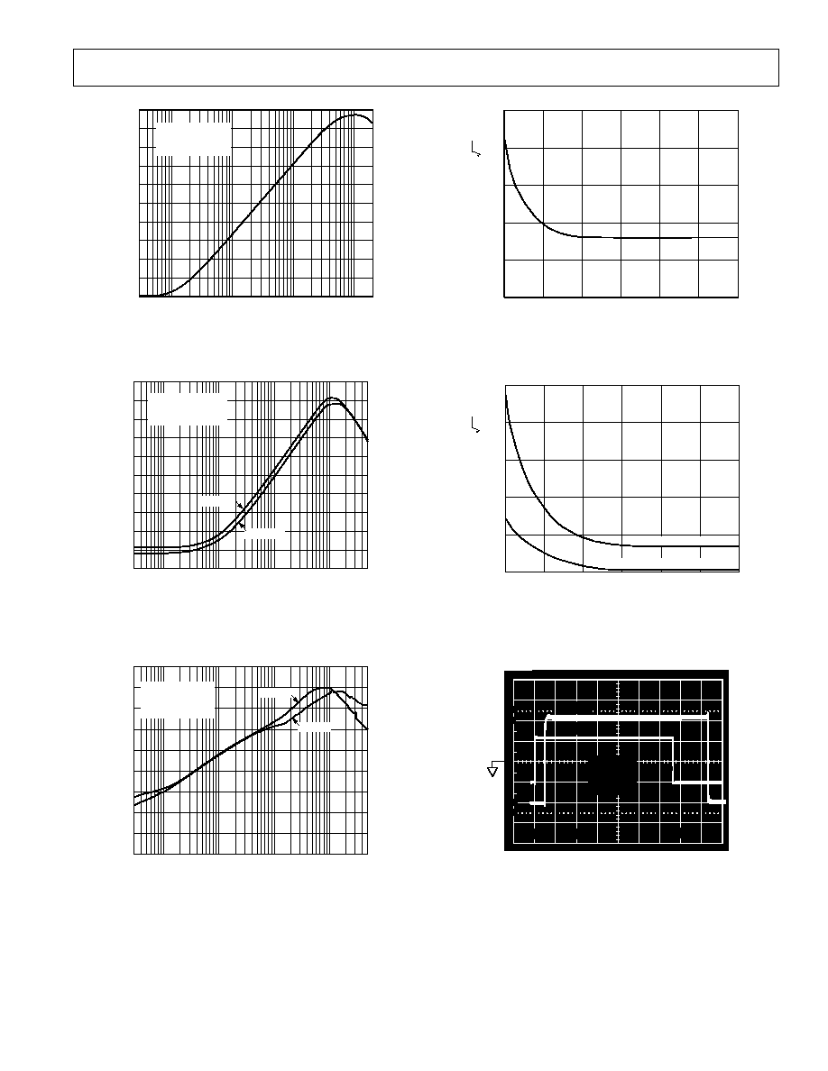
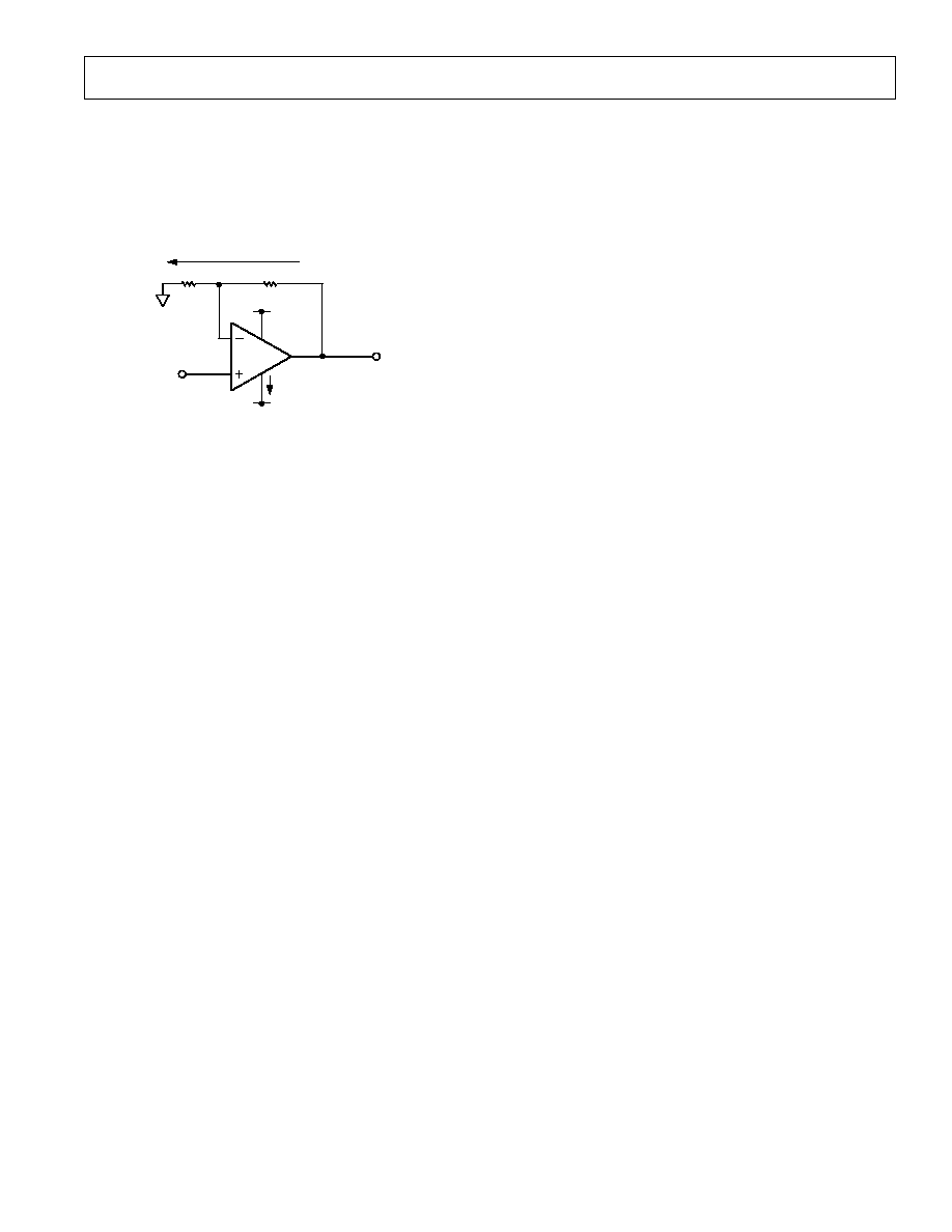
Driving Capacitive Loads
Capacitive loads interact with an op amp's output impedance
to create an extra delay in the feedback path. This reduces
circuit stability, and can cause unwanted ringing and oscilla-
tion. A given value of capacitance causes much less ringing
when the amplifier is used with a higher noise gain.
The capacitive load drive of the AD8005 can be increased by
adding a low valued resistor in series with the capacitive load.
Introducing a series resistor tends to isolate the capacitive load
from the feedback loop thereby diminishing its influence. Fig-
ure 29 shows the effects of a series resistor on capacitive drive
for varying voltage gains. As the closed-loop gain is increased,
the larger phase margin allows for larger capacitive loads with
less overshoot. Adding a series resistor at lower closed-loop
gains accomplishes the same effect. For large capacitive loads,
the frequency response of the amplifier will be dominated by
the roll-off of the series resistor and capacitive load.
AD8005
R
G
R
F
R
S
R
L
1k
C
L
Figure 28. Driving Capacitive Loads
CAPACITIVE LOAD pF
80
70
60
1
3
4
5
CLOSED-LOOP GAIN V/V
50
2
40
30
20
10
0
V
S
= 5V
R
S
= 10
R
S
= 5
R
S
= 0
2V OUTPUT STEP
WITH 30% OVERSHOOT
Figure 29. Capacitive Load Drive vs. Closed-Loop Gain
Single-Supply Level Shifter
In addition to providing buffering, many systems require that an
op amp provide level shifting. A common example is the level
shifting that is required to move a bipolar signal into the unipo-
lar range of many modern analog-to-digital converters (ADCs). In
general, single supply ADCs have input ranges that are refer-
enced neither to ground nor supply. Instead the reference level
is some point in between, usually halfway between ground and
supply (+2.5 V for a single supply 5 V ADC). Because high-
speed ADCs typically have input voltage ranges of 1 V to 2 V,
the op amp driving it must be single supply but not necessarily
rail-to-rail.
V
REF
+5V
R2
1.5k
V
OUT
0.01 F
10 F
+5V
R1
1.5k
V
IN
0.1 F
R4
10k
R3
30.1k
AD8005
Figure 30. Bipolar to Unipolar Level Shifter
Figure 30 shows a level shifter circuit that can move a bipolar
signal into a unipolar range. A positive reference voltage, derived
from the +5 V supply, sets a bias level of +1.25 V at the nonin-
verting terminal of the op amp. In ac applications, the accuracy of
this voltage level is not important. Noise is however a serious
consideration. A 0.1
µ
F capacitor provides useful decoupling of
this noise.
The bias level on the noninverting terminal sets the input common-
mode voltage to +1.25 V. Because the output will always be
positive, the op amp may therefore be powered with a single
+5 V power supply.
The overall gain function is given by the equation:
V
OUT
=
R2
R1
V
IN
+
R4
R3
+
R4
1
+
R2
R1
V
REF
In the above example, the equation simplifies to
V
OUT
=
V
IN
+
2.5V
AD8005
10
REV. A
Single-Ended-to-Differential Conversion
Many single supply ADCs have differential inputs. In such cases,
the ideal common-mode operating point is usually halfway
between supply and ground. Figure 31 shows how to convert a
single-ended bipolar signal into a differential signal with a
common-mode level of 2.5 V.
0.1 F
0.1 F
+5V
R
IN
1k
AD8005
2.49k
BIPOLAR
SIGNAL
0.5V
0.1 F
+5V
2.49k
2.49k
+5V
AD8005
0.1 F
2.49k
+5V
V
OUT
R
F1
2.49k
R
F2
3.09k
R
G
619
Figure 31. Single-Ended-to-Differential Converter
Amp 1 has its +input driven with the ac-coupled input signal
while the +input of Amp 2 is connected to a bias level of +2.5 V.
Thus the input of Amp 2 is driven to virtual +2.5 V by its
output. Therefore, Amp 1 is configured for a noninverting gain
of five, (1 + R
F1
/R
G
), because RG is connected to the virtual
+2.5 V of Amp 2's input.
When the +input of Amp 1 is driven with a signal, the same
signal appears at the input of Amp 1. This signal serves as an
input to Amp 2 configured for a gain of 5, (R
F2
/R
G
). Thus the
two outputs move in opposite directions with the same gain and
create a balanced differential signal.
This circuit can be simplified to create a bipolar in/bipolar out
single-ended to differential converter. Obviously, a single supply
is no longer adequate and the V
S
pins must now be powered
with 5 V. The +input to Amp 2 is tied to ground. The ac
coupling on the +input of Amp 1 is removed and the signal can
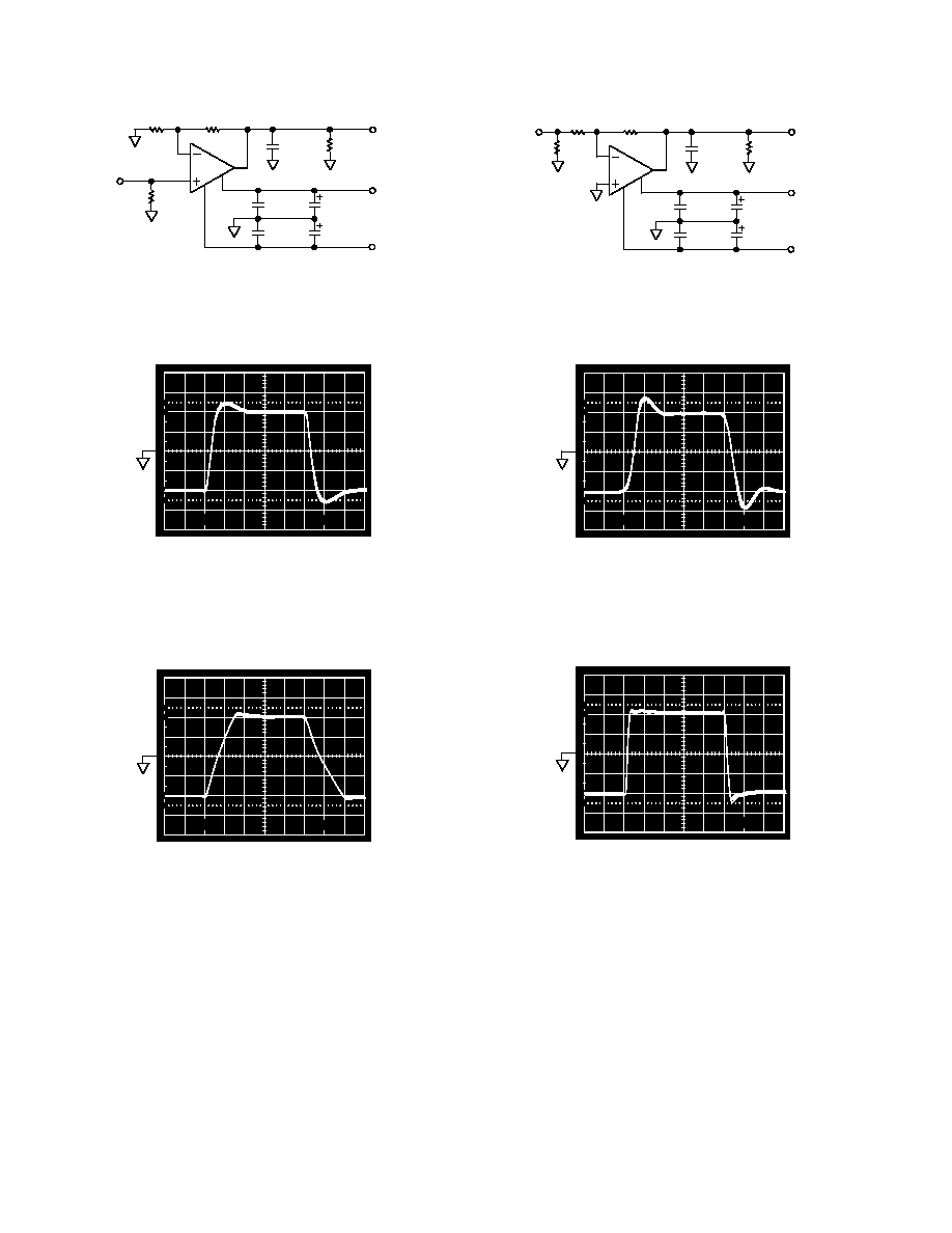
be fed directly into Amp 1.
Layout Considerations
In order to achieve the specified high-speed performance of the
AD8005 you must be attentive to board layout and component
selection. Proper R
F
design techniques and selection of compo-
nents with low parasitics are necessary.
The PCB should have a ground plane that covers all unused
portions of the component side of the board. This will provide a
low impedance path for signals flowing to ground. The ground
plane should be removed from the area under and around the
chip (leave about 2 mm between the pin contacts and the
ground plane). This helps to reduce stray capacitance. If both
signal tracks and the ground plane are on the same side of the
PCB, also leave a 2 mm gap between ground plane and track.
C1
0.01 F
C2
0.01 F
C4
10 F
C3
10 F
R
T
INVERTING CONFIGURATION
V
IN
V
OUT
+V
S
V
S
R
G
R
F
R
O
C1
0.01 F
C2
0.01 F
C4
10 F
C3
10 F
R
T
NONINVERTING CONFIGURATION
V
IN
V
OUT
+V
S
V
S
R
G
R
F
R
O
Figure 32. Inverting and Noninverting Configurations
Chip capacitors have low parasitic resistance and inductance
and are suitable for supply bypassing (see Figure 32). Make sure
that one end of the capacitor is within 1/8 inch of each power
pin with the other end connected to the ground plane. An
additional large (0.47
µ
F10
µ
F) tantalum electrolytic capacitor
should also be connected in parallel. This capacitor supplies
current for fast, large signal changes at the output. It must not
necessarily be as close to the power pin as the smaller capacitor.
Locate the feedback resistor close to the inverting input pin in
order to keep the stray capacitance at this node to a minimum.
Capacitance variations of less than 1.5 pF at the inverting input
will significantly affect high-speed performance.
Use stripline design techniques for long signal traces (i.e., greater
than about 1 inch). Striplines should have a characteristic
impedance of either 50
or 75
. For the Stripline to be
effective, correct termination at both ends of the line is necessary.
Table I. Typical Bandwidth vs. Gain Setting Resistors
Small Signal 3 dB
BW (MHz),
Gain
R
F
R
G
R
T
V
S
= 5 V
1
1.49 k
1.49 k
52.3
120 MHz
10
1 k
100
100
60 MHz
+1
2.49 k
49.9
270 MHz
+2
2.49 k
2.49 k
49.9
170 MHz
+10
499
56.2
49.9
40 MHz
AD8005
11
REV. A
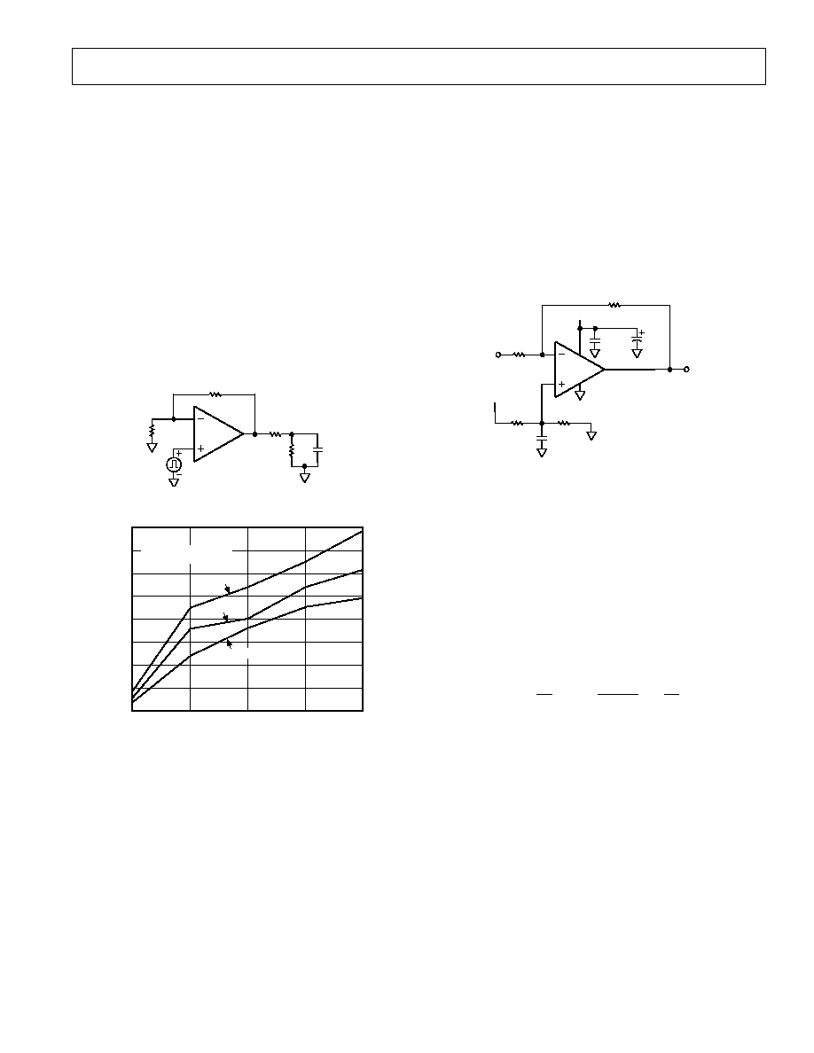
Increasing Feedback Resistors
Unlike conventional voltage feedback op amps, the choice of feed-
back resistor has a direct impact on the closed-loop bandwidth
and stability of a current feedback op amp circuit. Reducing the
resistance below the recommended value makes the amplifier
more unstable. Increasing the size of the feedback resistor
reduces the closed-loop bandwidth.
V
OUT
+5V
562
4.99k
2V (rms)
5V
AD8005
V
IN
0.2V (rms)
QUIESCENT CURRENT
475 A (MAX)
360 A (rms)
Figure 33. Saving Power by Increasing Feedback Resistor
Network
In power-critical applications where some bandwidth can be
sacrificed, increasing the size of the feedback resistor will yield
significant power savings. A good example of this is the gain of
+10 case. Operating from a bipolar supply (
±
5 V), the quiescent
current is 475
µ
A (excluding the feedback network). The recom-
mended feedback and gain resistors are 499
and 56.2
respectively. In order to drive an rms output voltage of 2 V, the
output must deliver a current of 3.6 mA to the feedback net-
work. Increasing the size of the resistor network by a factor of
10 as shown in Figure 33 will reduce this current to 360
µ
A.
The closed loop bandwidth will however decrease to 20 MHz.
AD8005
12
REV. A
C2186a08/99
PRINTED IN U.S.A.
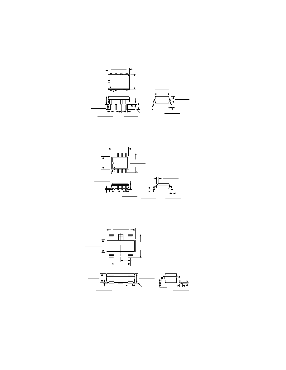
OUTLINE DIMENSIONS
Dimensions shown in inches and (mm).
8-Lead Plastic DIP
(N-8)
8
1
4
5
0.430 (10.92)
0.348 (8.84)
0.280 (7.11)
0.240 (6.10)
PIN 1
SEATING
PLANE
0.022 (0.558)
0.014 (0.356)
0.060 (1.52)
0.015 (0.38)
0.210 (5.33)
MAX
0.130
(3.30)
MIN
0.070 (1.77)
0.045 (1.15)
0.100
(2.54)
BSC
0.160 (4.06)
0.115 (2.93)
0.325 (8.25)
0.300 (7.62)
0.015 (0.381)
0.008 (0.204)
0.195 (4.95)
0.115 (2.93)
8-Lead Plastic SOIC
(SO-8)
0.1968 (5.00)
0.1890 (4.80)
8
5
4
1
0.2440 (6.20)
0.2284 (5.80)
PIN 1
0.1574 (4.00)
0.1497 (3.80)
0.0688 (1.75)
0.0532 (1.35)
SEATING
PLANE
0.0098 (0.25)
0.0040 (0.10)
0.0192 (0.49)
0.0138 (0.35)
0.0500
(1.27)
BSC
0.0098 (0.25)
0.0075 (0.19)
0.0500 (1.27)
0.0160 (0.41)
8
°
0
°
0.0196 (0.50)
0.0099 (0.25)
x 45
°
5-Lead Plastic SOT-23
(RT-5)
0.0079 (0.20)
0.0031 (0.08)
0.0217 (0.55)
0.0138 (0.35)
10
°
0
°
0.0197 (0.50)
0.0138 (0.35)
0.0059 (0.15)
0.0019 (0.05)
0.0512 (1.30)
0.0354 (0.90)
SEATING
PLANE
0.0571 (1.45)
0.0374 (0.95)
0.1181 (3.00)
0.1102 (2.80)
0.0669 (1.70)
0.0590 (1.50)
0.1181 (3.00)
0.1024 (2.60)
4
5
1
2
3
0.0748 (1.90)
BSC
0.0374 (0.95) BSC