 | –≠–ª–µ–∫—Ç—Ä–æ–Ω–Ω—ã–π –∫–æ–º–ø–æ–Ω–µ–Ω—Ç: AD8009 | –°–∫–∞—á–∞—Ç—å:  PDF PDF  ZIP ZIP |

REV. B
Information furnished by Analog Devices is believed to be accurate and
reliable. However, no responsibility is assumed by Analog Devices for its
use, nor for any infringements of patents or other rights of third parties
which may result from its use. No license is granted by implication or
otherwise under any patent or patent rights of Analog Devices.
a
AD8009
One Technology Way, P.O. Box 9106, Norwood, MA 02062-9106, U.S.A.
Tel: 781/329-4700
World Wide Web Site: http://www.analog.com
Fax: 781/326-8703
© Analog Devices, Inc., 2000
1 GHz, 5,500 V/ s
Low Distortion Amplifier
FUNCTIONAL BLOCK DIAGRAM
8-Lead Plastic SOIC (SO-8) 5-Lead SOT-23 (RT-5)
PRODUCT DESCRIPTION
The AD8009 is an ultrahigh speed current feedback amplifier
with a phenomenal 5,500 V/
µs slew rate that results in a rise
time of 545 ps, making it ideal as a pulse amplifier.
The high slew rate reduces the effect of slew rate limiting and
results in the large signal bandwidth of 440 MHz required for
high resolution video graphic systems. Signal quality is main-
tained over a wide bandwidth with worst case distortion of
≠40 dBc @ 250 MHz (G = +10, 1 V p-p). For applications
with multitone signals such as IF signal chains, the third order
Intercept (3IP) of 12 dBm is achieved at the same frequency.
This distortion performance coupled with the current feedback
architecture make the AD8009 a flexible component for a gain
stage amplifier in IF/RF signal chains.
The AD8009 is capable of delivering over 175 mA of load
current and will drive four back terminated video loads while
maintaining low differential gain and phase error of 0.02% and
0.04
∞ respectively. The high drive capability is also reflected in
the ability to deliver 10 dBm of output power @ 70 MHz with
≠38 dBc SFDR.
The AD8009 is available in a small SOIC package and will
operate over the industrial temperature range ≠40
∞C to +85∞C.
DISTORTION ≠ dBc
≠30
≠80
≠40
≠50
≠60
≠70
≠100
≠90
2ND,
150 LOAD
2ND,
100 LOAD
3RD,
150 LOAD
3RD,
100 LOAD
G = 2
R
F
= 301
V
O
= 2V p-p
FREQUENCY RESPONSE ≠ MHz
1
200
10
100
Figure 2. Distortion vs. Frequency; G = +2
FEATURES
Ultrahigh Speed
5,500 V/ s Slew Rate, 4 V Step, G = +2
545 ps Rise Time, 2 V Step, G = +2
Large Signal Bandwidth
440 MHz, G = +2
320 MHz, G = +10
Small Signal Bandwidth (≠3 dB)
1 GHz, G = +1
700 MHz, G = +2
Settling Time 10 ns to 0.1%, 2 V Step, G = +2
Low Distortion Over Wide Bandwidth
SFDR
≠44 dBc @ 150 MHz, G = +2, V
O
= 2 V p-p
≠41 dBc @ 150 MHz, G = +10, V
O
= 2 V p-p
3rd Order Intercept (3IP)
26 dBm @ 70 MHz, G = +10
18 dBm @ 150 MHz, G = +10
Good Video Specifications
Gain Flatness 0.1 dB to 75 MHz
0.01% Differential Gain Error, R
L
= 150
0.01 Differential Phase Error, R
L
= 150
High Output Drive
175 mA Output Load Drive
10 dBm with ≠38 dBc SFDR @ 70 MHz, G = +10
Supply Operation
5 V Voltage Supply
14 mA (Typ) Supply Current
APPLICATIONS
Pulse Amplifier
IF/RF Gain Stage/Amplifiers
High Resolution Video Graphics
High Speed Instrumentations
CCD Imaging Amplifier
FREQUENCY RESPONSE ≠ MHz
1
2
1
≠8
0
≠1
≠2
≠3
≠4
≠5
≠6
≠7
1000
10
NORMALIZED GAIN
≠
dB
100
G = +2
R
F
= 301
R
L
= 150
G = +10
R
F
= 200
R
L
= 100
V
O
= 2Vp≠p
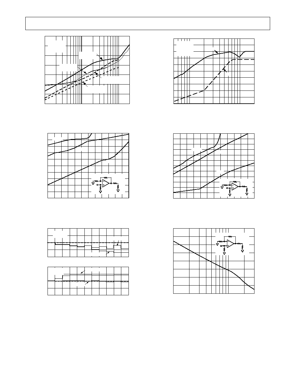
Figure 1. Large Signal Frequency Response; G = +2 & +10
1
V
OUT
AD8009
≠V
S
+IN
2
3
4
5
+V
S
≠IN
1
2
3
4
8
7
6
5
NC = NO CONNECT
AD8009
NC
≠IN
+IN
≠V
S
NC
OUT
+V
S
NC

≠2≠
REV. B
AD8009≠SPECIFICATIONS
(@ T
A
= +25 C, V
S
= 5 V, R
L
= 100
, for R Package: R
F
= 301
for G = +1, +2,
R
F
= 200
for G = +10, for RT Package: R
F
= 332
for G = +1, R
F
= 226
for G = +2 and R
F
= 191 for G = +10, unless otherwise noted.)
AD8009AR
Model
Conditions
Min
Typ
Max
Units
DYNAMIC PERFORMANCE
≠3 dB Small Signal Bandwidth, V
O
= 0.2 V p-p
R Package
G = +1, R
F
= 301
1000
MHz
RT Package
G = +1, R
F
= 332
845
MHz
G = +2
480
700
MHz
G = +10
300
350
MHz
Large Signal Bandwidth, V
O
= 2 V p-p
G = +2
390
440
MHz
G = +10
235
320
MHz
Gain Flatness 0.1 dB, V
O
= 0.2 V p-p
G = +2, R
L
= 150
45
75
MHz
Slew Rate
G = +2, R
L
= 150
, 4 V Step
4500
5500
V/
µs
Settling Time to 0.1%
G = +2, R
L
= 150
, 2 V Step
10
ns
G = +10, 2 V Step
25
ns
Rise and Fall Time
G = +2, R
L
= 150
, 4 V Step
0.725
ns
HARMONIC/NOISE PERFORMANCE
SFDR G = +2, V
O
= 2 V p-p
5 MHz
≠74
dBc
70 MHz
≠53
dBc
150 MHz
≠44
dBc
SFDR
G = +10, V
O
= 2 V p-p
5 MHz
≠58
dBc
70 MHz
≠41
dBc
150 MHz
≠41
dBc
Third Order Intercept (3IP)
70 MHz
26
dBm
W.R.T. Output, G = +10
150 MHz
18
dBm
250 MHz
12
dBm
Input Voltage Noise
f = 10 MHz
1.9
nV/
Hz
Input Current Noise
f = 10 MHz, +In
46
pA/
Hz
f = 10 MHz,
≠In
41
pA/
Hz
Differential Gain Error
NTSC, G = +2, R
L
= 150
0.01
0.03
%
NTSC, G = +2,
R
L
= 37.5
0.02
0.05
%
Differential Phase Error
NTSC, G = +2, R
L
= 150
0.01
0.03
Degrees
NTSC, G = +2,
R
L
= 37.5
0.04
0.08
Degrees
DC PERFORMANCE
Input Offset Voltage
2
5
mV
T
MIN
≠T
MAX
7
mV
Offset Voltage Drift
4
µV/∞C
≠Input Bias Current
50
150
±µA
T
MIN
≠T
MAX
75
±µA
+Input Bias Voltage
50
150
±µA
T
MIN
≠T
MAX
75
±µA
Open Loop Transresistance
90
250
k
T
MIN
≠T
MAX
170
k
INPUT CHARACTERISTICS
Input Resistance
+Input
110
k
≠Input
8
Input Capacitance
+Input
2.6
pF
Input Common-Mode Voltage Range
3.8
±V
Common-Mode Rejection Ratio
V
CM
=
±2.5
50
52
dB
OUTPUT CHARACTERISTICS
Output Voltage Swing
±3.7
±3.8
V
Output Current
R
L
= 10
, P
D
Package = 0.7 W
150
175
mA
Short Circuit Current
330
mA
POWER SUPPLY
Operating Range
±4
±6
V
Quiescent Current
14
16
mA
T
MIN
≠T
MAX
18
mA
Power Supply Rejection Ratio
V
S
=
±4 V to ±6 V
64
70
dB
Specifications subject to change without notice.

AD8009
≠3≠
REV. B
CAUTION
ESD (electrostatic discharge) sensitive device. Electrostatic charges as high as 4000 V readily
accumulate on the human body and test equipment and can discharge without detection.
Although the AD8009 features proprietary ESD protection circuitry, permanent damage may
occur on devices subjected to high energy electrostatic discharges. Therefore, proper ESD
precautions are recommended to avoid performance degradation or loss of functionality.
ABSOLUTE MAXIMUM RATINGS
1
Supply Voltage . . . . . . . . . . . . . . . . . . . . . . . . . . . . . . . . 12.6 V
Internal Power Dissipation
2
Small Outline Package (R) . . . . . . . . . . . . . . . . . 0.75 Watts
Input Voltage (Common Mode) . . . . . . . . . . . . . . . . . . . .
±V
S
Differential Input Voltage . . . . . . . . . . . . . . . . . . . . . .
±3.5 V
Output Short Circuit Duration
. . . . . . . . . . . . . . . . . . . . . . Observe Power Derating Curves
Storage Temperature Range R Package . . . . ≠65
∞C to +125∞C
Operating Temperature Range (A Grade) . . . ≠40
∞C to +85∞C
Lead Temperature Range (Soldering 10 sec) . . . . . . . . +300
∞C
NOTES
1
Stresses above those listed under Absolute Maximum Ratings may cause perma-
nent damage to the device. This is a stress rating only; functional operation of the
device at these or any other conditions above those indicated in the operational
section of this specification is not implied. Exposure to absolute maximum rating
conditions for extended periods may affect device reliability.
2
Specification is for device in free air:
8-Lead SOIC Package:
JA
= 155
∞C/W.
MAXIMUM POWER DISSIPATION
The maximum power that can be safely dissipated by the
AD8009 is limited by the associated rise in junction tempera-
ture. The maximum safe junction temperature for plastic
encapsulated devices is determined by the glass transition
temperature of the plastic, approximately +150
∞C. Exceeding
this limit temporarily may cause a shift in parametric perfor-
mance due to a change in the stresses exerted on the die by the
package. Exceeding a junction temperature of +175
∞C for an
extended period can result in device failure.
While the AD8009 is internally short circuit protected, this
may not be sufficient to guarantee that the maximum junction
temperature (+150
∞C) is not exceeded under all conditions.
To ensure proper operation, it is necessary to observe the
maximum power derating curves.
AMBIENT TEMPERATURE ≠ ∞C
90
80
2.0
1.0
0
1.5
0.5
≠50
T
J
= +150∞C
MAXIMUM POWER DISSIPATION
≠
Watts
70
60
50
40
30
20
10
0
≠40 ≠30 ≠20 ≠10
8-LEAD SOIC PACKAGE
5-LEAD SOT-23 PACKAGE
Figure 3. Plot of Maximum Power Dissipation vs.
Temperature
ORDERING GUIDE
Temperature
Package
Package
Branding
Model
Range
Description
Option
Information
AD8009AR
≠40
∞C to +85∞C
8-Lead SOIC
SO-8
AD8009AR-REEL
≠40
∞C to +85∞C
13" Tape and Reel
SO-8
AD8009ART
≠40
∞C to +85∞C
5-Lead SOT-23
RT-5
HKJ
AD8009ART-REEL
≠40
∞C to +85∞C
13" Tape and Reel
RT-5
HKJ
AD8009ART-REEL7
≠40
∞C to +85∞C
7" Tape and Reel
RT-5
HKJ
AD8009-EB
Evaluation Board
SO-8
WARNING!
ESD SENSITIVE DEVICE

AD8009
≠4≠
REV. B
≠Typical Performance Characteristics
FREQUENCY ≠ MHz
NORMALIZED GAIN
≠
dB
10
100
3
2
1
0
≠1
≠6
≠7
≠2
≠3
≠4
≠5
1
1000
R PACKAGE:
R
L
= 100
V
O
= 200mV p≠p
G = +1, +2: R
F
= 301
G = +10: R
F
= 200
RT PACKAGE:
G = +1: R
F
= 332
G = +2: R
F
= 226
G = +10: R
F
= 191
G = +1, R
G = +10, R & RT
G = +2, R & RT
G = +1, RT
Figure 4. Frequency Response; G = +1, +2, +10, R and RT
Packages
GAIN
≠
dB
7
6
5
4
3
2
1
0
≠1
≠2
8
100
1
1000
10
FREQUENCY ≠ MHz
G = +2
R
F
= 301
R
L
= 150
V
O
AS SHOWN
4V p≠p
2V p≠p
Figure 5. Large Signal Frequency Response; G = +2
GAIN
≠
dB
7
6
5
4
3
2
1
0
≠1
≠2
8
100
1
1000
10
FREQUENCY ≠ MHz
G = +2
R
F
= 301
R
L
= 150
V
O
= 2V p≠p
≠40 C
+85 C
≠40 C
+85 C
Figure 6. Large Signal Frequency Response vs.
Temperature; G = +2
6.1
6.0
5.9
5.8
5.7
5.6
5.5
5.4
5.3
5.2
6.2
GAIN FLATNESS
≠
dB
FREQUENCY ≠ MHz
10
100
1
1000
G = +2
R
F
= 301
R
L
= 150
V
O
= 200mV p≠p
Figure 7. Gain Flatness; G = +2
GAIN
≠
dB
21
20
19
18
17
16
15
14
13
12
22
100
1
1000
10
FREQUENCY ≠ MHz
G = +10
R
F
= 200
R
L
= 100
V
O
AS SHOWN
2V p≠p
4V p≠p
Figure 8. Large Signal Frequency Response; G = +10
GAIN
≠
dB
21
20
19
18
17
16
15
14
13
12
22
100
1
1000
10
FREQUENCY ≠ MHz
G = +10
R
F
= 200
R
L
= 100
V
O
= 2V p≠p
≠40 C
+85 C
Figure 9. Large Signal Frequency Response vs.
Temperature; G = +10
AD8009
≠5≠
REV. B
DISTORTION
≠
dBc
≠30
≠80
≠40
≠50
≠60
≠70
≠100
≠90
2ND,
150 LOAD
2ND,
100 LOAD
3RD,
150 LOAD
3RD,
100 LOAD
G = 2
R
F
= 301
V
O
= 2V p-p
FREQUENCY RESPONSE ≠ MHz
1
200
10
100
Figure 10. Distortion vs. Frequency; G = +2
≠35
≠70
≠85
≠40
≠65
≠75
≠80
≠45
≠55
≠50
≠60
DISTORTION
≠
dBc
P
OUT
≠ dBm
≠10
12
≠6
≠4
≠2
0
2
4
6
8
10
14
≠8
200
P
OUT
22.1
50
50
50
250MHz
70MHz
5MHz
Figure 11. 2nd Harmonic Distortion vs. P
OUT
; (G = +10)
IRE
100
0
0.02
DIFF GAIN
≠
%
≠0.02
0.00
≠0.01
0.01
R
L
= 37.5
R
L
= 150
G = +2
R
F
= 301
G = +2
R
F
= 301
R
L
= 37.5
R
L
= 150
0.10
DIFF PHASE
≠
Degrees
≠0.10
≠0.00
≠0.05
0.05
IRE
100
0
Figure 12. Differential Gain and Phase
≠30
≠35
≠80
≠40
≠45
≠50
≠55
≠60
≠65
≠70
≠75
DISTORTION
≠
dBc
100
10
5
200
FREQUENCY ≠ MHz
G = +10
R
F
= 200
R
L
= 100
V
O
= 2V p≠p
2ND
3RD
Figure 13. Distortion vs. Frequency; G = +10
P
OUT
≠ dBm
DISTORTION
≠
dBc
≠45
≠80
≠95
≠10
≠8
12
≠6
≠4
≠2
0
2
4
6
8
10
≠50
≠75
≠85
≠90
≠55
≠65
≠60
≠70
≠40
≠35
14
5MHz
70MHz
250MHz
200
P
OUT
22.1
50
50
50
Figure 14. 3rd Harmonic Distortion vs. P
OUT
; (G = +10)
INTERCEPT POINT
≠
dBm
FREQUENCY ≠ MHz
10
250
100
10
50
45
40
35
30
25
20
15
200
P
OUT
22.1
50
50
50
Figure 15. Two Tone, 3rd Order IMD Intercept vs.
Frequency; G = +10