/home/web/htmldatasheet/RUSSIAN/html/ad/164338
REV. D
Information furnished by Analog Devices is believed to be accurate and
reliable. However, no responsibility is assumed by Analog Devices for its
use, nor for any infringements of patents or other rights of third parties
which may result from its use. No license is granted by implication or
otherwise under any patent or patent rights of Analog Devices.
a
AD8009
One Technology Way, P.O. Box 9106, Norwood, MA 02062-9106, U.S.A.
Tel: 781/329-4700
World Wide Web Site: http://www.analog.com
Fax: 781/326-8703
© Analog Devices, Inc., 2000
1 GHz, 5,500 V/ s
Low Distortion Amplifier
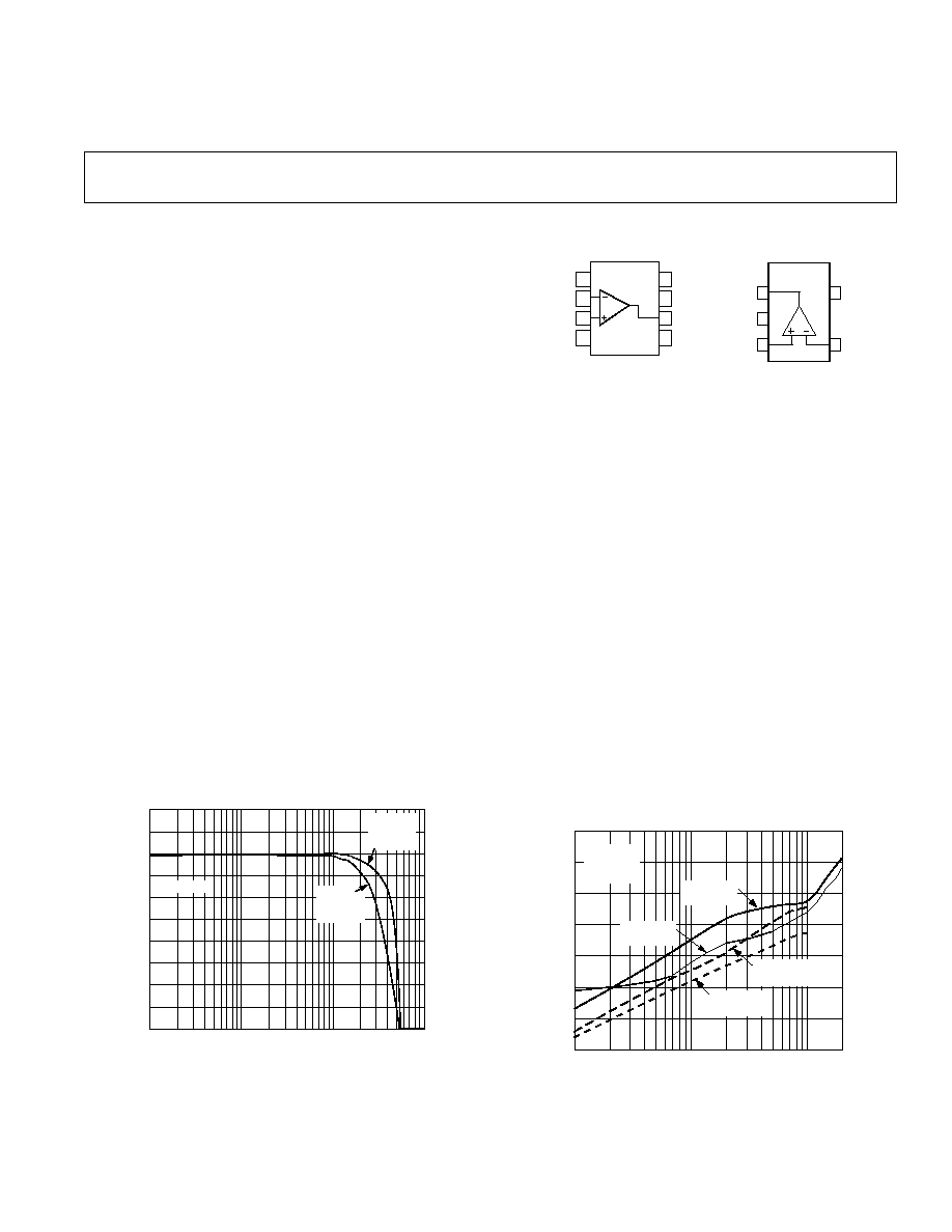
FUNCTIONAL BLOCK DIAGRAMS
8-Lead Plastic SOIC (SO-8) 5-Lead SOT-23 (RT-5)
PRODUCT DESCRIPTION
The AD8009 is an ultrahigh speed current feedback amplifier
with a phenomenal 5,500 V/
µs slew rate that results in a rise
time of 545 ps, making it ideal as a pulse amplifier.
The high slew rate reduces the effect of slew rate limiting and
results in the large signal bandwidth of 440 MHz required for
high resolution video graphic systems. Signal quality is main-
tained over a wide bandwidth with worst case distortion of
40 dBc @ 250 MHz (G = +10, 1 V p-p). For applications
with multitone signals such as IF signal chains, the third order
Intercept (3IP) of 12 dBm is achieved at the same frequency.
This distortion performance coupled with the current feedback
architecture make the AD8009 a flexible component for a gain
stage amplifier in IF/RF signal chains.
The AD8009 is capable of delivering over 175 mA of load
current and will drive four back terminated video loads while
maintaining low differential gain and phase error of 0.02% and
0.04
° respectively. The high drive capability is also reflected in
the ability to deliver 10 dBm of output power @ 70 MHz with
38 dBc SFDR.
The AD8009 is available in a small SOIC package and will
operate over the industrial temperature range 40
°C to +85°C.
The AD8009 is also available in an SOT-23-5 and will operate
over the commercial temperature range 0
°C to 70°C.
DISTORTION dBc
30
80
40
50
60
70
100
90
2ND,
150 LOAD
2ND,
100 LOAD
3RD,
150 LOAD
3RD,
100 LOAD
G = 2
R
F
= 301
V
O
= 2V p-p
FREQUENCY RESPONSE MHz
1
200
10
100
Figure 2. Distortion vs. Frequency; G = +2
FEATURES
Ultrahigh Speed
5,500 V/ s Slew Rate, 4 V Step, G = +2
545 ps Rise Time, 2 V Step, G = +2
Large Signal Bandwidth
440 MHz, G = +2
320 MHz, G = +10
Small Signal Bandwidth (3 dB)
1 GHz, G = +1
700 MHz, G = +2
Settling Time 10 ns to 0.1%, 2 V Step, G = +2
Low Distortion Over Wide Bandwidth
SFDR
44 dBc @ 150 MHz, G = +2, V
O
= 2 V p-p
41 dBc @ 150 MHz, G = +10, V
O
= 2 V p-p
3rd Order Intercept (3IP)
26 dBm @ 70 MHz, G = +10
18 dBm @ 150 MHz, G = +10
Good Video Specifications
Gain Flatness 0.1 dB to 75 MHz
0.01% Differential Gain Error, R
L
= 150
0.01 Differential Phase Error, R
L
= 150
High Output Drive
175 mA Output Load Drive
10 dBm with 38 dBc SFDR @ 70 MHz, G = +10
Supply Operation
+5 V to 5 V Voltage Supply
14 mA (Typ) Supply Current
APPLICATIONS
Pulse Amplifier
IF/RF Gain Stage/Amplifiers
High Resolution Video Graphics
High Speed Instrumentations
CCD Imaging Amplifier
FREQUENCY RESPONSE MHz
1
2
1
8
0
1
2
3
4
5
6
7
1000
10
NORMALIZED GAIN
dB
100
G = +2
R
F
= 301
R
L
= 150
G = +10
R
F
= 200
R
L
= 100
V
O
= 2Vpp
Figure 1. Large Signal Frequency Response; G = +2 and +10
1
V
OUT
AD8009
V
S
+IN
2
3
4
5
+V
S
IN
1
2
3
4
8
7
6
5
NC = NO CONNECT
AD8009
NC
IN
+IN
V
S
NC
OUT
+V
S
NC

2
REV. D
AD8009SPECIFICATIONS
(@ T
A
= 25 C, V
S
= 5 V, R
L
= 100 , for R Package: R
F
= 301 for G = +1, +2, R
F
= 200
for G = +10, for RT Package: R
F
= 332
for G = +1, R
F
= 226
for G = +2 and R
F
= 191 for G = +10, unless otherwise noted.)
AD8009AR/JRT
Model
Conditions
Min
Typ
Max
Unit
DYNAMIC PERFORMANCE
3 dB Small Signal Bandwidth, V
O
= 0.2 V p-p
R Package
G = +1, R
F
= 301
1000
MHz
RT Package
G = +1, R
F
= 332
845
MHz
G = +2
480
700
MHz
G = +10
300
350
MHz
Large Signal Bandwidth, V
O
= 2 V p-p
G = +2
390
440
MHz
G = +10
235
320
MHz
Gain Flatness 0.1 dB, V
O
= 0.2 V p-p
G = +2, R
L
= 150
45
75
MHz
Slew Rate
G = +2, R
L
= 150
, 4 V Step
4500
5500
V/
µs
Settling Time to 0.1%
G = +2, R
L
= 150
, 2 V Step
10
ns
G = +10, 2 V Step
25
ns
Rise and Fall Time
G = +2, R
L
= 150
, 4 V Step
0.725
ns
HARMONIC/NOISE PERFORMANCE
SFDR G = +2, V
O
= 2 V p-p
5 MHz
74
dBc
70 MHz
53
dBc
150 MHz
44
dBc
SFDR
G = +10, V
O
= 2 V p-p
5 MHz
58
dBc
70 MHz
41
dBc
150 MHz
41
dBc
Third Order Intercept (3IP)
70 MHz
26
dBm
W.R.T. Output, G = +10
150 MHz
18
dBm
250 MHz
12
dBm
Input Voltage Noise
f = 10 MHz
1.9
nV/
Hz
Input Current Noise
f = 10 MHz, +In
46
pA/
Hz
f = 10 MHz,
In
41
pA/
Hz
Differential Gain Error
NTSC, G = +2, R
L
= 150
0.01
0.03
%
NTSC, G = +2,
R
L
= 37.5
0.02
0.05
%
Differential Phase Error
NTSC, G = +2, R
L
= 150
0.01
0.03
Degrees
NTSC, G = +2,
R
L
= 37.5
0.04
0.08
Degrees
DC PERFORMANCE
Input Offset Voltage
2
5
mV
T
MIN
T
MAX
7
mV
Offset Voltage Drift
4
µV/°C
Input Bias Current
50
150
±µA
T
MIN
T
MAX
75
±µA
+Input Bias Voltage
50
150
±µA
T
MIN
T
MAX
75
±µA
Open Loop Transresistance
90
250
k
T
MIN
T
MAX
170
k
INPUT CHARACTERISTICS
Input Resistance
+Input
110
k
Input
8
Input Capacitance
+Input
2.6
pF
Input Common-Mode Voltage Range
3.8
±V
Common-Mode Rejection Ratio
V
CM
=
±2.5
50
52
dB
OUTPUT CHARACTERISTICS
Output Voltage Swing
±3.7
±3.8
V
Output Current
R
L
= 10
, P
D
Package = 0.7 W
150
175
mA
Short Circuit Current
330
mA
POWER SUPPLY
Operating Range
+5
±6
V
Quiescent Current
14
16
mA
T
MIN
T
MAX
18
mA
Power Supply Rejection Ratio
V
S
=
±4 V to ±6 V
64
70
dB
Specifications subject to change without notice.
AD8009
3
REV. D
CAUTION
ESD (electrostatic discharge) sensitive device. Electrostatic charges as high as 4000 V readily
accumulate on the human body and test equipment and can discharge without detection.
Although the AD8009 features proprietary ESD protection circuitry, permanent damage may
occur on devices subjected to high-energy electrostatic discharges. Therefore, proper ESD
precautions are recommended to avoid performance degradation or loss of functionality.
ABSOLUTE MAXIMUM RATINGS
1
Supply Voltage . . . . . . . . . . . . . . . . . . . . . . . . . . . . . . . . 12.6 V
Internal Power Dissipation
2
Small Outline Package (R) . . . . . . . . . . . . . . . . . . . . 0.75 Watts
Input Voltage (Common Mode) . . . . . . . . . . . . . . . . . . . .
±V
S
Differential Input Voltage . . . . . . . . . . . . . . . . . . . . . . .
±3.5 V
Output Short Circuit Duration
. . . . . . . . . . . . . . . . . . . . . . Observe Power Derating Curves
Storage Temperature Range R Package . . . . 65
°C to +125°C
Operating Temperature Range (A Grade) . . . 40
°C to +85°C
Operating Temperature Range (J Grade) . . . . . . . 0
°C to 70°C
Lead Temperature Range (Soldering 10 sec) . . . . . . . . . 300
°C
NOTES
1
Stresses above those listed under Absolute Maximum Ratings may cause perma-
nent damage to the device. This is a stress rating only; functional operation of the
device at these or any other conditions above those indicated in the operational
section of this specification is not implied. Exposure to absolute maximum rating
conditions for extended periods may affect device reliability.
2
Specification is for device in free air:
8-Lead SOIC Package:
JA
= 155
°C/W.
5-Lead SOT-23 Package:
JA
= 240
°C/W.
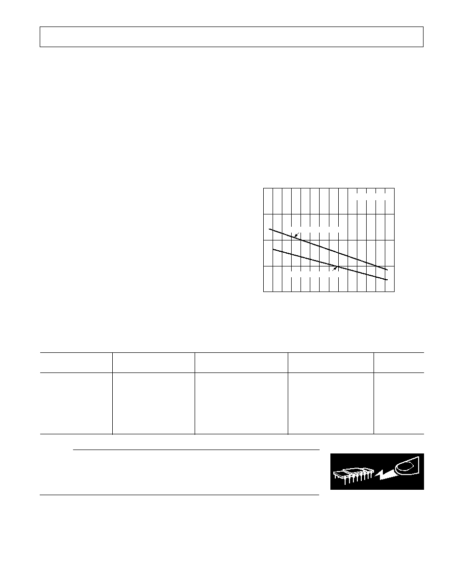
MAXIMUM POWER DISSIPATION
The maximum power that can be safely dissipated by the
AD8009 is limited by the associated rise in junction tempera-
ture. The maximum safe junction temperature for plastic
encapsulated devices is determined by the glass transition
temperature of the plastic, approximately 150
°C. Exceeding
this limit temporarily may cause a shift in parametric perfor-
mance due to a change in the stresses exerted on the die by the
package. Exceeding a junction temperature of 175
°C for an
extended period can result in device failure.
While the AD8009 is internally short circuit protected, this
may not be sufficient to guarantee that the maximum junction
temperature (150
°C) is not exceeded under all conditions. To
ensure proper operation, it is necessary to observe the maxi-
mum power derating curves.
AMBIENT TEMPERATURE °C
90
80
2.0
1.0
0
1.5
0.5
50
T
J
= +150°C
MAXIMUM POWER DISSIPATION
Watts
70
60
50
40
30
20
10
0
40 30 20 10
8-LEAD SOIC PACKAGE
5-LEAD SOT-23 PACKAGE
Figure 3. Plot of Maximum Power Dissipation vs.
Temperature
ORDERING GUIDE
Temperature
Package
Package
Branding
Model
Range
Description
Option
Information
AD8009ACHIPS
40
°C to +85°C
Die
AD8009AR
40
°C to +85°C
8-Lead SOIC
SO-8
AD8009AR-REEL
40
°C to +85°C
8-Lead SOIC
13" Tape and Reel
AD8009AR-REEL7
40
°C to +85°C
8-Lead SOIC
7" Tape and Reel
AD8009JRT-REEL
0
°C to 70°C
5-Lead SOT-23
13" Tape and Reel
HKJ
AD8009JRT-REEL7
0
°C to 70°C
5-Lead SOT-23
7" Tape and Reel
HKJ
AD8009-EB
Evaluation Board
SO-8
WARNING!
ESD SENSITIVE DEVICE
AD8009
4
REV. D
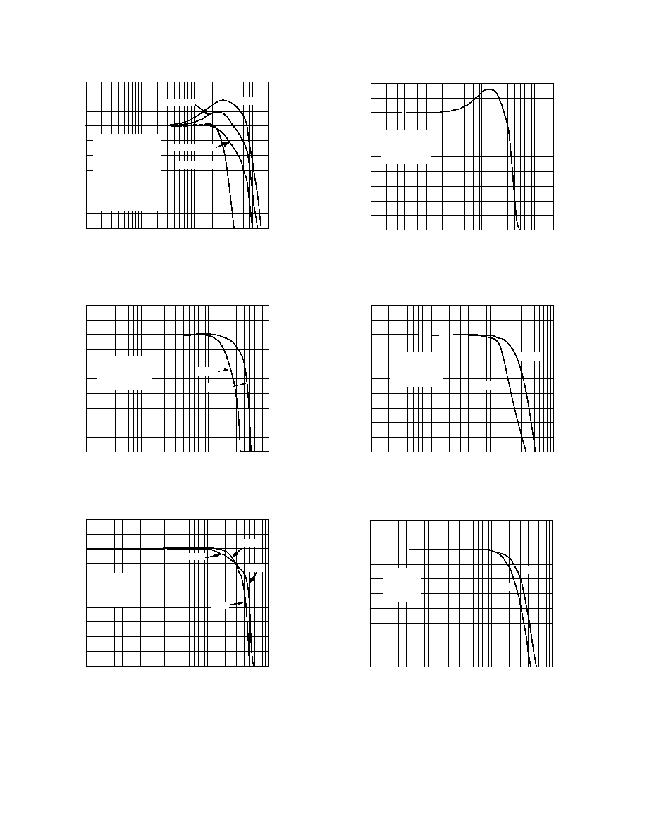
Typical Performance Characteristics
FREQUENCY MHz
NORMALIZED GAIN
dB
10
100
3
2
1
0
1
6
7
2
3
4
5
1
1000
R PACKAGE:
R
L
= 100
V
O
= 200mV pp
G = +1, +2: R
F
= 301
G = +10: R
F
= 200
RT PACKAGE:
G = +1: R
F
= 332
G = +2: R
F
= 226
G = +10: R
F
= 191
G = +1, R
G = +10, R & RT
G = +2, R & RT
G = +1, RT
Figure 4. Frequency Response; G = +1, +2, +10, R and RT
Packages
GAIN
dB
7
6
5
4
3
2
1
0
1
2
8
100
1
1000
10
FREQUENCY MHz
G = +2
R
F
= 301
R
L
= 150
V
O
AS SHOWN
4V pp
2V pp
Figure 5. Large Signal Frequency Response; G = +2
GAIN
dB
7
6
5
4
3
2
1
0
1
2
8
100
1
1000
10
FREQUENCY MHz
G = +2
R
F
= 301
R
L
= 150
V
O
= 2V pp
40 C
+85 C
40 C
+85 C
Figure 6. Large Signal Frequency Response vs.
Temperature; G = +2
6.1
6.0
5.9
5.8
5.7
5.6
5.5
5.4
5.3
5.2
6.2
GAIN FLATNESS
dB
FREQUENCY MHz
10
100
1
1000
G = +2
R
F
= 301
R
L
= 150
V
O
= 200mV pp
Figure 7. Gain Flatness; G = +2
GAIN
dB
21
20
19
18
17
16
15
14
13
12
22
100
1
1000
10
FREQUENCY MHz
G = +10
R
F
= 200
R
L
= 100
V
O
AS SHOWN
2V pp
4V pp
Figure 8. Large Signal Frequency Response; G = +10
GAIN
dB
21
20
19
18
17
16
15
14
13
12
22
100
1
1000
10
FREQUENCY MHz
G = +10
R
F
= 200
R
L
= 100
V
O
= 2V pp
40 C
+85 C
Figure 9. Large Signal Frequency Response vs.
Temperature; G = +10
AD8009
5
REV. D
DISTORTION
dBc
30
80
40
50
60
70
100
90
2ND,
150 LOAD
2ND,
100 LOAD
3RD,
150 LOAD
3RD,
100 LOAD
G = 2
R
F
= 301
V
O
= 2V p-p
FREQUENCY RESPONSE MHz
1
200
10
100
Figure 10. Distortion vs. Frequency; G = +2
35
70
85
40
65
75
80
45
55
50
60
DISTORTION
dBc
P
OUT
dBm
10
12
6
4
2
0
2
4
6
8
10
14
8
200
P
OUT
22.1
50
50
50
250MHz
70MHz
5MHz
Figure 11. 2nd Harmonic Distortion vs. P
OUT
; (G = +10)
IRE
100
0
0.02
DIFF GAIN
%
0.02
0.00
0.01
0.01
R
L
= 37.5
R
L
= 150
G = +2
R
F
= 301
G = +2
R
F
= 301
R
L
= 37.5
R
L
= 150
0.10
DIFF PHASE
Degrees
0.10
0.00
0.05
0.05
IRE
100
0
Figure 12. Differential Gain and Phase
30
35
80
40
45
50
55
60
65
70
75
DISTORTION
dBc
100
10
5
200
FREQUENCY MHz
G = +10
R
F
= 200
R
L
= 100
V
O
= 2V pp
2ND
3RD
Figure 13. Distortion vs. Frequency; G = +10
P
OUT
dBm
DISTORTION
dBc
45
80
95
10
8
12
6
4
2
0
2
4
6
8
10
50
75
85
90
55
65
60
70
40
35
14
5MHz
70MHz
250MHz
200
P
OUT
22.1
50
50
50
Figure 14. 3rd Harmonic Distortion vs. P
OUT
; (G = +10)
INTERCEPT POINT
dBm
FREQUENCY MHz
10
250
100
10
50
45
40
35
30
25
20
15
200
P
OUT
22.1
50
50
50
Figure 15. Two Tone, 3rd Order IMD Intercept vs.
Frequency; G = +10
AD8009
6
REV. D
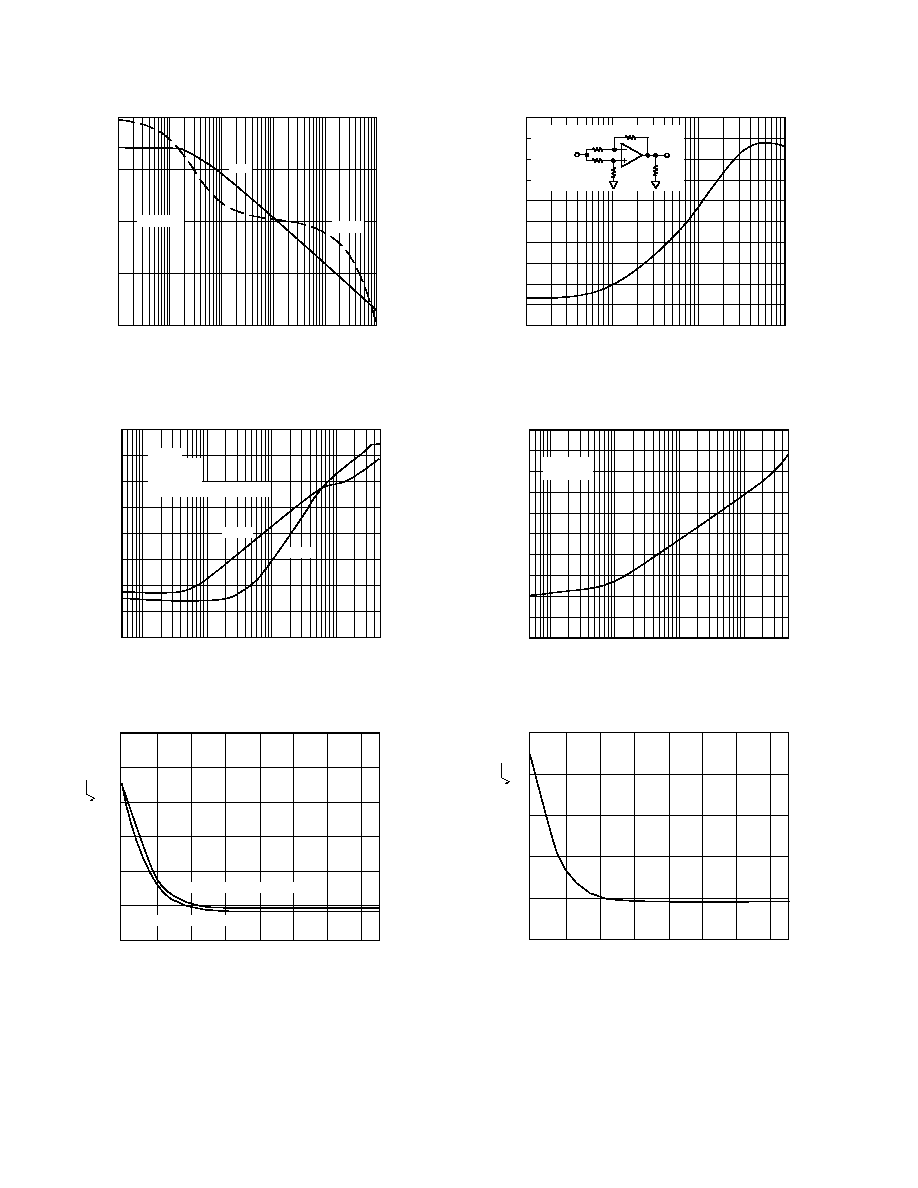
TRANSRESISTANCE
1M
100k
10k
1k
0.01
0.1
100
1
GAIN
PHASE
R
L
= 100
1000
10
PHASE
Degrees
0
40
80
120
FREQUENCY MHz
160
100
Figure 16. Transresistance and Phase vs. Frequency
FREQUENCY MHz
0.03 0.1
100
10
10
0
10
20
30
40
50
60
70
1
500
PSRR
dB
G = +2
R
F
= 301
R
L
= 100
100mV pp ON TOP OF V
S
PSRR
+PSRR
Figure 17. PSRR vs. Frequency
FREQUENCY Hz
300
0
10
100
250M
1k
10k
100k
1M
10M
100M
250
200
150
100
50
NONINVERTING CURRENT
INVERTING CURRENT
INPUT CURRENT
pA
Hz
Figure 18. Current Noise vs. Frequency
15
20
25
30
35
40
45
50
55
60
10
CMRR
dB
100
1
1000
10
FREQUENCY MHz
V
IN
=
200mVpp
100
V
O
301
154
301
154
Figure 19. CMRR vs. Frequency
100
10
1
0.1
0.01
0.03 0.1
100
10
1
500
OUTPUT RESISTANCE
FREQUENCY MHz
G = +2
R
F
= 301
Figure 20. Output Resistance vs. Frequency
INPUT VOLTAGE NOISE
nV
Hz
0
10
8
6
4
2
FREQUENCY Hz
10
100
250M
1k
10k
100k
1M
10M
100M
Figure 21. Voltage Noise vs. Frequency
AD8009
7
REV. D
SOURCE RESISTANCE
NOISE FIGURE
dB
25
20
15
10
5
0
100
10
1
500
G = +10
R
F
= 301
R
L
= 100
Figure 22. Noise Figure
FREQUENCY MHz
VSWR
0.1
1
100
10
2.0
1.8
1.6
1.4
1.2
1
0
500
Figure 23. Input VSWR; G = +10
250
20
18
0
16
14
12
10
8
6
4
2
P
OUT
MAX
dBm
FREQUENCY MHz
5
100
10
R
F
P
OUT
R
G
50
50
50
G = +2
R
F
= 301
G = +10
R
F
= 200
Figure 24. Maximum Output Power vs. Frequency
70
80
90
60
50
40
30
20
S
12
dB
100
1
1000
10
FREQUENCY MHz
G = +10
R
F
= 200
Figure 25. Reverse Isolation (S
12
); G = +10
VSWR
2.0
1.8
1.6
1.4
1.2
1
0
2.2
FREQUENCY MHz
0.1
1
100
10
C
COMP
= 0pF
C
COMP
= 3pF
200
49.9
C
COMP
49.9
22.1
500
Figure 26. Output VSWR; G = +10
10
0%
100
90
V
OUT
V
IN
= 2V
STEP
250ns
2V
2V
G = +10
R
F
= 200
R
L
= 100
Figure 27. Overdrive Recovery; G = +10
AD8009
8
REV. D
1ns
50mV
G = +2
R
F
= 301
R
L
= 150
V
O
= 200mV pp
Figure 28. Small Signal Transient Response; G = +2
1ns
500mV
G = +2
R
F
= 301
R
L
= 150
V
O
= 2V pp
Figure 29. 2 V Transient Response; G = +2
1.5ns
1V
G = +2
R
F
= 301
R
L
= 150
V
O
= 4V pp
Figure 30. 4 V Transient Response; G = +2
2ns
50mV
G = +10
R
F
= 200
R
L
= 100
V
O
= 200mV pp
Figure 31. Small Signal Transient Response; G = +10
2ns
500mV
G = +10
R
F
= 200
R
L
= 100
V
O
= 2V pp
Figure 32. 2 V Transient Response; G = +10
3ns
1V
G = +10
R
F
= 200
R
L
= 100
V
O
= 4V pp
Figure 33. 4 V Transient Response; G = +10
AD8009
9
REV. D
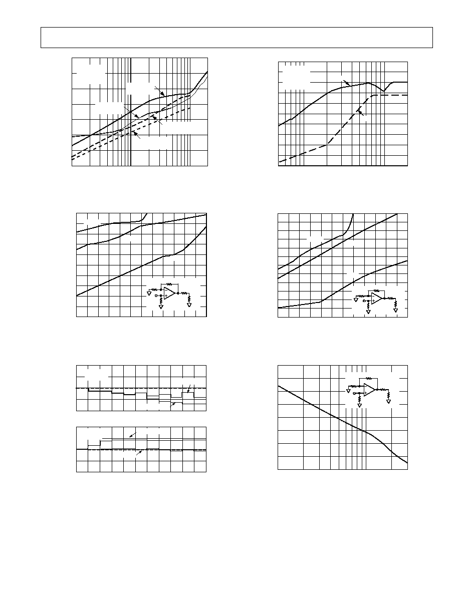
FREQUENCY MHz
10
1000
100
GAIN
dB
8
7
6
5
4
1
3
2
1
0
12
9
6
3
0
15
12
9
6
3
GAIN
dB
50
V
IN
C
A
499
V
OUT
= 200mV pp
V
OUT
499
100
C
A
= 0pF
1 dB/div
C
A
= 1pF
1 dB/div
C
A
= 2pF
3 dB/div
1
Figure 34. Small Signal Frequency Response vs. Parasitic
Capacitance
1.5ns
40mV
V
OUT
= 200mV pp
V
S
= 5V
C
A
= 2pF
C
A
= 1pF
C
A
= 0pF
499
100
50
V
OUT
V
IN
C
A
499
Figure 35. Small Signal Pulse Response vs. Parasitic
Capacitance
10 F
AD8009
HP8753D
49.9
301
49.9
+5V
5V
301
2
10 F
+
Z
OUT
= 50
Z
IN
= 50
+
0.001 F
0.1 F
0.001 F
0.1 F
3
7
4
6
WAVETEK 5201
BPF
Figure 36. AD8009 Driving a Bandpass RF Filter
CENTER 50.000 MHz
SPAN 80.000 MHz
0
10
20
30
40
50
60
70
80
90
REJECTION
dB
AD8009
G = 2
R
F
= R
G
= 301
DRIVING
WAVETEK 5201
TUNABLE BPF
f
C
= 50MHz
Figure 37. Frequency Response of Bandpass Filter Circuit
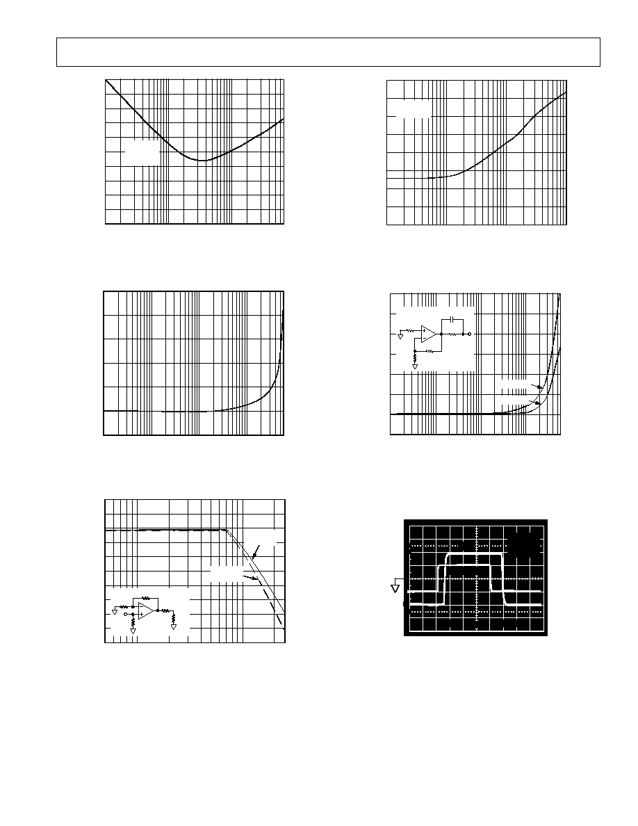
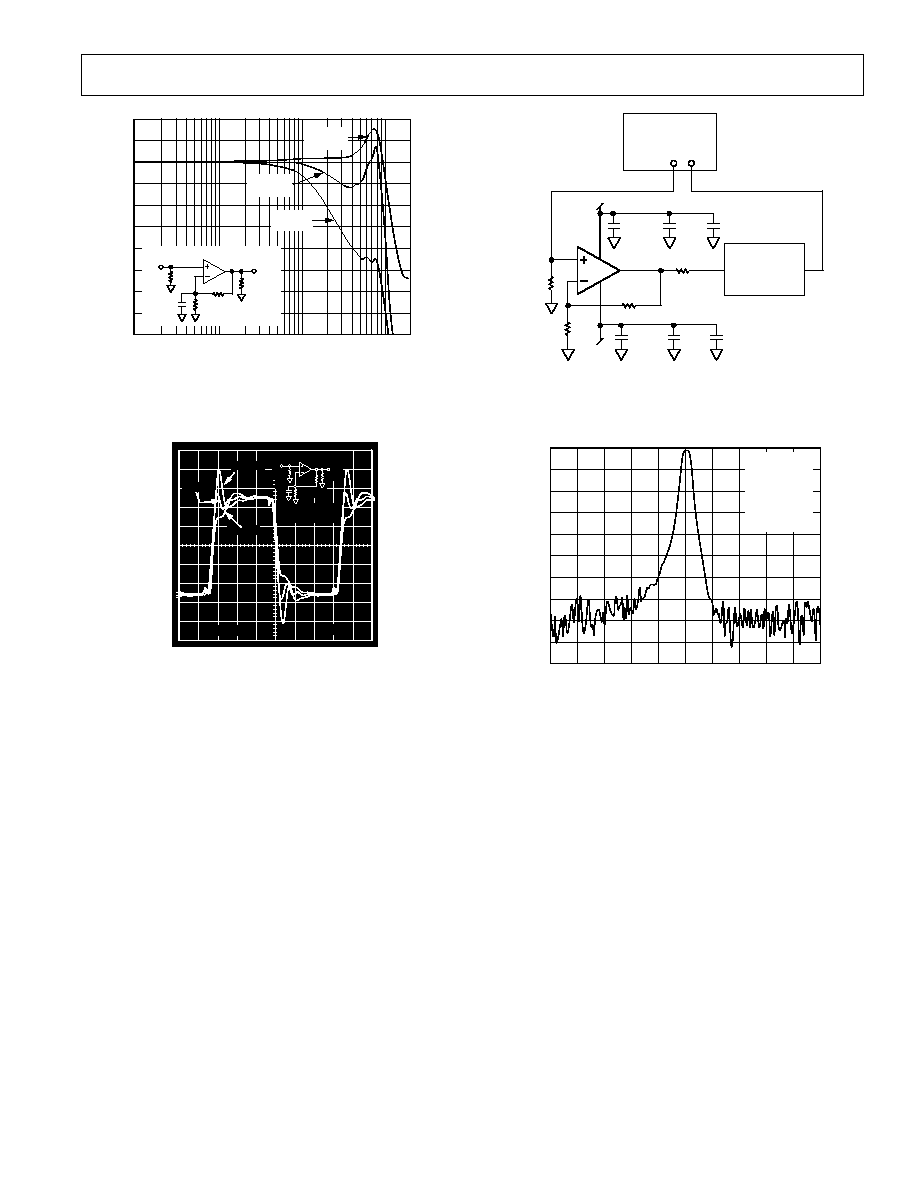
APPLICATIONS
All current feedback op amps are affected by stray capacitance
on their INPUT. Figures 34 and 35 illustrate the AD8009's
response to such capacitance.
Figure 34 shows the bandwidth can be extended by placing a
capacitor in parallel with the gain resistor. The small signal pulse
response corresponding to such an increase in capacitance/
bandwidth is shown in Figure 35.
As a practical consideration, the higher the capacitance on the
INPUT to GND, the higher R
F
needs to be to minimize
peaking/ringing.
RF Filter Driver
The output drive capability, wide bandwidth and low distortion
of the AD8009 are well suited for creating gain blocks that can
drive RF filters. Many of these filters require that the input be
driven by a 50
source, while the output must be terminated in
50
for the filters to exhibit their specified frequency response.
Figure 36 shows a circuit for driving and measuring the
frequency response of a filter, a Wavetek 5201 Tunable Band
Pass Filter that is tuned to a 50 MHz center frequency. The
HP8753D network provides a stimulus signal for the measure-
ment. The analyzer has a 50
source impedance that drives a
cable that is terminated in 50
at the high impedance nonin-
verting input of the AD8009.
The AD8009 is set at a gain of two. The series 50
resistor at
the output, along with the 50
termination provided by the
filter and its termination, yield an overall unity gain for the
measured path. The frequency response plot of Figure 37
shows the circuit to have an insertion loss of 1.3 dB in the pass
band and about 75 dB rejection in the stop band.
AD8009
10
REV. D
10 F
+
0.1 F
AD8009
75
301
5V
301
2
7
3
6
+
10 F
0.1 F
4
5V
AD8009
75
301
301
2
3
6
AD8009
75
301
301
2
3
6
75
75
75
75 COAX
PRIMARY MONITOR
ADDITIONAL MONITOR
75 COAX
75
75
75
75
75
75
RED
GREEN
BLUE
RED
GREEN
BLUE
I
OUT
R
ADV7160
ADV7162
I
OUT
G
I
OUT
B
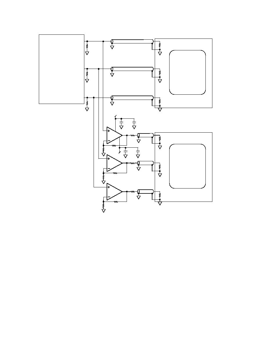
Figure 38. Driving an Additional High Resolution Monitor Using Three AD8009s
RGB Monitor Driver
High resolution computer monitors require very high full power
bandwidth signals to maximize their display resolution. The
RGB signals that drive these monitors are generally provided by
a current-out RAMDAC that can directly drive a 75
doubly
terminated line.
There are times when the same output wants to be delivered to
additional monitors. The termination provided internally by
each monitor prohibits the ability to simply connect a second
monitor in parallel with the first. Additional buffering must be
provided.
Figure 38 shows a connection diagram for two high resolution
monitors being driven by an ADV7160 or ADV7162, a 220 MHz
(Mega-pixel per second) triple RAMDAC. This pixel rate
requires a driver whose full power bandwidth is at least half the
pixel rate or 110 MHz. This is to provide good resolution for a
worst case signal that swings between zero scale and full scale
on adjacent pixels.
The primary monitor is connected in the conventional fashion
with a 75
termination to ground at each end of the 75
cable. Sometimes this configuration is called "doubly termi-
nated" and is used when the driver is a high output impedance
current source.
For the additional monitor, each of the RGB signals close to the
RAMDAC output is applied to a high input impedance, noninvert-
ing input of an AD8009 that is configured for a gain of +2. The
outputs each drive a series 75
resistor, cable and termination
resistor in the monitor that divides the output signal by two, thus
providing an overall unity gain. This scheme is referred to as
"back termination" and is used when the driver is a low output
impedance voltage source. Back termination requires that the
voltage of the signal be double the value that the monitor sees.
Double termination requires that the output current be double the
value that flows in the monitor termination.
AD8009
11
REV. D
Driving a Capacitive Load
A capacitive load, like that presented by some A/D converters,
can sometimes be a challenge for an op amp to drive depending
on the architecture of the op amp. Most of the problem is
caused by the pole created by the output impedance of the op
amp and the capacitor that is driven. This creates extra phase
shift that can eventually cause the op amp to become unstable.
One way to prevent instability and improve settling time when
driving a capacitor is to insert a resistor in series between the op
amp output and the capacitor. The feedback resistor is still
connected directly to the output of the op amp, while the series
resistor provides some isolation of the capacitive load from the
op amp output.
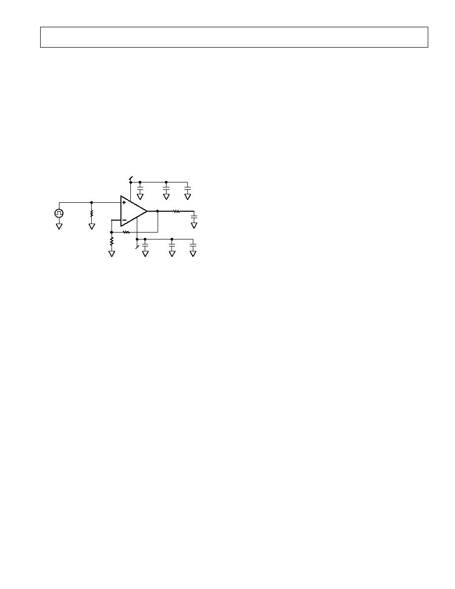
10 F
+
0.1 F
0.001 F
10 F
+
0.1 F
0.001 F
AD8009
49.9
+5V
5V
3
2
4
R
T
R
S
C
L
50pF
2V
STEP
7
6
R
F
R
G
G = + 2: R
F
= 301 = R
G
G = + 10: R
F
= 200 , R
G
= 22.1
Figure 39. Capacitive Load Drive Circuit
Figure 39 shows such a circuit with an AD8009 driving a 50 pF
load. With R
S
= 0, the AD8009 circuit will be unstable. For a
gain of +2 and +10, it was found experimentally that setting R
S
to 42.2
will minimize the 0.1% settling time with a 2 V step at
the output. The 0.1% settling time was measured to be 40 ns with
this circuit.
For smaller capacitive loads, a smaller R
S
will yield optimal
settling time, while a larger R
S
will be required for larger capacitive
loads. Of course, a larger capacitance will always require more
time for settling to a given accuracy than a smaller one, and this
will be lengthened by the increase in R
S
required. At best, a given
RC combination will require about 7 time constants by itself to
settle to 0.1%, so a limit will be reached where too large a
capacitance cannot be driven by a given op amp and still
meet the system's required settling time specification.
AD8009
12
REV. D
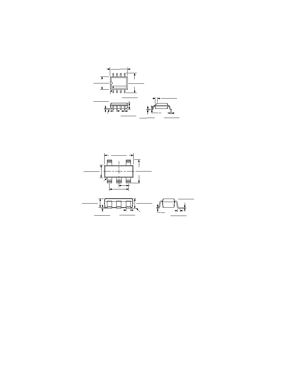
OUTLINE DIMENSIONS
Dimensions shown in inches and (mm).
C01011a010/00 (rev. D)
PRINTED IN U.S.A.
8-Lead SOIC
(SO-8)
0.1968 (5.00)
0.1890 (4.80)
8
5
4
1
0.2440 (6.20)
0.2284 (5.80)
PIN 1
0.1574 (4.00)
0.1497 (3.80)
0.0688 (1.75)
0.0532 (1.35)
SEATING
PLANE
0.0098 (0.25)
0.0040 (0.10)
0.0192 (0.49)
0.0138 (0.35)
0.0500
(1.27)
BSC
0.0098 (0.25)
0.0075 (0.19)
0.0500 (1.27)
0.0160 (0.41)
8
°
0
°
0.0196 (0.50)
0.0099 (0.25)
x 45
°
5-Lead Plastic Surface Mount (SOT-23)
(RT-5)
0.1181 (3.00)
0.1102 (2.80)
PIN 1
0.0669 (1.70)
0.0590 (1.50)
0.1181 (3.00)
0.1024 (2.60)
1
3
4
5
0.0748 (1.90)
BSC
0.0374 (0.95) BSC
2
0.0079 (0.20)
0.0031 (0.08)
0.0217 (0.55)
0.0138 (0.35)
10
0
0.0197 (0.50)
0.0138 (0.35)
0.0059 (0.15)
0.0019 (0.05)
0.0512 (1.30)
0.0354 (0.90)
SEATING
PLANE
0.0571 (1.45)
0.0374 (0.95)