 | ÐлекÑÑоннÑй компоненÑ: AD8012 | СкаÑаÑÑ:  PDF PDF  ZIP ZIP |
Äîêóìåíòàöèÿ è îïèñàíèÿ www.docs.chipfind.ru
REV. A
Information furnished by Analog Devices is believed to be accurate and
reliable. However, no responsibility is assumed by Analog Devices for its
use, nor for any infringements of patents or other rights of third parties
which may result from its use. No license is granted by implication or
otherwise under any patent or patent rights of Analog Devices.
a
AD8012
One Technology Way, P.O. Box 9106, Norwood, MA 02062-9106, U.S.A.
Tel: 781/329-4700
World Wide Web Site: http://www.analog.com
Fax: 781/326-8703
© Analog Devices, Inc., 1999
Dual 350 MHz
Low Power Amplifier
FUNCTIONAL BLOCK DIAGRAM
8
7
6
5
1
2
3
4
OUT1
IN1
+IN1
+V
S
OUT2
IN2
+IN2
V
S
AD8012
FEATURES
Low Power
1.7 mA/Amplifier Supply Current
Fully Specified for 5 V and +5 V Supplies
High Output Current, 125 mA
High Speed
350 MHz, 3 dB Bandwidth (G = +1)
150 MHz, 3 dB Bandwidth (G = +2)
2,250 V/ s Slew Rate
20 ns Settling Time to 0.1%
Low Distortion
72 dBc Worst Harmonic @ 500 kHz, R
L
= 100
66 dBc Worst Harmonic @ 5 MHz, R
L
= 1 k
Good Video Specifications (R
L
= 1 k , G = +2)
0.02% Differential Gain Error
0.06 Differential Phase Error
Gain Flatness 0.1 dB to 40 MHz
60 ns Overdrive Recovery
Low Offset Voltage, 1.5 mV
Low Voltage Noise, 2.5 nV/
Hz
Available in 8-Lead SOIC and 8-Lead microSOIC
APPLICATIONS
XDSL, HDSL Line Driver
ADC Buffer
Professional Cameras
CCD Imaging System
Ultrasound Equipment
Digital Camera
PRODUCT DESCRIPTION
The AD8012 is a dual low power current feedback amplifier
capable of providing 350 MHz bandwidth while using only
1.7 mA per amplifier. It is intended for use in high frequency,
wide dynamic range systems where low distortion, high speed
are essential and low power is critical.
With only 1.7 mA of supply current, the AD8012 also offers
exceptional ac specs such as 20 ns settling time and 2,250 V/
µ
s
slew rate. The video specifications are 0.02% differential gain
and 0.06 degree differential phase, excellent for such a low power
amplifier. In addition, the AD8012 has a low offset of 1.5 mV.
The AD8012 is well suited for any application that requires high
performance with minimal power.
The product is available in standard 8-lead SOIC or micro-
SOIC packages and operates over the industrial temperature
range 40
°
C to +85
°
C.
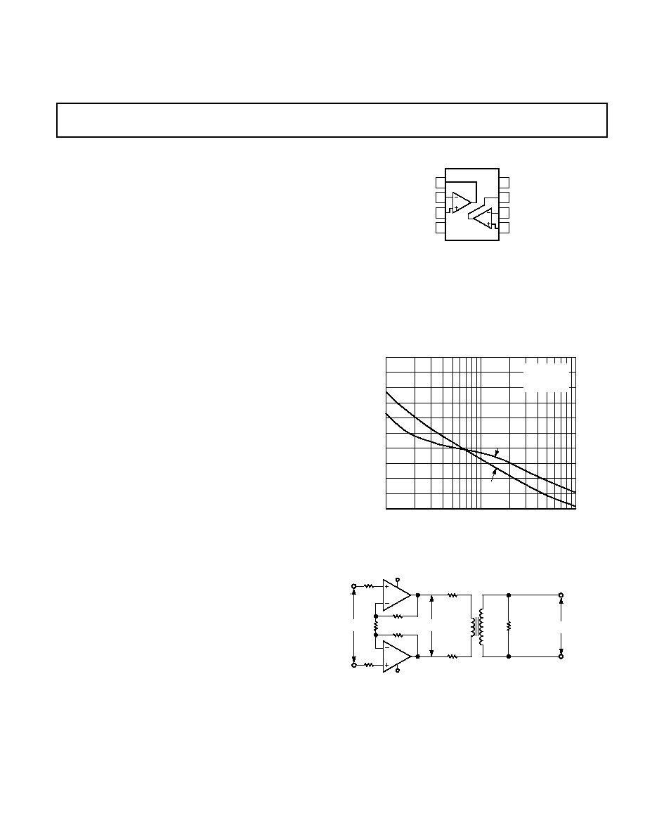
R
L
40
90
10
1k
100
DISTORTION dBc
70
80
60
50
G = +2
V
OUT
= 2V p-p
R
F
= 750
3rd
2nd
Figure 1. Distortion vs. Load Resistance, V
S
=
±
5 V,
Frequency = 500 kHz
AMP 1
V
IN
V
REF
R2
R1
R
L
= 100
OR
135
V
OUT
Np:Ns
TRANSFORMER
LINE
POWER
IN dB
+V
S
+
V
S
+
Figure 2. Differential Drive Circuit for XDSL Applications
*
*Protected under U.S. Patent Number 5,537,079.

2
REV. A
AD8012SPECIFICATIONS
DUAL SUPPLY
Parameter
Conditions
Min
Typ
Max
Units
DYNAMIC PERFORMANCE
3 dB Small Signal Bandwidth
G = +1, V
OUT
< 0.4 V p-p, R
L
= 1 k
270
350
MHz
G = +2, V
OUT
< 0.4 V p-p, R
L
= 1 k
95
150
MHz
G = +2, V
OUT
< 0.4 V p-p, R
L
= 100
90
MHz
0.1 dB Bandwidth
V
OUT
< 0.4 V p-p, R
L
= 1 k
/100
40/23
MHz
Large Signal Bandwidth
V
OUT
= 4 V p-p
75
MHz
Slew Rate
V
OUT
= 4 V p-p
2,250
V/
µ
s
Rise and Fall Time
V
OUT
= 2 V p-p
3
ns
Settling Time
0.1%, V
OUT
= 2 V p-p
20
ns
0.02%, V
OUT
= 2 V p-p
35
ns
Overdrive Recovery
2
×
Overdrive
60
ns
NOISE/HARMONIC PERFORMANCE
Distortion
V
OUT
= 2 V p-p, G = +2
2nd Harmonic
500 kHz, R
L
= 1 k
/100
89/73
dBc
5 MHz, R
L
= 1 k
/100
78/62
dBc
3rd Harmonic
500 kHz, R
L
= 1 k
/100
84/72
dBc
5 MHz, R
L
= 1 k
/100
66/52
dBc
Output IP3
500 kHz,
f = 10 kHz, R
L
= 1 k
/100
30/40
dBm
IMD
500 kHz,
f = 10 kHz, R
L
= 1 k
/100
79/77
dBc
Crosstalk
5 MHz, R
L
= 100
70
dB
Input Voltage Noise
f = 10 kHz
2.5
nV/
Hz
Input Current Noise
f = 10 kHz, +Input, Input
15
pA/
Hz
Differential Gain
f = 3.58 MHz, R
L
= 150
/1 k
, G = +2
0.02/0.02
%
Differential Phase
f = 3.58 MHz, R
L
= 150
/1 k
, G = +2
0.3/0.06
Degrees
DC PERFORMANCE
Input Offset Voltage
±
1.5
±
4
mV
T
MIN
T
MAX
±
5
mV
Open-Loop Transimpedance
V
OUT
=
±
2 V, R
L
= 100
240
500
k
T
MIN
T
MAX
200
k
INPUT CHARACTERISTICS
Input Resistance
+Input
450
k
Input Capacitance
+Input
2.3
pF
Input Bias Current
+Input, Input
±
3
±
12
µ
A
+Input, Input, T
MIN
T
MAX
±
15
µ
A
Common-Mode Rejection Ratio
V
CM
=
±
2.5 V
56
60
dB
Input Common-Mode Voltage Range
±
3.8
±
4.1
V
OUTPUT CHARACTERISTICS
Output Resistance
G = +2
0.1
Output Voltage Swing
±
3.85
±
4
V
Output Current
T
MIN
T
MAX
70
125
mA
Short Circuit Current
500
mA
POWER SUPPLY
Supply Current/Amp
1.7
1.8
mA
T
MIN
T
MAX
1.9
mA
Operating Range
Dual Supply
±
1.5
±
6.0
V
Power Supply Rejection Ratio
58
60
dB
Specifications subject to change without notice.
(@ T
A
= +25 C, V
S
= 5 V, G = +2, R
L
= 100
, R
F
= R
G
= 750
, unless otherwise noted)

3
REV. A
AD8012
(@ T
A
+25 C, V
S
= +5 V, G = +2, R
L
= 100 , R
F
= R
G
= 750 , unless otherwise noted)
Parameter
Conditions
Min
Typ
Max
Units
DYNAMIC PERFORMANCE
3 dB Small Signal Bandwidth
G = +1, V
OUT
< 0.4 V p-p, R
L
= 1 k
220
300
MHz
G = +2, V
OUT
< 0.4 V p-p, R
L
= 1 k
90
140
MHz
G = +2, V
OUT
< 0.4 V p-p, R
L
= 100
85
MHz
0.1 dB Bandwidth
V
OUT
< 0.4 V p-p, R
L
= 1 k
/100
43/24
MHz
Large Signal Bandwidth
V
OUT
= 2 V p-p
60
MHz
Slew Rate
V
OUT
= 3 V p-p
1,200
V/
µ
s
Rise and Fall Time
V
OUT
= 2 V p-p
2
ns
Settling Time
0.1%, V
OUT
= 2 V p-p
25
ns
0.02%, V
OUT
= 2 V p-p
40
ns
Overdrive Recovery
2
×
Overdrive
60
ns
NOISE/HARMONIC PERFORMANCE
Distortion
V
OUT
= 2 V p-p, G = +2
2nd Harmonic
500 kHz, R
L
= 1 k
/100
87/71
dBc
5 MHz, R
L
= 1 k
/100
77/61
dBc
3rd Harmonic
500 kHz, R
L
= 1 k
/100
89/72
dBc
5 MHz, R
L
= 1 k
/100
78/52
dBc
Output IP3
500 kHz, R
L
= 1 k
/100
30/40
dBm
IMD
500 kHz, R
L
= 1 k
/100
77/80
dBc
Crosstalk
5 MHz, R
L
= 100
70
dB
Input Voltage Noise
f = 10 kHz
2.5
nV/
Hz
Input Current Noise
f = 10 kHz, +Input, Input
15
pA/
Hz
Black Level Clamped to +2 V, f = 3.58 MHz
Differential Gain
R
L
= 150
/1 k
0.03/0.03
%
Differential Phase
R
L
= 150
/1 k
0.4/0.08
Degrees
DC PERFORMANCE
Input Offset Voltage
±
1
±
3
mV
T
MIN
T
MAX
±
4
mV
Open-Loop Transimpedance
V
OUT
= 2 V p-p, R
L
= 100
200
400
k
T
MIN
T
MAX
150
k
INPUT CHARACTERISTICS
Input Resistance
+Input
450
k
Input Capacitance
+Input
2.3
pF
Input Bias Current
+Input, Input
±
3
±
12
µ
A
+Input, Input, T
MIN
T
MAX
±
15
µ
A
Common-Mode Rejection Ratio
V
CM
= 1.5 V to 3.5 V
56
60
dB
Input Common-Mode Voltage Range
1.5 to 3.5
1.2 to 3.8
V
OUTPUT CHARACTERISTICS
Output Resistance
G = +2
0.1
Output Voltage Swing
1 to 4
0.9 to 4.2
V
Output Current
T
MIN
T
MAX
50
100
mA
Short Circuit Current
500
mA
POWER SUPPLY
Supply Current/Amp
1.55
1.75
mA
T
MIN
T
MAX
1.85
mA
Operating Range
Single Supply
3
12
V
Power Supply Rejection Ratio
58
60
dB
Specifications subject to change without notice.
SINGLE SUPPLY
AD8012
4
REV. A
ABSOLUTE MAXIMUM RATINGS
1
Supply Voltage . . . . . . . . . . . . . . . . . . . . . . . . . . . . . . . 12.6 V
Internal Power Dissipation
2
Small Outline Package (R) . . . . . . . . . . . . . . . . . . . . . 0.8 W
microSOIC Package (RM) . . . . . . . . . . . . . . . . . . . . . 0.6 W
Input Voltage (Common Mode) . . . . . . . . . . . . . . . . . . .
±
V
S
Differential Input Voltage . . . . . . . . . . . . . . . . . . . . . .
±
2.5 V
Output Short Circuit Duration
. . . . . . . . . . . . . . . . . . . . . . Observe Power Derating Curves
Storage Temperature Range RM, R . . . . . . 65
°
C to +125
°
C
Operating Temperature Range (A Grade) . . 40
°
C to +85
°
C
Lead Temperature Range (Soldering 10 sec) . . . . . . . +300
°
C
NOTES
1
Stresses above those listed under Absolute Maximum Ratings may cause perma-
nent damage to the device. This is a stress rating only; functional operation of the
device at these or any other conditions above those indicated in the operational
section of this specification is not implied. Exposure to absolute maximum rating
conditions for extended periods may affect device reliability.
2
Specification is for device in free air at +25
°
C
8-Lead SOIC Package:
JA
= 155
°
C/W
8-Lead microSOIC Package:
JA
= 200
°
C/W
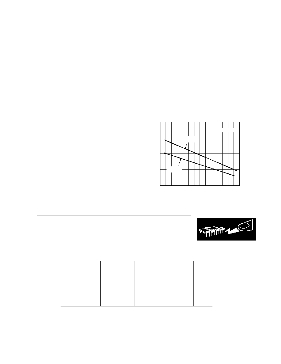
MAXIMUM POWER DISSIPATION
The maximum power that can be safely dissipated by the AD8012
is limited by the associated rise in junction temperature. The maxi-
mum safe junction temperature for plastic encapsulated devices
is determined by the glass transition temperature of the plastic,
approximately +150
°
C. Temporarily exceeding this limit may
cause a shift in parametric performance due to a change in the
stresses exerted on the die by the package. Exceeding a junction
temperature of +175
°
C for an extended period can result in de-
vice failure.
The output stage of the AD8012 is designed for maximum load
current capability. As a result, shorting the output to common
can cause the AD8012 to source or sink 500 mA. To ensure
proper operation, it is necessary to observe the maximum power
derating curves. Direct connection of the output to either power
supply rail can destroy the device.
AMBIENT TEMPERATURE C
50
0
T
J
= +150 C
2.0
1.5
1.0
MAXIMUM POWER DISSIPATION Watts
8-LEAD SOIC
PACKAGE
40 30
0
10
20
30
40
50
60
70
80 90
8-LEAD
microSOIC
0.5
20 10
Figure 3. Plot of Maximum Power Dissipation vs.
Temperature for AD8012
CAUTION
ESD (electrostatic discharge) sensitive device. Electrostatic charges as high as 4000 V readily
accumulate on the human body and test equipment and can discharge without detection.
Although the AD8012 features proprietary ESD protection circuitry, permanent damage may
occur on devices subjected to high energy electrostatic discharges. Therefore, proper ESD
precautions are recommended to avoid performance degradation or loss of functionality.
WARNING!
ESD SENSITIVE DEVICE
ORDERING GUIDE
Temperature
Package
Package
Brand
Model
Range
Description
Options
Code
AD8012AR
40
°
C to +85
°
C
8-Lead SOIC
SO-8
AD8012AR-REEL
40
°
C to +85
°
C
13
" Tape and Reel
SO-8
AD8012AR-REEL7
40
°
C to +85
°
C
7
" Tape and Reel
SO-8
AD8012ARM
40
°
C to +85
°
C
8-Lead microSOIC
RM-08
H6A
AD8012ARM-REEL
40
°
C to +85
°
C
13
" Tape and Reel
RM-08
H6A
AD8012ARM-REEL7
40
°
C to +85
°
C
7
" Tape and Reel
RM-08
H6A
AD8012
5
REV. A
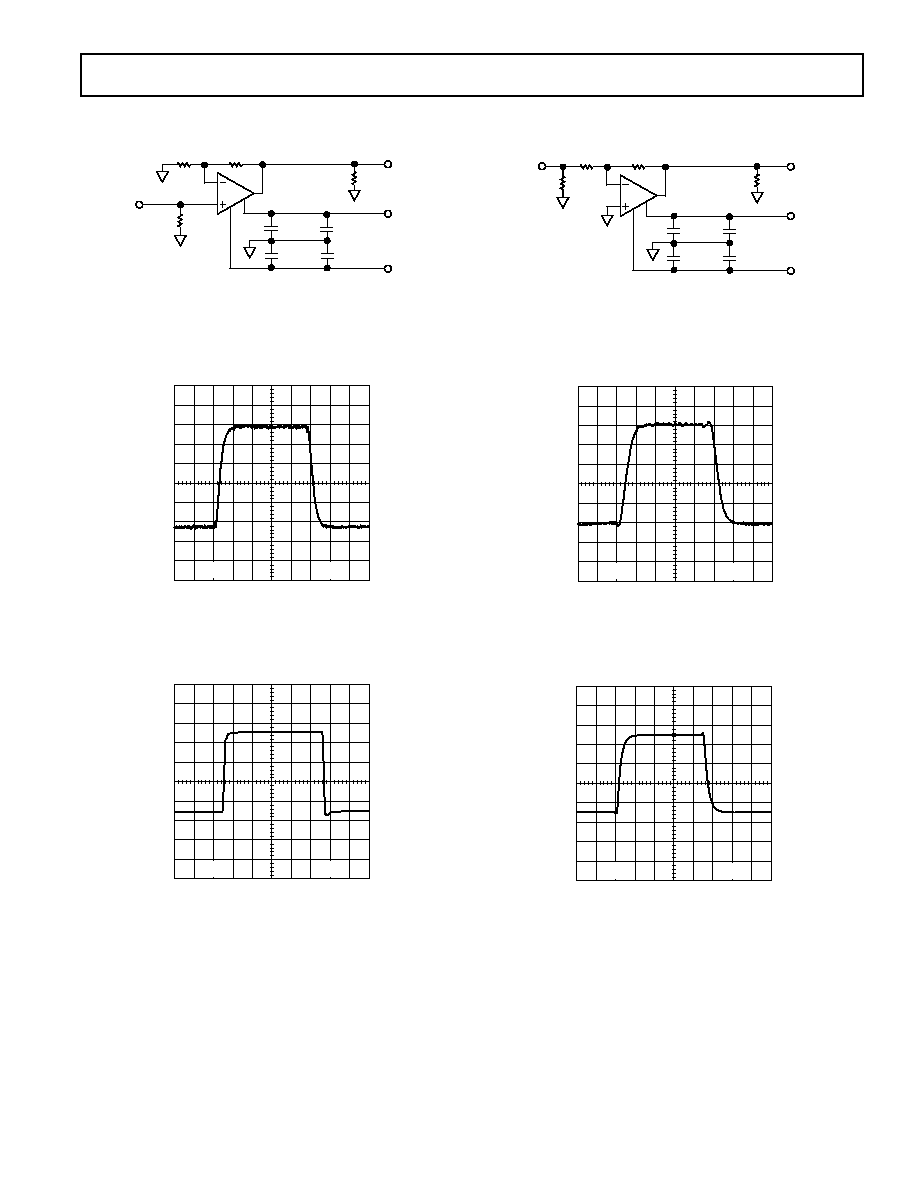
0.1 F
0.1 F
10 F
10 F
R
L
V
IN
V
OUT
750
750
49.9
+V
S
V
S
+
+
Figure 4. Test Circuit; Gain = +2
20mV
5ns
Figure 5.* 100 mV Step Response; G = +2, V
S
=
±
2.5 V or
±
5 V, R
L
= 1 k
1V
10ns
Figure 6. 4 V Step Response; G = +2, V
S
=
±
5 V, R
L
= 1 k
*NOTE: V
S
=
±
2.5 V operation is identical to V
S
= +5 V single supply operation.
0.1 F
0.1 F
10 F
10 F
R
L
V
IN
V
OUT
750
750
53.6
+V
S
V
S
+
+
Figure 7. Test Circuit; Gain = 1
20mV
5ns
Figure 8.* 100 mV Step Response; G = 1, V
S
=
±
2.5 V or
±
5 V, R
L
= 1 k
1V
10ns
Figure 9. 4 V Step Response; G = 1, V
S
=
±
5 V, R
L
= 1 k
Typical Performance Characteristics