 | ÐлекÑÑоннÑй компоненÑ: AD8018 | СкаÑаÑÑ:  PDF PDF  ZIP ZIP |
Äîêóìåíòàöèÿ è îïèñàíèÿ www.docs.chipfind.ru
REV. 0
Information furnished by Analog Devices is believed to be accurate and
reliable. However, no responsibility is assumed by Analog Devices for its
use, nor for any infringements of patents or other rights of third parties
which may result from its use. No license is granted by implication or
otherwise under any patent or patent rights of Analog Devices.
a
AD8018
One Technology Way, P.O. Box 9106, Norwood, MA 02062-9106, U.S.A.
Tel: 781/329-4700
World Wide Web Site: http://www.analog.com
Fax: 781/326-8703
© Analog Devices, Inc., 2000
5 V, Rail-to-Rail, High-Output Current,
xDSL Line Drive Amplifier
FEATURES
Ideal xDSL Line Drive Amplifier for USB, PCMCIA, or
PCI-Based Customer Premise Equipment (CPE). The
AD8018 provides maximum reach on 5 V supply,
driving 16 dBm of power into a back-terminated,
transformer-coupled 100 while maintaining 82 dBc
of out-of-band SFDR.
Rail-to-Rail Output Voltage and High Output Current
Drive
400 mA Output Current into Differential Load of 10
@ 8 V p-p
Low Single-Tone Distortion
86 dBc Worst Harmonic, 6 V p-p into Differential 10
@ 100 kHz
Low Noise
4.5 nV/
Hz Voltage Noise Density, 100 kHz
Out-of-Band SFDR = 82 dBc, 144 kHz to 500 kHz,
R
LOAD
= 12.5
, P
LINE
= 13 dBm
Low-Power Operation
3.3 V to 8 V Power Supply Range
Two Logic Bits for Standby and Shutdown
Low Supply Current of 9 mA/Amplifier (Typ)
Current Feedback Amplifiers
High Speed
130 MHz Bandwidth (3 dB)
300 V/ s Slew Rate
APPLICATIONS
xDSL USB, PCI, PCMCIA Cards
Consumer DSL Modems
Twisted Pair Line Driver
PRODUCT DESCRIPTION
The AD8018 is intended for use in single-supply (5 V) xDSL
modems where high-output current and low distortion are
essential to achieve maximum reach. The dual high-speed
amplifiers are capable of driving low distortion signals to within
0.5 V of the power supply rail. Each amplifier can drive 400 mA
of current into 10
(differential) while maintaining 82 dBc
out-of-band SFDR. The AD8018 is available with flexible standby
and shutdown modes. Two digital logic bits (PWDN1 and
PWDN0) may be used to put the AD8018 into one of three
modes: full power, standby (outputs low impedance), and
shutdown (outputs high impedance).
Fabricated with ADI's high-speed XFCB (eXtra Fast Comple-
mentary Bipolar) process, the high bandwidth and fast slew rate
of the AD8018 keep distortion to a minimum, while dissipat-
ing a minimum of power. The quiescent current of the AD8018
is a low 9 mA/amplifier. The AD8018 drive capability comes in
compact 8-lead Thermal Coastline SOIC and 14-lead TSSOP
packages. Low-distortion, rail-to-rail output voltage, and high-
current drive in small packages make the AD8018 ideal for use
in low-cost USB, PCMCIA, and PCI Customer Premise Equip-
ment for ADSL, SDSL, VDSL, and proprietary xDSL systems.
Both models will operate over the temperature range 40
°C to
+85
°C.
10
1nF
5V
750
V
IN
10
1nF
750
750
0.01 F
0.01 F
V
REF
0.01 F
100
100
10k
10k
P
OUT
16dBm
R1
3.1
R2
3.1
R
L
= 100
LINE-
POWER
13dBm
TRANSFORMER
1:4
10k
10k
Figure 2. Single-Supply Voltage Differential Drive Circuit
for xDSL Applications
8-Lead SOIC
(Thermal Coastline)
V
S
IN2
IN2
6
5
7
8
OUT2
OUT1
IN1
IN1
V
S
1
2
3
4
AD8018AR
PIN CONFIGURATIONS
14-Lead TSSOP
OUT1
IN1
IN1
V
S
PWDN1
V
S
OUT2
IN2
IN2
PWDN0
DGND
AD8018ARU
6
5
7
8
1
2
3
4
9
14
13
12
11
10
NC
NC
NC
NC = NO CONNECT
P
LINE
dBm
SFDR
dBc
70
80
90
60
50
40
30
4
18
6
8
10
12
14
16
N = 4.0
V
S
= 3.3V
V
S
= 5V
V
S
= 8V
Figure 1. Out-of-Band SFDR vs. ADSL Upstream Line Power;
V
S
= 5 V, N = 4 Turns, 144 kHz to 500 kHz. See Evaluation
Board Schematics in Figure 11.

REV. 0
2
AD8018SPECIFICATIONS
(@ 25 C, V
S
= 5 V, R
L
= 100
, R
F
= R
G
= 750
unless otherwise noted.)
Parameter
Conditions
Min
Typ
Max
Unit
DYNAMIC PERFORMANCE
3 dB Bandwidth
G = 1, V
OUT
< 0.4 V p-p, R
L
= 5
40
50
MHz
G = 1, V
OUT
< 0.4 V p-p, R
L
= 100
100
130
MHz
G = 2, V
OUT
< 0.4 V p-p, R
L
= 5
35
40
MHz
G = 2, V
OUT
< 0.4 V p-p, R
L
= 100
80
100
MHz
0.1 dB Bandwidth
V
OUT
< 0.4 V p-p, R
L
= 100
10
MHz
Large Signal Bandwidth
V
OUT
= 4 V p-p, G = +2
80
MHz
Slew Rate
Noninverting, V
OUT
= 4 V p-p
300
V/ s
Rise and Fall Time
Noninverting, V
OUT
= 2 V p-p
5.5
ns
Settling Time
0.1%, V
OUT
= 2 V p-p, R
L
= 100
25
ns
NOISE/HARMONIC
PERFORMANCE
Distortion,
V
OUT
= 6 V p-p (Differential)
Second Harmonic
100 kHz, R
L
= 10
89
94
dBc
500 kHz, R
L
= 10
61
63
dBc
Third Harmonic
100 kHz, R
L
= 10
86
89
dBc
500 kHz, R
L
= 10
74
77
dBc
MTPR (In-Band)
25 kHz to 138 kHz, R
L
= 12.5
, P
LINE
= +13 dBm
70
dBc
SFDR (Out-of-Band)
144 kHz to 500 kHz, R
L
= 12.5
, P
LINE
= +13 dBm
82
dBc
Input Noise Voltage
f = 100 kHz
4.5
5
nV
Hz
Input Noise Current
f = 100 kHz (+Inputs)
1
pA
Hz
f = 100 kHz (Inputs)
10
pA
Hz
Crosstalk
f = 1 MHz, G = +2
74
dB
DC PERFORMANCE
Input Offset Voltage
1
15
mV
T
MIN
to T
MAX
17
mV
Input Offset Voltage Match
0.1
2.6
mV
Transimpedance
V
OUT
= 2 V p-p, R
L
= 5
830
2000
k
T
MIN
to T
MAX
700
k
INPUT CHARACTERISTICS
Input Resistance
+Input
10
M
Input
125
Input Capacitance
+Input
1
pF
Input Bias Current ()
0.3
8
A
T
MIN
to T
MAX
14
A
Input Bias Current () Match
0.1
5.5
A
T
MIN
to T
MAX
8
A
Input Bias Current (+)
1
1.5
A
T
MIN
to T
MAX
2.5
A
Input Bias Current (+) Match
0.1
0.5
A
T
MIN
to T
MAX
1
A
CMRR
V
IN
2 V to 4 V
51
54
dB
Input CM Voltage Range
1.2
3.8
V
OUTPUT CHARACTERISTICS
Cap Load
30% Overshoot
1000
pF
Output Resistance
Frequency = 100 kHz, PWDN1, PWDN0 = 1
0.2
Output Voltage Swing
R
L
= 100
0.16 to 4.87
V
R
L
= 5
0.5 to 4.5
V
Linear Output Current
SFDR < 85 dBc, f = 100 kHz, R
L
= 10
350
400
mA
Short-Circuit Current
1000
mA
POWER SUPPLY
Supply Current/Amp
PWDN1 = 1, PWDN0 = 1
9
10
mA
T
MIN
to T
MAX
11.4
mA
STBY Supply Current/Amp
PWDN1 = 0, PWDN0 = 1 or
4.5
5.1
mA
PWDN1 = 1, PWDN0 = 0
4.5
5.1
mA
SHUTDOWN Supply Current/Amp
PWDN1 = 0, PWDN0 = 0
0.3
0.55
mA
Operating Range
Single Supply
3.3
8
V
+Power Supply Rejection Ratio
V
S
= 1 V
60
66
dB
T
MIN
to T
MAX
56
dB
Power Supply Rejection Ratio
V
S
= 1 V
52
55
dB
T
MIN
to T
MAX
50
dB
REV. 0
3
AD8018
Parameter
Conditions
Min
Typ
Max
Unit
LOGIC INPUTS (PWDN1, 0)
Logic "1" Voltage
2.0
V
Logic "0" Voltage
0.8
V
Logic Input Bias Current
240
A
Standby Recovery Time
R
L
= 10
, G = +2, I
S
= 90% of Typical
500
ns
Specifications subject to change without notice.
ORDERING GUIDE
Temperature
Package
Package
Model
Range
Description
Option
AD8018AR
40
°C to +85°C 8-Lead Plastic
SO-8
SOIC
AD8018ARREEL
40
°C to +85°C 8-Lead SOIC
SO-8
AD8018ARU
40
°C to +85°C 14-Lead Plastic RU-14
TSSOP
AD8018ARUREEL 40
°C to +85°C 14-Lead Plastic RU-14
TSSOP
AD8018ARUEVAL
Evaluation Board RU-14
ABSOLUTE MAXIMUM RATINGS
1
Supply Voltage . . . . . . . . . . . . . . . . . . . . . . . . . . . . . . . . . . . 8 V
Internal Power Dissipation
2
Small Outline Package (R) . . . . . . . . . . . . . . . . . . . 650 mW
TSSOP Package (RU) . . . . . . . . . . . . . . . . . . . . . . 565 mW
Input Voltage (Common-Mode) . . . . . . . . . . . . . . . . . . . .
±V
S
Logic Voltage, PWDN0, 1 . . . . . . . . . . . . . . . . . . . . . . . . .
±V
S
Differential Input Voltage . . . . . . . . . . . . . . . . . . . . . . .
±1.6 V
Output Short Circuit Duration
. . . . . . . . . . . . . . . . . . . . . . Observe Power Derating Curves
Storage Temperature Range RU, R . . . . . . . 65
°C to +125°C
Operating Temperature Range . . . . . . . . . . . 40
°C to +85°C
Lead Temperature Range (Soldering 10 sec) . . . . . . . . . 300
°C
NOTES
1
Stresses above those listed under Absolute Maximum Ratings may cause perma-
nent damage to the device. This is a stress rating only; functional operation of the
device at these or any other conditions above those indicated in the operational
section of this specification is not implied. Exposure to absolute maximum rating
conditions for extended periods may affect device reliability.
2
Specification is for the device in free air:
8-Lead SOIC Package:
JA
= 100
°C/W.
8-Lead TSSOP Package:
JA
= 115
°C/W.
MAXIMUM POWER DISSIPATION
The maximum power that can be safely dissipated by the AD8018
is limited by the associated rise in junction temperature. The
maximum safe junction temperature for plastic encapsulated
devices is determined by the glass transition temperature of the
plastic, approximately 150
°C. Temporarily exceeding this limit
may cause a shift in parametric performance due to a change
in the stresses exerted on the die by the package. Exceeding a
junction temperature of 175
°C for an extended period can result
in device failure.
While the AD8018 is internally short circuit protected, this may
not be sufficient to guarantee that the maximum junction tempera-
ture (150
°C) is not exceeded under all conditions. To ensure
proper operation, it is necessary to observe the maximum power
derating curves.
AMBIENT TEMPERATURE C
2.0
50
MAXIMUM POWER DISSIPATION
Watts
1.5
1.0
0.5
0
40 30 20 10 0
10
20 30
40 50
60 70
80 90
T
J
= 150 C
14-LEAD TSSOP PACKAGE
8-LEAD SOIC PACKAGE
Figure 3. Plot of Maximum Power Dissipation vs.
Temperature
CAUTION
ESD (electrostatic discharge) sensitive device. Electrostatic charges as high as 4000 V readily
accumulate on the human body and test equipment and can discharge without detection. Although
the AD8018 features proprietary ESD protection circuitry, permanent damage may occur on
devices subjected to high-energy electrostatic discharges. Therefore, proper ESD precautions are
recommended to avoid performance degradation or loss of functionality.
WARNING!
ESD SENSITIVE DEVICE
REV. 0
AD8018
4
AD8018
V
S
V
SIGNAL
50
750
750
V
S
R
LOAD
V
OUT
10 F
TANT
10 F
TANT
0.1 F
0.1 F
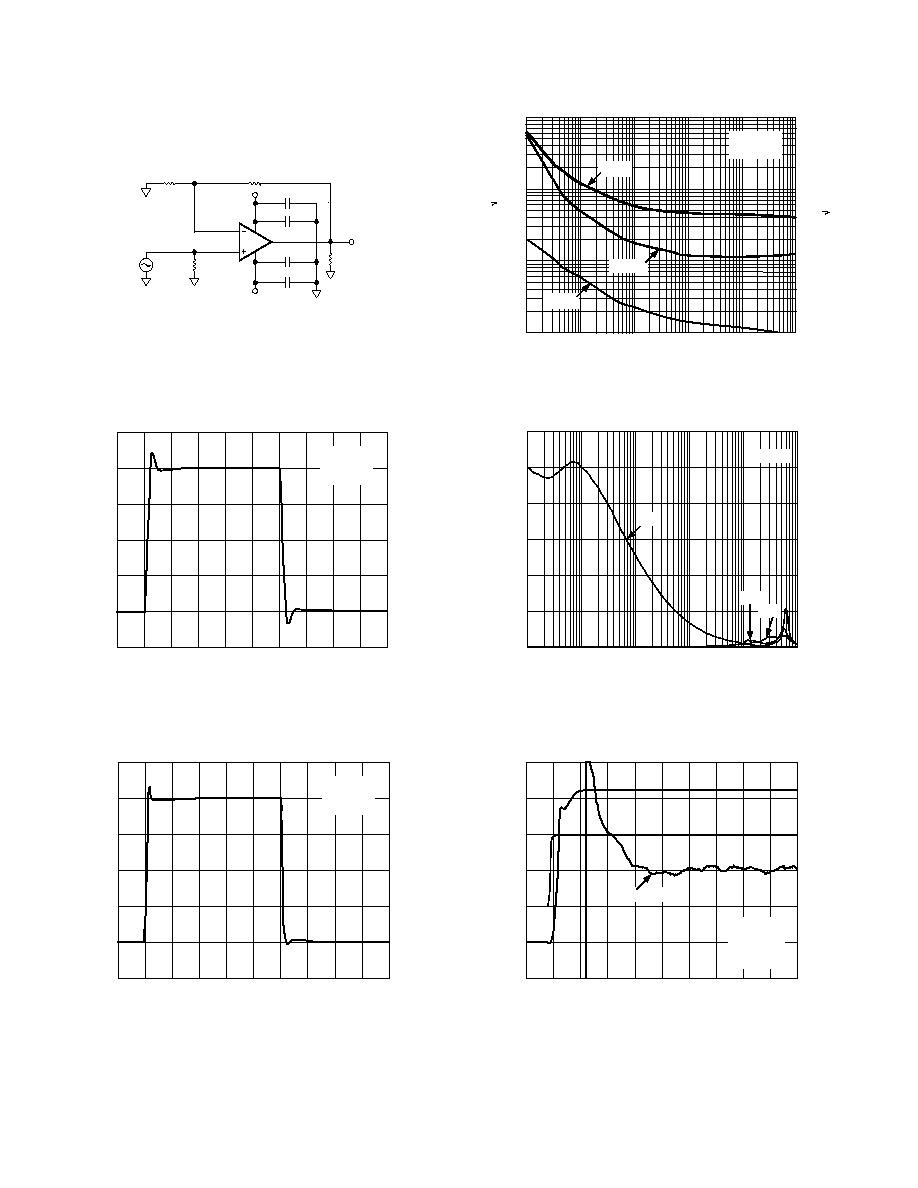
TPC 1. Single-Ended Test Circuit
TIME ns
0
OUTPUT VOLTAGE
mV
50
100
150
50
100
0
50
100
150
G = 2
V
S
= 2.5V
R
L
= 5
150
200
250
300
350
400
450
500
TPC 2. Small Signal Step Response
TIME ns
0
OUTPUT VOLTAGE
V
1
2
3
50
100
0
1
2
3
G = 2
V
S
= 2.5V
R
L
= 5
150
200
250
300
350
400
450
500
TPC 3. Large Signal Step Response
Typical Performance Characteristics
1
FREQUENCY Hz
10
10
1
100
1000
100
1k
10k
100k
1M
0.1
10
100
V
S
= 2.5V
R
L
= 100
V
NOISE
I
NOISE
I
NOISE
V
NOISE
nV/
Hz
(RTI)
I
NOISE
pA/
Hz
TPC 4. I
NOISE
and V
NOISE
vs. Frequency
FREQUENCY MHz
0.01
OUTPUT IMPEDANCE
500
0
2k
2.5k
3k
(1,1)
(0,0)
1.5k
1k
0.1
1
10
100
1k
(1,0)
V
S
= 2.5V
TPC 5. Output Impedance vs. Frequency, for Full Power,
Standby, and Shutdown Modes
mV
1
2
3
1
2
3
0
G = 2
V
S
= 2.5
V
IN
= 2V p-p
R
L
= 100
0
10
20
30
40
50
60
70
80
100
90
TIME ns
V
OUT
(V
IN
2)
(0.1%)
(+0.1%)
TPC 6. 0.1% Settling Time
REV. 0
AD8018
5
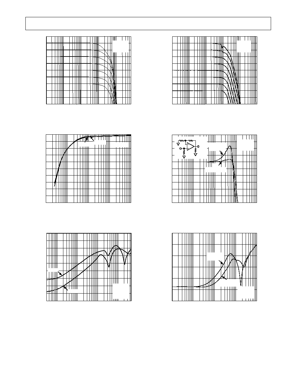
FREQUENCY Hz
10k
OUTPUT VOLTAGE
dBv
25
1M
5
10M
100M
1G
100k
22
19
16
13
10
7
4
1
2
G = 2
V
S
= 2.5V
R
L
= 100
TPC 7. Output Voltage vs. Frequency
LOAD RESISTANCE
1
OUTPUT SWING
Volts
1.9
1.7
1.5
10
2.1
2.5
100
1000
10k
1.6
1.8
2.0
2.2
2.3
2.4
SWING
SWING
V
S
= 2.5V
TPC 8. Output Swing vs. R
LOAD
FREQUENCY Hz
100k
PSRR
dB
70
90
1M
10M
100M
80
60
50
40
30
20
10
0
G = 2
V
S
= 2.5V
V
S
= 1V
R
L
= 100
PSRR
PSRR
TPC 9. PSRR vs. Frequency
FREQUENCY Hz
10k
OUTPUT VOLTAGE
dBv
25
1M
5
10M
100M
1G
100k
22
19
16
13
10
7
4
1
2
G = 2
V
S
= 2.5
R
L
= 5
TPC 10. Output Voltage vs. Frequency
FREQUENCY Hz
100k
NORMALIZED GAIN
dB
18
1M
0
12
10M
100M
1G
15
12
9
6
3
3
6
9
(1,1)
(1,0) or (0,1)
G = 2
V
S
= 2.5V
R
L
= 100
FULL POWER
STANDBY
R
L
V
OUT
V
IN
50
750
750
TPC 11. Small Signal Frequency Response
FREQUENCY Hz
100k
CMRR
dB
70
1M
10M
100M
60
50
40
30
20
10
1G
G = 2
V
S
= 2.5V
R
L
= 100
STANDBY
(1,0) or (0,1)
(1,1)
FULL POWER
TPC 12. CMRR vs. Frequency, Full Power, and Standby
Mode
REV. 0
AD8018
6
500
500
500
500
25
AD8138
50
500
750
750
6V
6V
V
S
V
S
10 F
0.1 F
220 F
0.1 F
R
L
VSIG
IN
6V
0.1 F
6V
0.1 F
7.96k
7.96k
402
402
50
OUT
100
100
AD8018
1/2
AD8018
1/2
AD9632
0.1 F
10 F
0.1 F
TPC 13. Differential Test Circuit
FREQUENCY MHz
DIFFERENTIAL DISTORTION
dBc
110
0.01
0.1
100
90
80
70
60
1.0
3RD HARMONIC
2ND HARMONIC
V
OUT
= 6V pp
R
L
= 10
V
S
= 2.5V
PWDN 1,0 = 1,1
TPC 14. Differential Distortion vs. Frequency
PEAK OUTPUT CURRENT mA
DIFFERENTIAL DISTORTION
dBc
110
200
2ND HARMONIC
300
400
500
600
700
800
100
90
80
70
60
50
3RD HARMONIC
V
S
= 2.5V
R
L
= 3
G
= 4
f
O
= 100kHz
PWDN 1,0 = 1,1
TPC 15. Differential Distortion vs. Peak Output Current
LOAD RESISTANCE
DIFFERENTIAL DISTORTION
dBc
110
5
10
100
100
90
80
70
60
3RD HARMONIC
2ND HARMONIC
V
S
= 2.5V
G = 4
f
O
= 100kHz
V
OUT
= 6V pp
TPC 16. Differential Distortion vs. R
LOAD
OUTPUT VOLTAGE Volts
DIFFERENTIAL DISTORTION
dBc
110
3
4
5
6
7
8
100
90
80
70
60
3RD HARMONIC
2ND HARMONIC
V
S
= 2.5V
R
L
= 10
G = 4
f
O
= 100kHz
PWDN 1,0 = 1,1
TPC 17. Differential Distortion vs. Peak-to-Peak Output
Voltage
OUTPUT VOLTAGE Volts
DIFFERENTIAL DISTORTION
dBc
110
3
3RD HARMONIC
4
5
6
7
8
100
90
80
70
60
2ND HARMONIC
V
S
= 2.5V
R
L
= 10
G = 4
f
O
= 100kHz
PWDN 1,0 = 1,0 or 0,1
TPC 18. Differential Distortion vs. Peak-to-Peak Output
Voltage
REV. 0
AD8018
7
TRANSFORMER TURNS RATIO
P
LINE
dBm
3.0
16
10
11
12
13
14
15
3.2
4.0
4.2
4.4
4.6
4.8
3.4
3.6
3.8
V
S
= 5.25
V
S
= 4.75
V
S
= 5.00
TPC 19. Line Power vs. Turns Ratio; MTPR = 65 dBc,
f = 43 kHz
TRANSFORMER TURNS RATIO N
MTPR
dBc
3
4
80
70
60
50
40
30
5
20
P = 13dBm
P = 13.5dBm
P = 14dBm
P = 12.5dBm
P = 12dBm
V
S
= 5V
R
LINE
= 100
f = 93kHz
TPC 20. MTPR vs. Turns Ratio
TRANSFORMER TURNS RATIO N
SFDR
dBc
3
90
4
80
70
60
50
40
30
5
P = 12dBm
P = 12.5dBm
P = 13dBm
P = 13.5dBm
P = 14dBm
V
S
= 5V
R
LINE
= 100
f = 361kHz
TPC 21. Out-of-Band SFDR vs. Turns Ratio for Various
Line Power
TRANSFORMER TURNS RATIO
P
LINE
dBm
3.0
16
6
8
10
14
3.2
4.0
4.2
4.4
4.6
3.4
3.6
3.8
18
12
V
S
= 4.75
V
S
= 8.00
V
S
= 5.00
V
S
= 3.33
V
S
= 4.50
4.8
TPC 22. Line Power vs. Turns Ratio; 75 dBc Out-of-Band
SFDR, f = 361 kHz
FREQUENCY Hz
1k
10k
100k
1M
10M
100M
1G
0.01
0.1
1
10
100
1k
10k
100k
1M
10M
TRANSIMPEDANCE
150
100
50
0
50
200
100
150
PHASE
De
g
rees
TRANSIMPEDANCE
PHASE
200
TPC 23. Open Loop Transimpedance and Phase
POWER-DOWN VOLTAGE Volts
TOTAL SUPPLY CURRENT
mA
0.86
16
6
8
10
14
DECREASING
18
12
20
0.88
0.90
0.92
0.94
0.96
0.98
1.00
1.02
INCREASING
LOGIC 1 TO 0
LOGIC 0 TO 1
TPC 24. Power-Up/-Down Threshold Voltage
REV. 0
AD8018
8
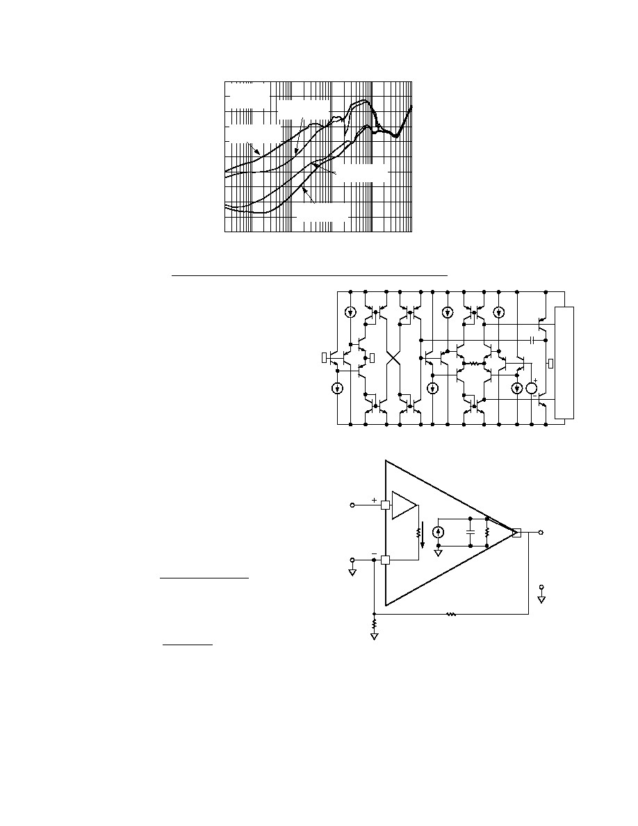
THEORY OF OPERATION
The AD8018 is composed of two current feedback amplifiers
capable of delivering 400 mA of output current while swinging
to within 0.5 V of either power supply, and maintaining low
distortion. A differential line driver using the AD8018 can provide
CPE performance on a single 5 V supply. This performance is
enabled by Analog Device's XFCB process and a novel, two-
stage current feedback architecture featuring a patent-pending
rail-to-rail output stage.
A simplified schematic is shown in Figure 4. Emitter followers
buffer the positive input, V
P
, to provide low input current and
current noise. The low impedance current feedback summing
junction is at the negative input, V
N
. The output stage is another
high-gain amplifier used as an integrator to provide frequency
compensation. The complementary common-emitter output
provides the extended output swing.
A current feedback amplifier's dynamic and distortion performance
is relatively insensitive to its closed-loop signal gain, which is
a distinct advantage over a voltage-feedback architecture. Figure
5 shows a simplified model of a current feedback amplifier. The
feedback signal is a current into the inverting node. R
IN
is inversely
proportional to the transconductance of the amplifier's input stage,
g
mi
. Circuit analysis of the pictured follower with gain yields:
V
V
G
T
T
R
G
R
OUT
IN
Z S
Z S
F
IN
/
( )
( )
= ×
+
+ ×
where:
G
R R
T
R
C
R
R
g
F
G
Z S
T
S
T
T
IN
mi
= +
=
+
=
1
1
1
125
/
(
)
/
( )
Recognizing that G R
IN
< R
F
, and that the 3 dB point is set
when T
Z(S)
= R
F
, one can see that the amplifier's bandwidth
depends primarily on the feedback resistor. There is a value of
R
F
below which the amplifier will be unstable, as an actual ampli-
fier will have additional poles that will contribute excess phase
shift. The optimum value for R
F
depends on the gain and the
amount of peaking tolerable in the application.
FREQUENCY Hz
CROSSTALK
dB
90
1M
10M
100M
1G
80
70
60
50
40
30
20
10
R
L
= 5
SIDE A DRIVEN
R
L
= 5
SIDE B DRIVEN
V
IN
= 2V p-p
G = 2
V
S
= 2.5
100k
R
L
= 100
SIDE A DRIVEN
R
L
= 100
SIDE B DRIVEN
100
110
TPC 25. Crosstalk vs. Frequency
V
O
BIAS
V
N
V
P
Figure 4. Simplified Schematic
G = 1
I
T
= I
IN
C
T
R
T
I
IN
V
OUT
R
G
R
F
R
IN
+
V
IN
V
O
+
Figure 5. Model of Current Feedback Amplifier
FEEDBACK RESISTOR SELECTION
In current feedback amplifiers, selection of the feedback and gain
resistors will impact on the MTPR performance, bandwidth,
noise, and gain flatness. Care should be exercised in the selection
of these resistors so that the optimum performance is achieved.
Table I shows the recommended resistor values for use in a variety
of gain settings for the test circuit in TPC 1. These values are
intended to be a starting point when designing for any application.
REV. 0
AD8018
9
Table I. Resistor Selection Guide
Gain
R
F
( )
R
G
( )
1
681
681
+1
1 k
+2
750
750
+3
511
256
+4
340
113
+5
230
59
POWER-DOWN FEATURES
Two digitally programmable logic pins, PWDN1 and PWDN0,
are available on the TSSOP-14 package to select among three
different modes of operation, full power, standby and shutdown.
The DGND pin is the logic ground reference. The logic thresh-
old voltage is established 1 V above DGND. In a typical 5 V
single-supply application, the DGND pin is connected to analog
ground. If PWDN1, PWDN0, and DGND are left unconnected,
the AD8018 will operate at full power.
Table II. Power-Down Features and Truth Table
Supply
Output
PWDN0
PWDN1
State
Current
Impedance
High
High
Full Power
18 mA
Low
Low
High
Standby
9 mA
Low
High
Low
Standby
9 mA
Low
Low
Low
Disabled
300
µA
High
POWER SUPPLY AND DECOUPLING
The AD8018 can be powered with a good quality (i.e., low-noise)
supply anywhere in the range from 3.3 V to 8 V. However, in
order to optimize the ADSL upstream drive capability to +13 dBm
and maintain the best Spurious Free Dynamic Range (SFDR),
the AD8018 circuit should be supplied with a well regulated 5 V
supply. The 5 V supplied at the USB port may be poorly regu-
lated. Improving the quality of the 5 V supply will optimize the
performance of the AD8018 in a USB-supplied CPE ADSL
modem. This can be accomplished through the use of a step-up
dc-to-dc converter or switching power supply followed by a low
dropout (LDO) regulator such as the ADP3331 (see Figure 6).
Setting R1 to be 953 k
and R2 to be 301 k will result in a
V
OUT
of 5 V.
Careful attention must be paid to decoupling the power supply
pins at the output of the dc-to-dc converter, the output of the
LDO regulator and the supply pins of the AD8018. High-quality
capacitors with low equivalent series resistance (ESR) such as
multilayer ceramic capacitors (MLCCs) should be used to mini-
mize supply voltage ripple and power dissipation. A large, usually
tantalum, 10
µF to 47 µF capacitor located in proximity to the
AD8018 is required to provide good decoupling for lower fre-
quency signals. In addition, 0.1
µF MLCC decoupling capacitors
should be located as close to each of the power supply pins as is
physically possible, no more than 1/8 inch away. An additional
large (4.7
µF to 10 µF) tantalum capacitor should be placed on the
board near the supply terminals to supply current for fast, large-
signal changes at the AD8018 outputs.
ADP3331
C1
0.47 F
V
IN
ON
OFF
V
OUT
E
OUT
C2
0.47 F
R3
330k
IN
SD
GND
OUT
FB
ERR
R1
953k
R2
301k
Figure 6. ADP3331 LDO
METHOD FOR GENERATING A MIDSUPPLY VOLTAGE
To operate an amplifier on a single voltage supply, a voltage
midway between the supply and ground must be generated to
properly bias the inputs and the outputs.
A voltage divider can be created with two equal value resistors
(Figure 7). There is a trade-off between the power consumed by
the divider and the voltage drop across these resistors due to the
positive input bias currents. Selecting 2.5 k
for R1 and R2 will
create a voltage divider that draws only 1 mA from a 5 V supply.
The voltage generated with this topology can vary due to the
temperature coefficient (TC) of resistance. Resistors that are
closely matched and have a low TC will minimize variations in
the voltage reference due to temperature. One should also be
sure to use a decoupling capacitor (0.1
µF) at the node where
V
REF
is generated.
5V
R1
2.5k
R2
2.5k
V
REF
0.1 F
Figure 7. Midsupply Reference
DIFFERENTIAL TESTING
The test circuit shown in TPC 13 is used for measuring the dif-
ferential distortion of the AD8018. A single-ended test signal is
applied to the inverting input of the AD8138 differential driver
with the noninverting input grounded. Applying the differential
output of the AD8138 through 100
resistors serves to isolate
the inputs of the AD8018 differential driver and provide a well-
balanced low-distortion input signal. The differential load (R
L
)
of the AD8018 can be set to the equivalent of the line imped-
ance reflected through a transformer. The AD9632 converts
the differential output voltage back to a single-ended signal.
The differential-to- single-ended converter using the AD9632
has an attenuation of 26 dB and is wired with precision resis-
tors to optimize the balance of differential input signal. The
resulting smaller output signal can be easily measured using a
50
spectrum analyzer.
REV. 0
AD8018
10
P
V rmsV
V rms
R
I V
P
TOT
O
S
O
L
Q
S
OUT
=
×
+
+
4 0 8
1
2
2
( .
)
For the AD8018, operating on a single 5 V supply and deliver-
ing a total of 16 dBm (13 dBm to the line and 3 dBm to the
matching network) into 12.5
(100 reflected back through
a 1:4.0 transformer plus back termination), the power is:
= 261 mW + 40 mW
= 301 mW
Using these calculations, and a
JA
of 115
°C/W for the TSSOP
package and 100
°C/W for the SOIC, Tables III and IV show
junction temperature versus power delivered to the line for sev-
eral supply voltages.
Table III. Junction Temperature vs. Line Power and
Operating Voltage for TSSOP, T
AMB
= 85 C
V
SUPPLY
P
LINE
5
6
7
8
13
115
122
129
136
14
117
125
132
140
15
119
127
136
144
16
121
130
139
148
17
123
133
143
153
18
125
136
147
158
Table IV. Junction Temperature vs. Line Power and
Operating Voltage for SOIC, T
AMB
= 85 C
V
SUPPLY
P
LINE,
dBm
5
6
7
8
13
111
117
123
129
14
113
119
126
133
15
115
122
129
136
16
116
124
132
140
17
118
127
136
144
18
120
130
139
149
Running the AD8018 at voltages near 8 V can produce junction
temperatures that exceed the thermal rating of the TSSOP pack-
ages and should be avoided. The shaded areas indicate junction
temperatures greater than 150
°C.
LAYOUT CONSIDERATIONS
As is the case with all high-speed applications, careful attention
to printed circuit board layout details will prevent associated
board parasitics from becoming problematic. Proper RF design
technique is mandatory. The PCB should have a ground plane
covering all unused portions of the component side of the board
to provide a low-impedance return path. Removing the ground
plane on all layers from the area near the input and output pins
will reduce stray capacitance, particularly in the area of the
inverting inputs. Signal lines connecting the feedback and gain
resistors should be as short as possible to minimize the inductance
and stray capacitance associated with these traces. Termination
resistors and loads should be located as close as possible to their
respective inputs and outputs. Input and output traces should
be kept as far apart as possible to minimize coupling (crosstalk)
though the board. Adherence to stripline design techniques for
long signal traces (greater than about 1 inch) is recommended.
This circuit requires significant power supply bypassing. The
AD8018 operates on a split supply in this circuit. The bypassing
technique shown in TPC 13 utilizes a 220
µF tantalum capacitor
and a 0.1
µF ceramic chip capacitor in parallel, connected from
the positive to negative supply, and a 10
µF tantalum and 0.1 µF
ceramic chip capacitor in parallel, connected from each supply to
ground. The capacitors connected between the power supplies
serve to minimize any voltage ripples that might appear at the
supplies while sourcing or sinking any large differential current.
The large capacitor has a pool of charge instantly available for
the AD8018 to draw from, thus preventing any erroneous dis-
tortion results.
POWER DISSIPATION
It is important to consider the total power dissipation of the
AD8018 in order to properly size the heat sink area of an
application. Figure 8 is a simple representation of a differential
driver. With some simplifying assumptions we can estimate the
total power dissipated in this circuit. If the output current is
large compared to the quiescent current, computing the dissipa-
tion in the output devices and adding it to the quiescent power
dissipation will give a close approximation of the total power
dissipation in the package. A factor
(~0.6-1) corrects for the
slight error due to the Class A/B operation of the output stage.
It can be estimated by subtracting the quiescent current in the
output stage from the total quiescent current and ratioing that
to the total quiescent current. For the AD8018,
= 0.833.
+V
S
V
S
+V
O
+V
S
V
S
V
O
R
L
Figure 8. Simplified Differential Driver
Remembering that each output device dissipates for only half
the time gives a simple integral that computes the power for
each device:
1
2
2
×
(
)
V
V
V
R
S
O
O
L
The total supply power can then be computed as:
P
V
V
V
R
I V
P
TOT
S
O
O
L
Q
S
OUT
=
-
×
+
+
4
1
2
2
|
|
In this differential driver, V
O
is the voltage at the output of one
amplifier, so 2 V
O
is the voltage across R
L,
which is the total
impedance seen by the differential driver, including back ter-
mination. Now, with two observations, the integrals are easily
evaluated. First, the integral of V
O
2
is simply the square of the
rms value of V
O
. Second, the integral of |V
O
| is equal to the
average rectified value of V
O
, sometimes called the Mean Aver-
age Deviation, or MAD. It can be shown that for a DMT signal,
the MAD value is equal to 0.8 times the rms value.

REV. 0
AD8018
11
Following these generic guidelines will improve the performance
of the AD8018 in all applications.
To optimize the AD8018's performance as an ADSL differential
line driver, locate the transformer hybrid near the AD8018 drivers
and as close to the RJ11 jack as possible. Maintain differential
circuit symmetry into the differential driver and from the output
of the drivers through the transformer-coupled output of the bridge
circuit as much as possible.
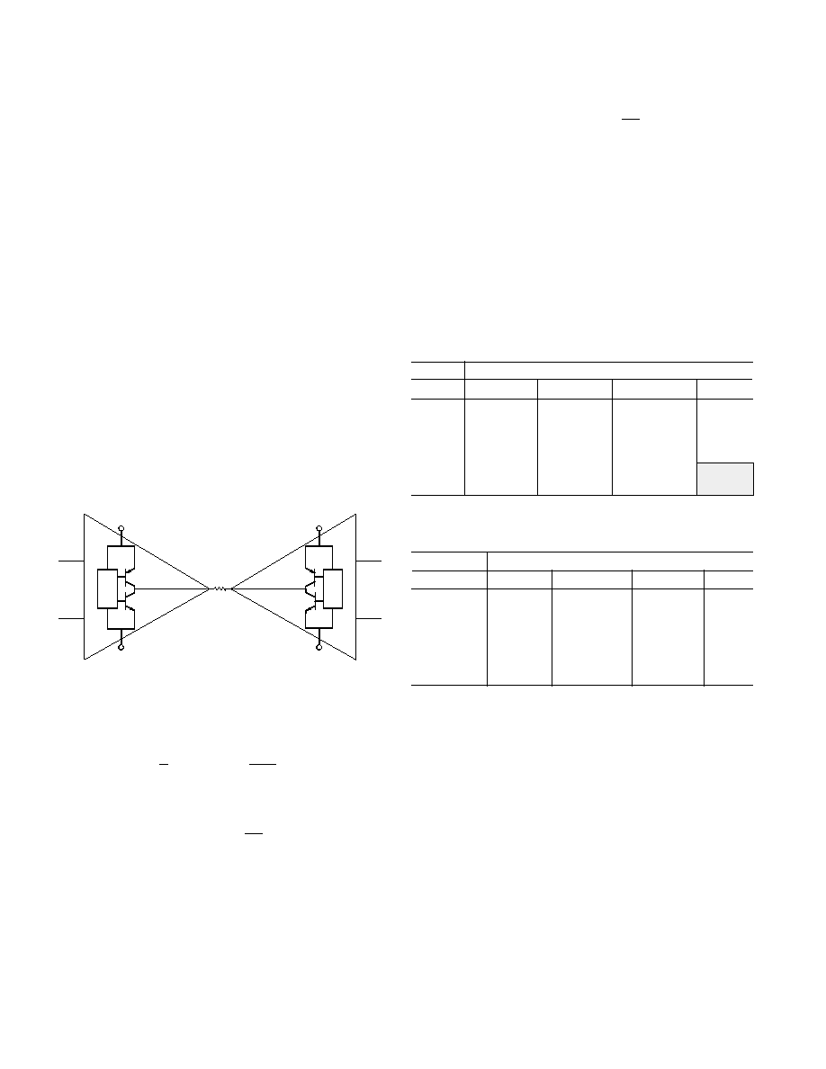
CPE ADSL Application
The low-cost, high-output current dual AD8018 xDSL driver
amplifiers have been specifically designed to drive high fidelity
xDSL signals to within 0.5 V of the power rails, the performance
needed to provide CPE ADSL on a single 5 V supply. The
AD8018 may be used in transformer-coupled bridge hybrid cir-
cuits to drive modulated signals including Discrete MultiTone
(DMT) upstream to the central office.
Evaluation Board
The AD8018ARU-EVAL evaluation board circuit in Figure 12
offers the ability to evaluate the AD8018 in a typical xDSL bridge
hybrid circuit.
The receiver circuit on these boards is typically unpopulated.
Requesting samples of the AD8022AR with the AD8018ARU-
EVAL board will provide the capability to evaluate the
AD8018ARU along with other Analog Devices products in a typi-
cal transceiver circuit. The evaluation circuits have been designed
to replicate the CPE side analog transceiver hybrid circuits.
The circuit mentioned above is designed using a one-transformer
transceiver topology including a line receiver, line driver, line
matching network, an RJ11 jack for interfacing to line simulators,
and transformer-coupled inputs for single-ended-to-differential
input conversion.
AC-coupling capacitors of 0.01
µF, C8, and C10, in combina-
tion with 10 k
resistors R24 and R25, will form a zero frequency
at 1.6 kHz.
Transformer Selection
Customer premise ADSL requires the transmission of a +13 dBm
(20 mW) DMT signal. The DMT signal can have a crest factor
as high as 5.3, requiring the line driver to provide peak line power
of 27.5 dBm (560 mW). 27.5 dBm peak line power translates
into a 7.5 V peak voltage on the 100
telephone line. Assuming
that the maximum low-distortion output swing available from
the AD8018 line driver on a 5 V supply is 4 V and, taking into
account the power lost due to the termination resistance, a step-up
transformer with turns ratio of 4.0 or greater is needed.
In the simplified differential drive circuit shown in Figure 2, the
AD8018 is coupled to the phone line through a step-up trans-
former with a 1:4 turns ratio. R1 and R2 are back-termination
or line-matching resistors, each 3.1
(100 /(2 × 4
2
)), where
100
is the approximate phone line impedance. The total dif-
ferential load for the AD8018, including the termination resistors,
is 12.5
. Even under these conditions the AD8018 provides low
distortion signals to within 0.5 V of the power rails.
Stability Enhancements
The CPE bridge hybrid circuit presents a complex impedance to
the drive amplifiers, particularly when transformer parasitics are
factored in. To ensure stable operation under the full range of
load conditions, a series R-C network (Zoebel Network) should
be connected between each amplifier's output and ground. The
recommended values are 10
for the resistor and 1 nF for the
capacitor to create a low impedance path to ground at frequen-
cies above 16 MHz (see Figure 2). R33 and R34 are added to
improve common-mode stability.
Receive Channel Considerations
A transformer used at the output of the differential line driver to
step up the differential output voltage to the line has the inverse
effect on signals received from the line. A voltage reduction
or attenuation equal to the inverse of the turns ratio is realized
in the receive channel of a typical bridge hybrid. The turns ratio
of the transformer may also be dictated by the ability of the receive
circuitry to resolve low-level signals in the noisy twisted pair tele-
phone plant. Higher turns ratio transformers effectively reduce the
received signal-to-noise ratio due to the reduction in the received
signal strength.
The AD8022, a dual amplifier with typical RTI voltage noise of
only 2.5 nV/
Hz and a low supply current of 4 mA/amplifier, is
recommended for the receive channel.
DMT Modulation, MultiTone Power Ratio (MTPR), and
Out-of-Band SFDR
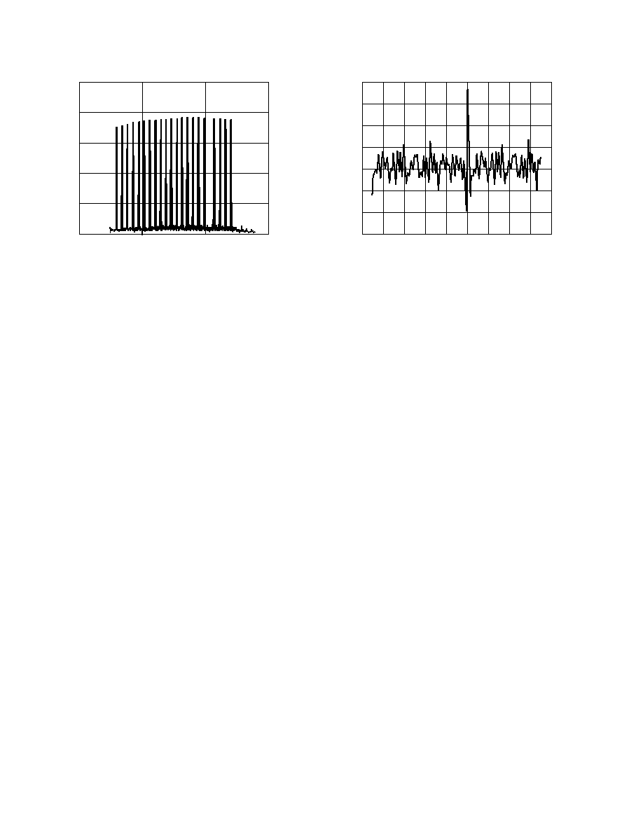
ADSL systems rely on DMT modulation to carry digital data
over phone lines. DMT modulation appears in the frequency
domain as power contained in several individual frequency
subbands, sometimes referred to as tones or bins, each of which
is uniformly separated in frequency. A uniquely encoded, Quadra-
ture Amplitude Modulation (QAM)-like signal occurs at the center
frequency of each subband or tone. See Figure 9 for an example
of a DMT waveform in the frequency domain, and Figure 10 for
a time domain waveform. Difficulties will exist when decoding
these subbands if a QAM signal from one subband is corrupted
by the QAM signal(s) from other subbands, regardless of whether
the corruption comes from an adjacent subband or harmonics of
other subbands.
Conventional methods of expressing the output signal integrity
of line drivers, such as single-tone harmonic distortion or THD,
two-tone InterModulation Distortion (IMD), and third order
intercept (IP3), become significantly less meaningful when
amplifiers are required to process DMT and other heavily
modulated waveforms. A typical ADSL upstream DMT signal
can contain as many as 27 carriers (subbands or tones) of
QAM signals. MultiTone Power Ratio (MTPR) is the relative
difference between the measured power in a typical subband (at
one tone or carrier) versus the power at another subband spe-
cifically selected to contain no QAM data. In other words, a
selected subband (or tone) remains open or void of intentional
power (without a QAM signal), yielding an empty frequency bin.
MTPR, sometimes referred to as the "empty bin test," is
typically expressed in dBc, similar to expressing the relative
difference between single-tone fundamentals and second or
third harmonic distortion components. Measurements of MTPR
are typically made on the line side or secondary side of the
transformer.
REV. 0
AD8018
12
FREQUENCY kHz
20
80
0
150
50
POWER
dBm
100
60
40
20
0
Figure 9. DMT Waveform in the Frequency Domain
MTPR versus transformer turns ratio is depicted in TPC 21 and
covers a variety of line power ranging from +12 dBm to +14 dBm.
As the turns ratio increases, the driver hybrid can deliver more
undistorted power due to higher output current capability.
Significant degradation of MTPR will occur if the output of the
driver swings to the rails, causing clipping at the DMT voltage
peaks. Driving DMT signals to such extremes not only compro-
mises "in-band" MTPR, but will also produce spurs that exist
outside of the frequency spectrum containing the desired DMT
power. "Out-of-band" spurious free dynamic range (SFDR) can
be defined as the relative difference in amplitude between these
spurs and a tone in one of the upstream bins. Compromising
out-of-band SFDR is equivalent to increasing near end cross-
talk (NEXT). Regardless of terminology, maintaining out-of-band
SFDR while reducing NEXT will improve the overall performance
of the modems connected at either end of the twisted pair.
TPC 21 shows how SFDR varies versus transformer turns ratio
for line power ranging from +12 dBm to +14 dBm. As line
power increases, or turns ratio decreases, SFDR degrades. The
power contained in the spurs can be measured relative to the
power contained in a typical upstream carrier and is expressed
in dBc as SFDR, similar to MTPR.
The supply voltage of the driver can also affect SFDR. As the
supply voltage is increased, voltage swing is increased as well,
resulting in the ability to deliver more power to the line with-
out sacrificing performance. This can be seen in TPC 22. Less
undistorted power is available when lower turns ratio transform-
ers are used due to voltage clipping of the signal.
TxDAC is a trademark of Analog Devices, Inc.
TIME ms
4
0.25
VOLTS
0
3
1
0
2
0.2
1.5
1.0
0.05
0.05
1.0
1.5
0.2
3
2
1
Figure 10. DMT Signal in the Time Domain
Generating DMT Signals
At this time, DMT-modulated waveforms are not typically
menu-selectable items contained within AWGs. Even using
AWG software to generate DMT signals, AWGs that are available
today may not deliver DMT signals sufficient in performance
with regard to MTPR due to limitations in the D/A converters
and output drivers used by AWG manufacturers. Similar to
evaluating single-tone distortion performance of an amplifier,
MTPR evaluation requires a DMT signal generator capable of
delivering MTPR performance better than that of the driver
under evaluation. Generating DMT signals can be accom-
plished using a Tektronics AWG 2021 equipped with Option
4, (12-/24-bit, TTL Digital Data Out), digitally coupled to
Analog Devices' AD9754, a 14-bit TxDAC
®
, buffered by an
AD8002 amplifier configured as a differential driver. Note that
the DMT waveforms (available on the Analog Devices website,
http://www.analog.com), or similar .WFM files are needed to
produce the digital data required to drive the TxDAC from the
optional TTL Digital Data output of the TEK AWG2021.
REV. 0
AD8018
13
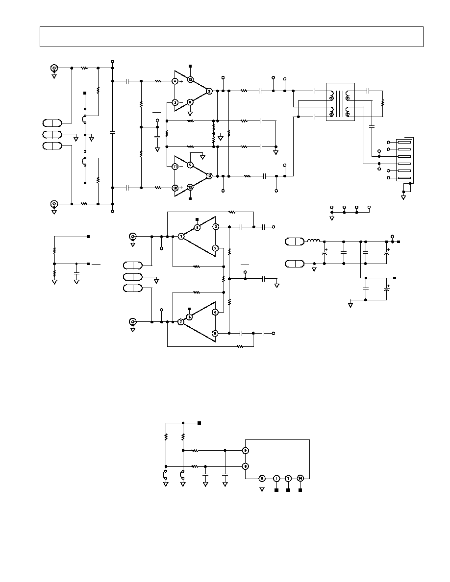
U1
AD8018
+V
R18
750
TP6
R8
100
R3
10
R19
750
R4
10
C22
1000pF
C27
1000pF
U1
AD8018
+V
TP8
R21
DNI
C12
DNI
TP9
PR2
R1
10
1WATT
R2
750
V
CC
-T
U2
AD8022
DNI
R6
DNI
TP17
R7
DNI
VCC-R
AGND;4
V
CC
;8
AGND;4
TP18
R13
DNI
C16
DNI
C3
DNI
TP5
R12
DNI
C1
DNI
C2
DNI
TP4
R9
DNI
R10
DNI
C5
0.1 F
R29
10k
R24
10k
C8
0.1 F
TP10
C10
0.1 F
R14
100
TP11
C28
DNI
R30
0
V
CC
R11
50
R15
50
V
CC
P4
2
P4
1
P4
3
55
53
P3
2
P3
3
P3
1
54
56
R5
DNI
V
CC
R17
2.49k
JP4
A
B
3
2
JP3
1
1
2
3
B
A
C4
DNI
CAPPOLY
C7
DNI
CAPPOLY
NC = 5,6
T1
3
2
1
4
8
9
7
10
1
2
3
4
5
6
TP1
7
8
TP2
C9
DNI
CAPPOLY
CAPPOLY
C6
DNI
TB1 1
C18
DNI
V
CC
-T
TP19
C17
10 F
25V
C15
0.01 F
C26
0.1 F
C14
10 F
L5
BEAD
2
TB1
C19
DNI
25V
C23
DNI
U2 DECOUPLING
TP23 TP24 TP25 TP26
R32
DNI
1
2
R20
DNI
C11
DNI
TP7 PR1
R31
0
V
CC
-R
V
CC
-R
DNI: DO NOT INSTALL
V
CC
2
V
CC
2
V
CC
-T
R33
10k
R34
10k
R16
2.49k
C20
0.1 F
U2
AD8022
DNI
V
CC
2
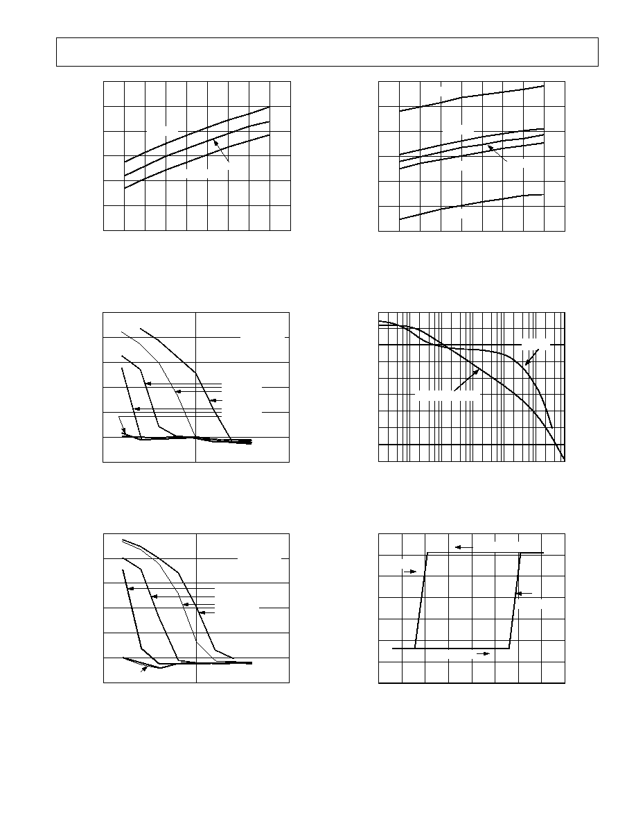
Figure 11. EVAL Board Schematic
JP1
NC1 NC2 NC3
PDN0
PDN1
DGND
U1
AD8018
0.1 F
C25
0.1 F
C24
100
R25
100
R26
R28
DNI
R27
DNI
V
CC
JP2
Figure 12. Input Control Circuit
REV. 0
AD8018
14
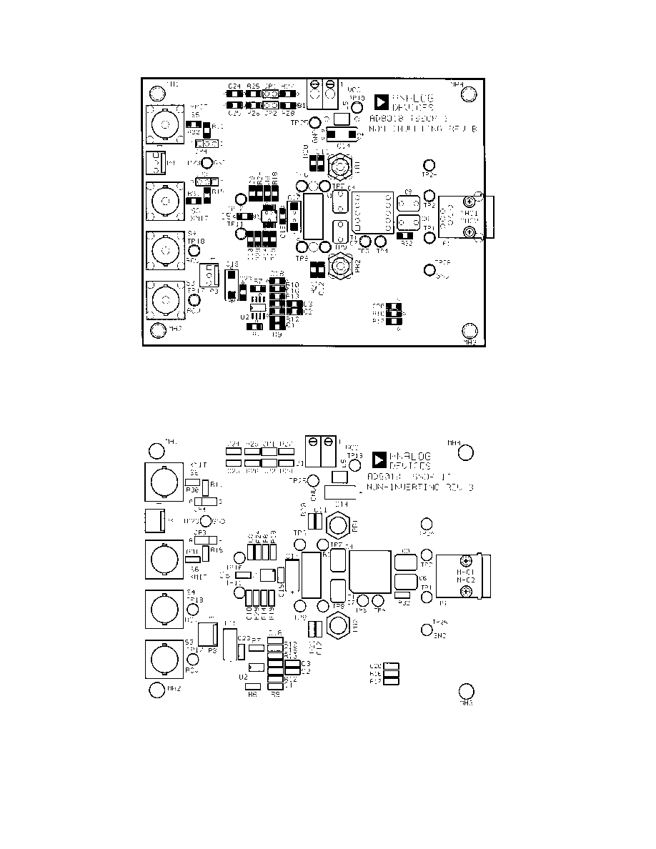
Figure 13. Assembly--Primary Side
Figure 14. Silk Screen--Primary Side
REV. 0
AD8018
15
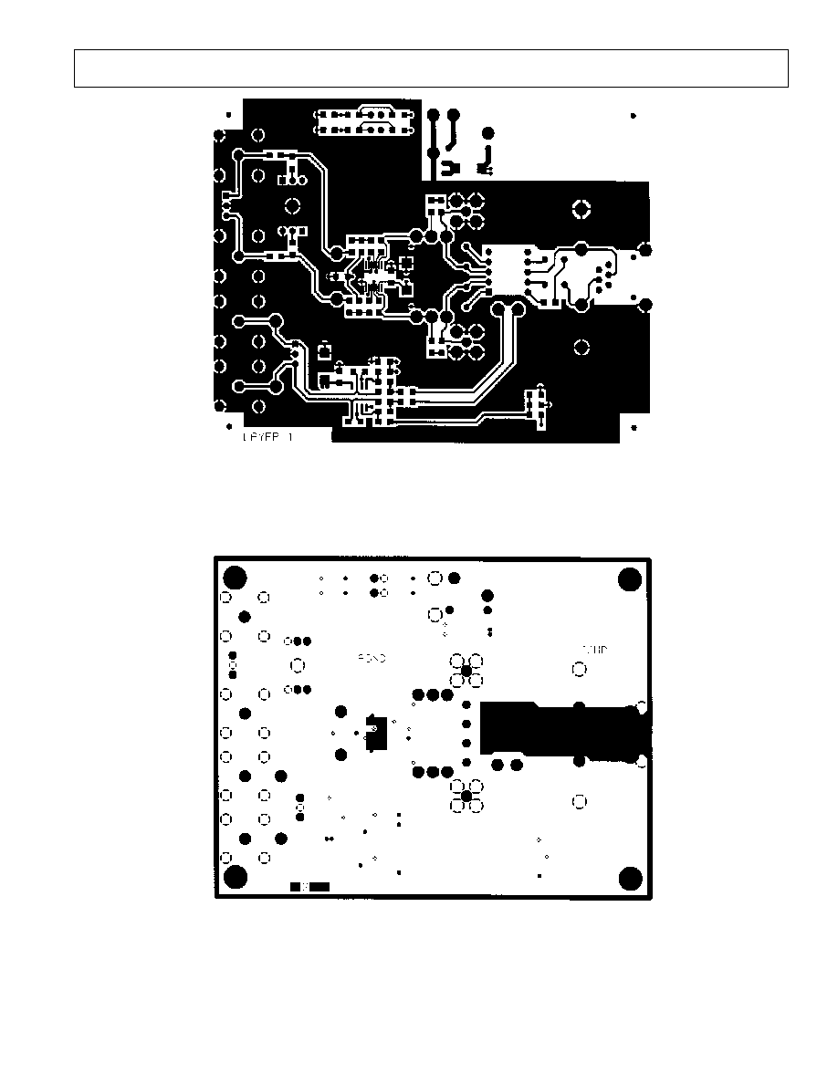
Figure 15. Layer 1--Primary Side
Figure 16. Layer 2--Ground Plane
REV. 0
AD8018
16
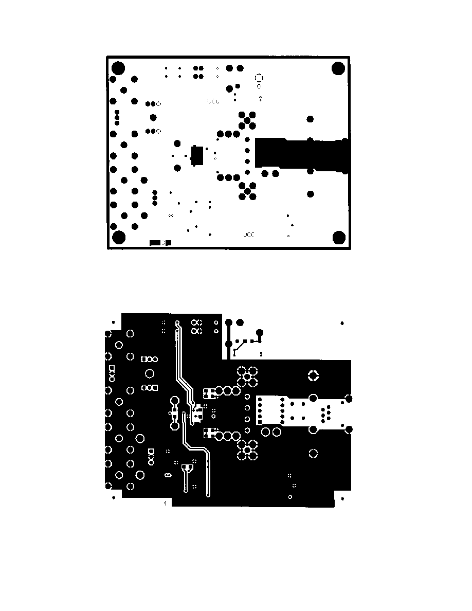
Figure 17. Layer 3--Power Plane
Figure 18. Layer 4--Secondary Side
REV. 0
AD8018
17
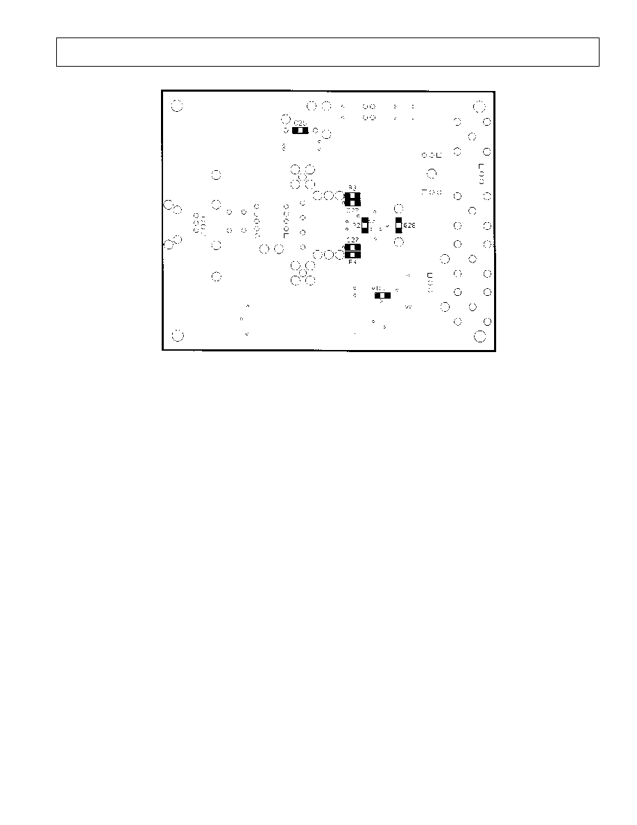
Figure 19. Assembly--Secondary Side

REV. 0
AD8018
18
EVALUATION BOARD--BILL OF MATERIALS
Qty.
Description
Vendor
Ref Desc.
2
1,000 pF 50 V. 1206 ceramic chip capacitor
ADS # 4-5-20
C22, 27
2
0.01
µF 50 V. 1206 ceramic chip capacitor
ADS # 4-5-19
C15, 23
5
0.1
µF 50 V. 1206 size ceramic chip capacitor
ADS # 4-5-18
C5, 20, 24 -26
2
1.0
µF 16 V. 1206 size ceramic chip capacitor
Newark # 83F6841
C8, 10
4
# 26 red (solid) wire jumper
ADS # 10-14-3
C4, 6, 7, 9
3
10
µF 16 V. `C' size Tantalum chip capacitor
ADS # 4-7-6
C14, 17, 19
1
Ferrite bead (with # 22 wire)
ADS # 48-1-1
L5
1
10
5% 3.0 W. metal oxide power resistor
D-K # P10W-3BK-ND
R1
6
0
5% 1/8 W. 1206 size chip resistor
ADS # 3-18-88
C11, 12, R20, 21, 30, 31
2
10.0
1% 1/8 W. 1206 size chip resistor
ADS # 3-18-120
R3, 4
2
49.9
1% 1/8 W. 1206 size chip resistor
ADS # 3-14-26
R11, 15
5
100
1% 1/8 W. 1206 size chip resistor
ADS # 3-18-40
R 8, 14, 25, 26, 32
2
2.49 k
1% 1/8 W. 1206 size chip resistor
ADS # 3-18-71
R16, 17
3
750
1% 1/8 W. 1206 size chip resistor
ADS # 3-18-8
R2, 18, 19
2
10.0 k
0.1% 0805 size chip resistor
ADS # 3-36-5
R33, 34
2
10.0 k
1% 1/8 W. 1206 size chip resistor
ADS # 3-18-119
R24 and 29
4
Test Point (Black) [GND]
ADS # 12-18-44
TP2326 (GND.)
2
Test Point (Brown)
ADS # 12-18-59
TP4, 5
3
Test Point (Red)
ADS # 12-18-43
TP1719
4
Test Point (Orange)
ADS # 12-18-60
TP1, 2, 10, 11
1
Test Point (Yellow)
ADS # 12-18-32
TP3
2
Test Point (Blue)
ADS # 12-18-62
TP6, 8
2
Test Point (Green)
ADS # 12-18-61
TP7, 9
1
2
× 5-pin strips (1/4 of a 20-pin Samtek `SIP' strip socket)
ADS # 11-2-14
(T1)
1
2 Pos. GRAY term. blk. # 25.161.0253 (Newark # 51F4106)
ADS# 12-19-10
TB1, 2
4
0.1 inch ctr. shunt Berg # 65474 -001
ADS # 11-2-38
JP14
2
2 pin gold male header 0.1 inch ctr. Berg # 69157 -102
ADS # 11-2-37
JP1, 2
4
50
BNC pc mount Telegartner # J01001A1944
ADS # 12-6-22
S36
1
AMP# 555154 -1 MOD. JACK (SHIELDED) 6 6
ADS # 12-20-5
P1
2
3-pin gold male header Waldom D-K # WM 2723 -ND
ADS # 12-3-80
JP3, 4
2
3-pin gold male locking header Waldom # WM 2701 -ND
ADS # 12-3-79
P3, 4
1
AD8018ARU ADSL Driver hybrid
ADS # AD8018ARU
U1 (D.U.T.)
1
AD8018 TSSOP1T Non-Inverting REV. A Evaluation PC board
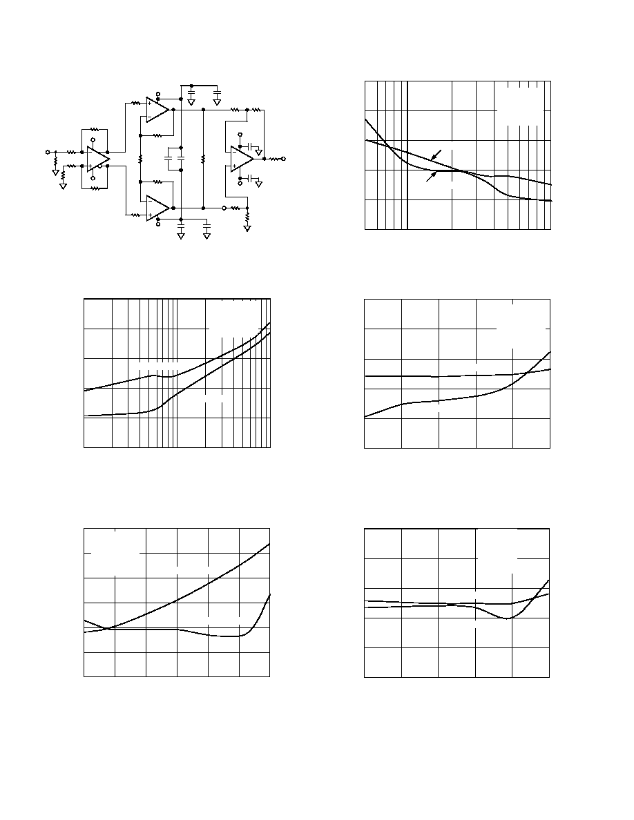
D C S
Eval. PC Board
4
# 4 40
× 1/4" panhead ss machine screw
ADS # 30-1-1
4
# 4 40
× 1/2" threaded alum. standoffs
ADS # 30-16-2
REV. 0
AD8018
19
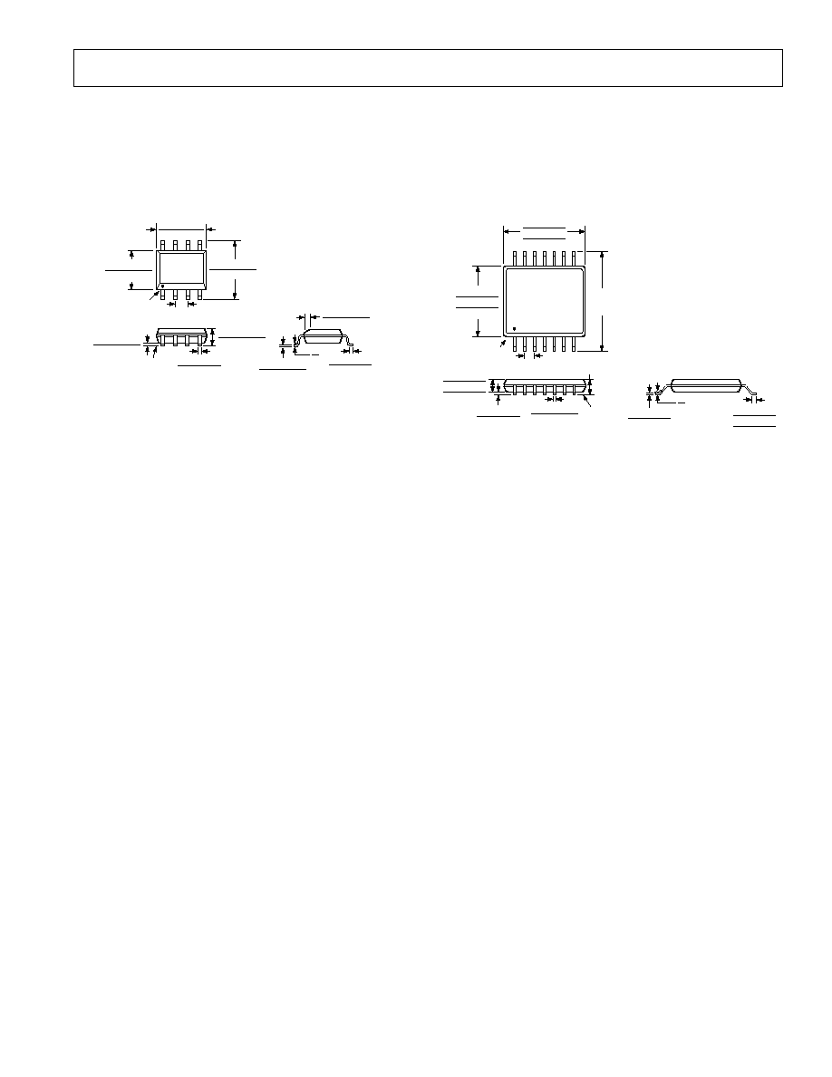
OUTLINE DIMENSIONS
Dimensions shown in inches and (mm).
8 Lead SOIC
(SO-8)
0.0098 (0.25)
0.0075 (0.19)
0.050 (1.27)
0.016 (0.40)
8
0
0.0196 (0.50)
0.0099 (0.25)
45
8
5
1
0.1968 (5.00)
0.1890 (4.80)
0.2440 (6.20)
0.2284 (5.80)
PIN 1
0.1574 (4.00)
0.1497 (3.80)
0.0500 (1.27)
BSC
0.0688 (1.75)
0.0532 (1.35)
SEATING
PLANE
0.0098 (0.25)
0.0040 (0.10)
0.020 (0.51)
0.013 (0.33)
CONTROLLING DIMENSIONS ARE IN MILLIMETERS
ALL DIMENSIONS PER JEDEC STANDARDS MS-012 AA
14 Lead TSSOP
(RU-14)
0.177 (4.50)
0.173 (4.40)
0.169 (4.30)
14
8
7
1
0.252
(6.40)
BSC
PIN 1
0.201 (5.10)
0.197 (5.00)
0.193 (4.90)
0.0256 (0.65)
BSC
SEATING
PLANE
0.006 (0.15)
0.002 (0.05)
0.0118 (0.30)
0.0075 (0.19)
0.047 (1.2)
MAX
0.059 (1.50)
0.093 (1.00)
0.031 (0.80)
0.008 (0.20)
0.004 (0.09)
8
0
0.030 (0.75)
0.024 (0.60)
0.018 (0.45)
CONTROLLING DIMENSIONS ARE IN MILLIMETERS
C015194.57/00 (rev. 0)
PRINTED IN U.S.A.