 | ÐлекÑÑоннÑй компоненÑ: AD8019 | СкаÑаÑÑ:  PDF PDF  ZIP ZIP |
Äîêóìåíòàöèÿ è îïèñàíèÿ www.docs.chipfind.ru
REV. 0
Information furnished by Analog Devices is believed to be accurate and
reliable. However, no responsibility is assumed by Analog Devices for its
use, nor for any infringements of patents or other rights of third parties that
may result from its use. No license is granted by implication or otherwise
under any patent or patent rights of Analog Devices.
a
AD8019
One Technology Way, P.O. Box 9106, Norwood, MA 02062-9106, U.S.A.
Tel: 781/329-4700
www.analog.com
Fax: 781/326-8703
© Analog Devices, Inc., 2001
DSL Line Driver
with Power-Down
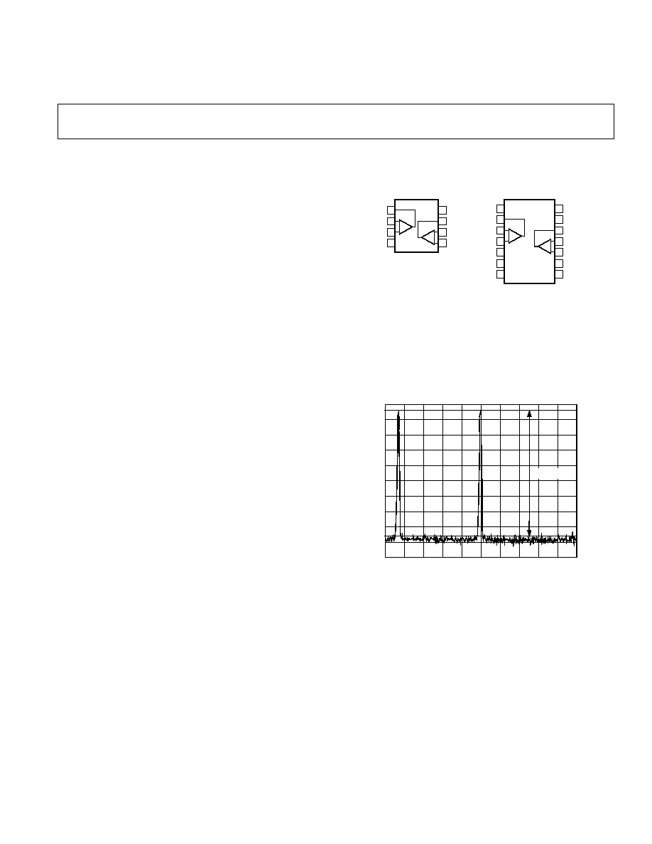
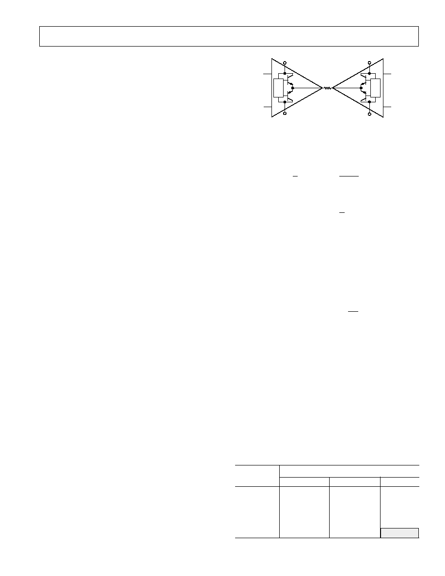
PIN CONFIGURATIONS
8
7
6
5
1
2
3
4
AD8019AR
IN1
OUT1
OUT2
+IN1
V
S
+V
S
IN2
+IN2
14
13
12
11
10
9
8
1
2
3
4
5
6
7
AD8019ARU
NC = NO CONNECT
DGND
NC
PWDN
NC
NC
NC
OUT1
IN1
+IN1
V
S
OUT2
+V
S
IN2
+IN2
FEATURES
Low Distortion, High Output Current Amplifiers
Operate from 12 V to 12 V Power Supplies,
Ideal for High-Performance ADSL CPE, and xDSL
Modems
Low Power Operation
9 mA/Amp (Typ) Supply Current
Digital (1-Bit) Power-Down
Voltage Feedback Amplifiers
Low Distortion
Out-of-Band SFDR 80 dBc @ 100 kHz into 100
Line
High Speed
175 MHz Bandwidth (3 dB), G = +1
400 V/ s Slew Rate
High Dynamic Range
V
OUT
to within 1.2 V of Power Supply
APPLICATIONS
ADSL, VDSL, HDSL, and Proprietary xDSL USB, PCI,
PCMCIA Modems, and Customer Premise Equipment
(CPE)
PRODUCT DESCRIPTION
The AD8019 is a low cost xDSL line driver optimized to drive a
minimum of 13 dBm into a 100
load while delivering outstand-
ing distortion performance. The AD8019 is designed on a 24 V
high-speed bipolar process enabling the use of
± 12 V power
supplies or 12 V only. When operating from a single 12 V sup-
ply the highly efficient amplifier architecture can typically deliver
170 mA output current into low impedance loads through a
1:2 turns ratio transformer. Hybrid designs using
±12 V supplies
enable the use of a 1:1 turns ratio transformer, minimizing attenu-
ation of the receive signal. The AD8019 typically draws 9 mA/
amplifier quiescent current. A 1-bit digital power down feature
reduces the quiescent current to approximately 1.6 mA/amplifier.
Figure 1 shows typical Out of Band SFDR performance under
ADSL CPE (upstream) conditions. SFDR is measured while
driving a 13 dBm ADSL DMT signal into a 100
line with
50
back termination.
The AD8019 comes in thermally enhanced 8-lead SOIC and
14-lead TSSOP packages. The 8-lead SOIC is pin-compatible
with the AD8017 12 V line driver.
FREQUENCY kHz
132.5
10dB/DIV
137.5
142.5
80dBc
Figure 1. Out-of-Band SFDR; V
S
=
±12 V; 13 dBm Output
Power into 200
, Upstream
8-Lead SOIC
(R-8)
14-Lead TSSOP
(RU-14)

REV. 0
2
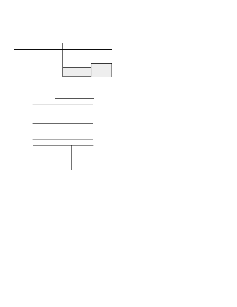
AD8019SPECIFICATIONS
Parameter
Conditions
Min
Typ
Max
Unit
DYNAMIC PERFORMANCE
3 dB Bandwidth
G = +5
35
MHz
G = +1, V
OUT
< 0.4 V p-p, R
L
= 100
175
180
MHz
G = +2, V
OUT
< 0.4 V p-p, R
L
= 100
70
75
MHz
0.1 dB Bandwidth
V
OUT
< 0.4 V p-p, R
L
= 100
6
MHz
G = +5, V
OUT
< 0.4 V p-p, R
L
= 100
35
MHz
Large Signal Bandwidth
V
OUT
= 4 V p-p
50
MHz
Slew Rate
Noninverting, V
OUT
= 4 V p-p
450
V/
µs
Rise and Fall Time
Noninverting, V
OUT
= 2 V p-p
5.5
ns
Settling Time
0.1%, V
OUT
= 2 V p-p
40
ns
NOISE/DISTORTION PERFORMANCE
Distortion
V
OUT
= 3 V p-p (Differential)
Second Harmonic
100 kHz, R
L(DM)
= 50
78
dBc
500 kHz, R
L(DM)
= 50
74
dBc
Third Harmonic
100 kHz, R
L(DM)
= 50
85
dBc
500 kHz, R
L(DM)
= 50
80
dBc
Out-of-Band SFDR
144 kHz1.1 MHz, Differential R
L
= 70
80
dBc
MTPR
25 kHz138 kHz, Differential R
L
= 70
72
dBc
Input Voltage Noise
f = 100 kHz
8
nV/
Hz
Input Current Noise
f = 100 kHz
0.9
pA
Hz
Crosstalk
f = 1 MHz, G = +2
80
dB
DC PERFORMANCE
Input Offset Voltage
8
20
mV
T
MIN
T
MAX
10
23
mV
Input Offset Voltage Match
1
12
mV
T
MIN
T
MAX
2
17
mV
Open-Loop Gain
V
OUT
= 6 V p-p, R
L
= 25
72
80
dB
T
MIN
T
MAX
72
80
dB
INPUT CHARACTERISTICS
Input Resistance
10
M
Input Capacitance
0.5
pF
+Input Bias Current
3
+1
+3
µA
T
MIN
T
MAX
4
+4
µA
Input Bias Current
1.5
0.5
+1.5
µA
T
MIN
T
MAX
1.8
+1.8
µA
+Input Bias Current Match
1.0
0.2
+1.0
µA
T
MIN
T
MAX
1.5
+1.5
µA
Input Bias Current Match
0.5
+0.1
+0.5
µA
T
MIN
T
MAX
0.8
+0.8
µA
CMRR
V
CM
= 4 V to +4 V
71
74
dB
Input CM Voltage Range
2
10
V
OUTPUT CHARACTERISTICS
Output Resistance
0.2
Output Voltage Swing
R
L
= 25
4.8
+4.8
V
Output Current
SFDR 80 dBc into 25
at 100 kHz
175
200
mA
Short Circuit Current
1
400
mA
POWER SUPPLY
Supply Current/Amp
PWDN = 5 V
9
10.5
mA
T
MIN
T
MAX
14.5
mA
PWDN = 0 V
0.8
2.0
mA
Operating Range
Dual Supply
±4.0
±6.0
V
Power Supply Rejection Ratio
±V
S
= +1.0 V to 1.0 V
65
68
dB
LOGIC LEVELS
V
PWDN
= 0 V to 3 V; V
IN
= 10 MHz, G = +5
t
ON
120
ns
t
OFF
80
ns
PWDN = "1" Voltage
1.8
+V
S
V
PWDN = "0" Voltage
0.5
V
PWDN = "1" Bias Current
220
µA
PWDN = "0" Bias Current
100
µA
NOTES
1
This device is protected from overheating during a short-circuit by a thermal shutdown circuit.
Specifications subject to change without notice.
(@ 25 C, V
S
= 12 V, R
L
= 25
, R
F
= 500
, T
MIN
= 40 C, T
MAX
= +85 C, unless
otherwise noted.)

REV. 0
3
AD8019
Parameter
Conditions
Min
Typ
Max
Unit
DYNAMIC PERFORMANCE
3 dB Bandwidth
G = +5
35
MHz
G = +1, V
OUT
< 0.4 V p-p
175
180
MHz
G = +2, V
OUT
< 0.4 V p-p
70
75
MHz
0.1 dB Bandwidth
V
OUT
< 0.4 V p-p
5.5
MHz
Large Signal Bandwidth
V
OUT
= 4 V p-p
50
MHz
Slew Rate
Noninverting, V
OUT
= 4 V p-p
400
V/
µs
Rise and Fall Time
Noninverting, V
OUT
= 2 V p-p
5.5
ns
Settling Time
0.1%, V
OUT
= 2 V p-p
40
ns
NOISE/DISTORTION PERFORMANCE
Distortion
V
OUT
= 16 V p-p (Differential)
Second Harmonic
100 kHz, R
L(DM)
= 200
80
dBc
500 kHz, R
L(DM)
= 200
72
dBc
Third Harmonic
100 kHz, R
L(DM)
= 200
85
dBc
500 kHz, R
L(DM)
= 200
80
dBc
Out-of-Band SFDR
144 kHz500 kHz, Differential R
L
= 200
80
dBc
MTPR
25 kHz138 kHz, Differential R
L
= 200
73
dBc
Input Voltage Noise
f = 100 kHz
8
nV/
Hz
Input Current Noise
f = 100 kHz
0.9
pA
Hz
Crosstalk
f = 1 MHz, G = +2
85
dB
DC PERFORMANCE
Input Offset Voltage
5
20
mV
T
MIN
T
MAX
10
mV
Input Offset Voltage Match
1
12
mV
T
MIN
T
MAX
2
18
mV
Open-Loop Gain
V
OUT
= 18 V p-p, R
L
= 100
86
92
dB
T
MIN
T
MAX
90
dB
INPUT CHARACTERISTICS
Input Resistance
10
M
Input Capacitance
0.5
pF
+Input Bias Current
3
0.5
+3
µA
T
MIN
T
MAX
3.8
+3.8
µA
Input Bias Current
1.5
0.2
+1.5
µA
T
MIN
T
MAX
1.7
+1.7
µA
+Input Bias Current Match
1.0
+0.2
+1.0
µA
T
MIN
T
MAX
2.4
+2.4
µA
Input Bias Current Match
1.0
+0.1
+1.0
µA
T
MIN
T
MAX
2.5
+2.5
µA
CMRR
V
CM
= 10 V to +10 V
71
76
dB
Input CM Voltage Range
10
+10
V
OUTPUT CHARACTERISTICS
Output Resistance
0.2
Output Voltage Swing
R
L
= 100
10.8
+10.8
V
Output Current
SFDR 80 dBc into 100
at 100 kHz
125
170
mA
Short Circuit Current
1
800
mA
POWER SUPPLY
Supply Current/Amp
PWDN = High
9
10
mA
T
MIN
T
MAX
11.5
mA
PWDN = Low
0.8
1.75
mA
Operating Range
Dual Supply
±4.0
±12
V
Power Supply Rejection Ratio
±V
S
= +1.0 V to 1.0 V
61
64
dB
LOGIC LEVELS
V
PWDN
= 0 V to 3 V; V
IN
= 10 MHz, G = +5
t
ON
120
ns
t
OFF
80
ns
PWDN = "1" Voltage
1.8
+V
S
V
PWDN = "0" Voltage
0.5
V
PWDN = "1" Bias Current
220
µA
PWDN = "0" Bias Current
100
µA
NOTES
1
This device is protected from overheating during a short-circuit by a thermal shutdown circuit.
Specifications subject to change without notice.
(@ 25 C, V
S
= 12 V, R
L
= 100
, R
F
= 500
, T
MIN
= 40 C, T
MAX
= +85 C, unless otherwise noted.)
REV. 0
AD8019
4
CAUTION
ESD (electrostatic discharge) sensitive device. Electrostatic charges as high as 4000 V readily
accumulate on the human body and test equipment and can discharge without detection. Although
the AD8019 features proprietary ESD protection circuitry, permanent damage may occur on
devices subjected to high-energy electrostatic discharges. Therefore, proper ESD precautions are
recommended to avoid performance degradation or loss of functionality.
WARNING!
ESD SENSITIVE DEVICE
ABSOLUTE MAXIMUM RATINGS
1
Supply Voltage . . . . . . . . . . . . . . . . . . . . . . . . . . . . . . . . 26.4 V
Internal Power Dissipation
TSSOP-14 Package
2
. . . . . . . . . . . . . . . . . . . . . . . . . 2.2 W
SOIC-8 Package
3
. . . . . . . . . . . . . . . . . . . . . . . . . . . 1.4 W
Input Voltage (Common-Mode) . . . . . . . . . . . . . . . . . . . .
±V
S
Differential Input Voltage . . . . . . . . . . . . . . . . . . . . . . . . .
±V
S
Output Short Circuit Duration
. . . . . . . . . . . . . . . . . . . . Observe Power Derating Curves
Storage Temperature Range . . . . . . . . . . . . 65
°C to +125°C
Operating Temperature Range . . . . . . . . . . . 40
°C to +85°C
Lead Temperature Range (Soldering 10 sec) . . . . . . . . . 300
°C
NOTES
1
Stresses above those listed under Absolute Maximum Ratings may cause perma-
nent damage to the device. This is a stress rating only; functional operation of the
device at these or any other conditions above those indicated in the operational
section of this specification is not implied. Exposure to absolute maximum rating
conditions for extended periods may affect device reliability.
2
Specification is for device on a four-layer board with 10 inches
2
of 1 oz. copper at
85
°C 14-lead TSSOP package:
JA
= 90
°C/W.
3
Specification is for device on a four-layer board with 10 inches
2
of 1 oz. copper at
85
°C 8-lead SOIC package:
JA
= 100
°C/W.
MAXIMUM POWER DISSIPATION
The maximum power that can be safely dissipated by the AD8019
is limited by the associated rise in junction temperature. The
maximum safe junction temperature for a plastic encapsulated
device is determined by the glass transition temperature of the
plastic, approximately 150
°C. Temporarily exceeding this limit
may cause a shift in parametric performance due to a change in
the stresses exerted on the die by the package.
The output stage of the AD8019 is designed for maximum load
current capability. As a result, shorting the output to common
can cause the AD8019 to source or sink 500 mA. To ensure
proper operation, it is necessary to observe the maximum power
derating curves. Direct connection of the output to either power
supply rail can destroy the device.
AMBIENT TEMPERATURE C
MAXIMUM POWER DISSIPATION
W
2.5
2.0
1.5
1.0
0.5
0
40 30 20 10
0
10
20
30
40
50
60
70
80
SOIC
TSSOP
Figure 2. Plot of Maximum Power Dissipation vs.
Temperature for AD8019 for T
J
= 150
°C
ORDERING GUIDE
Temperature
Package
Package
Model
Range
Description
Option
AD8019ARU
40
°C to +85°C
14-Lead TSSOP
RU-14
AD8019ARU-Reel
40
°C to +85°C
14-Lead TSSOP
RU-14 Reel
AD8019ARU-EVAL
40
°C to +85°C
Evaluation Board
ARU-EVAL
AD8019AR
40
°C to +85°C
8-Lead SOIC
R-8
AD8019AR-Reel
40
°C to +85°C
8-Lead SOIC
R-8 Reel
AD8019AR-EVAL
40
°C to +85°C
Evaluation Board
AR EVAL
REV. 0
5
Typical Performance CharacteristicsAD8019
0.1 F
0.1 F
10 F
10 F
49.9
124
499
R
L
V
OUT
+V
S
V
S
+
+
V
IN
TPC 1. Single-Ended Test Circuit; G = +5
TIME ns
V
OUT
mV
100
60
80
100
100
0
100
200
300
400
500
600
700
40
20
0
20
40
60
80
TPC 2. 100 mV Step Response; G = +5, V
S
=
±6 V,
R
L
= 25
, Single-Ended
TIME ns
V
OUT
Volts
3
4
100
0
100
200
300
400
500
600
700
2
1
0
1
2
3
4
TPC 3. 4 V Step Response; G = +5, V
S
=
±6 V,
R
L
= 25
, Single-Ended
500
50
+V
IN
R
L
500
50
V
IN
+V
O
V
O
0.1 F
55
55
0.1 F
0.1 F
V
S
+V
S
+
47 F
TPC 4. Differential Test Circuit; G = +10
TIME 100ns/DIV
VOLTS
mV
80
100
100
0
100
200
300
400
500
600
700
60
40
20
0
20
40
60
80
100
TPC 5. 100 mV Step Response; G = +5, V
S
=
±12 V,
R
L
= 100
, Single-Ended
TIME ns
V
OUT
Volts
3
4
100
0
100
200
300
400
500
600
700
2
1
0
1
2
3
4
TPC 6. 4 V Step Response; G = +5, V
S
=
±12 V,
R
L
= 100
, Single-Ended
REV. 0
AD8019
6
5
FREQUENCY MHz
100
0.01
DISTORTION
dBc
1
0.1
90
80
70
60
50
40
30
20
3RD
2ND
TPC 7. Distortion vs. Frequency; V
S
=
±12 V, R
L
= 200
,
Differential, V
O
= 16 V p-p
100
DISTORTION
dBc
90
80
70
60
50
40
30
PEAK OUTPUT CURRENT mA
50
75
100
125
150
175
200
2ND HARMONIC
3RD HARMONIC
TPC 8. Distortion vs. Peak Output Current; V
S
=
±6 V;
R
L
= 10
; f = 100 kHz; Single-Ended; Second Harmonic
100
DISTORTION
dBc
90
80
70
60
50
40
30
PEAK OUTPUT CURRENT mA
50
75
100
125
150
175
200
225
250
20
2ND HARMONIC
3RD HARMONIC
TPC 9. Distortion vs. Peak Output Current; V
S
=
±12 V;
R
L
= 25
; f = 100 kHz; Single-Ended; Second Harmonic
5
FREQUENCY MHz
100
0.01
DISTORTION
dBc
1
0.1
90
80
70
60
50
40
30
20
3RD
2ND
TPC 10. Distortion vs. Frequency; V
S
=
±6 V, R
L
= 50
,
Differential, V
O
= 3 V p-p
100
DISTORTION
dBc
90
80
70
60
50
40
30
DIFFERENTIAL OUTPUT VOLTAGE V p-p
0
2
4
6
8
10
20
12
14
16
18
20
2ND
3RD
TPC 11. Distortion vs. Output Voltage; f = 100 kHz,
V
S
=
±6 V, G = +10, R
L
= 50
, Differential
100
DISTORTION
dBc
90
80
70
60
50
40
30
DIFFERENTIAL OUTPUT VOLTAGE V p-p
0
2
4
6
8
10
20
12
14
16
18
20
110
10
2ND
3RD
TPC 12. Distortion vs. Output Voltage; f = 500 kHz,
V
S
=
±6 V, G = +10, R
L
= 50
, Differential
REV. 0
AD8019
7
100
DISTORTION
dBc
90
80
70
60
50
40
30
DIFFERENTIAL OUTPUT VOLTAGE V p-p
0
5
10
15
20
25
20
30
35
40
45
50
2ND
3RD
TPC 13. Distortion vs. Output Voltage; f = 100 kHz,
V
S
=
±12 V, G = +10, R
L
= 200
, Differential
100
DISTORTION
dBc
90
80
70
60
50
40
30
DIFFERENTIAL OUTPUT VOLTAGE V p-p
0
5
10
15
20
25
20
30
35
40
45
50
110
10
2ND
3RD
TPC 14. Distortion vs. Output Voltage; f = 500 kHz,
V
S
=
±12 V, G = +10, R
L
= 200
, Differential
10
0.5
100
1
0.1
0.6
0.8
0.9
1.0
1.1
1.2
LOAD CURRENT mA
OUTPUT SATURATION VOLTAGE
Volts
0.7
1000
40 C
+25 C
+85 C
V
OL
V
OH
V
OH
V
OH
V
OL
V
OL
TPC 15. Output Saturation Voltage vs. Load; V
S
=
±12 V,
V
S
=
±6 V
1000
FREQUENCY MHz
19
1
OUTPUT VOLTAGE
dBV
100
10
16
13
10
7
4
1
2
5
8
11
TPC 16. Output Voltage vs. Frequency; V
S
=
±12 V,
R
L
= 100
; G = +5
1000
FREQUENCY MHz
90
1
CMRR
dB
100
10
80
70
60
50
40
30
0
0.1
0.01
20
10
V
IN
909
909
909
909
50
50
50
V
OUT
TPC 17. CMRR vs. Frequency; V
S
=
±12 V, R
L
= 100
1000
FREQUENCY MHz
19
1
OUTPUT VOLTAGE
dBV
100
10
16
13
10
7
4
1
2
5
8
11
TPC 18. Output Voltage vs. Frequency; V
S
=
±6 V,
R
L
= 100
; G = +5
REV. 0
AD8019
8
1000
FREQUENCY MHz
90
1
PSRR
dB
100
10
80
70
60
50
40
30
0.1
0.01
20
10
PSRR
+PSRR
TPC 19. PSRR vs. Frequency; R
L
= 100
1000
FREQUENCY kHz
1
100
10
0.1
0.01
I
NOISE
V
NOISE
+I
NOISE
V
NOISE
nV Hz
1
10
100
0.1
100
10
1
0.1
I
NOISE
pA Hz
TPC 20. Noise vs. Frequency
20ns/DIV
2mV/DIV
0.1%
V
IN
V
OUT
1.1k
1.1k
V
IN
V
OUT
50
50
50
6.8pF
TPC 21. Settling Time 0.1%; V
S
=
±12 V, R
L
= 100
,
V
OUT
= 2 V p-p
1000
FREQUENCY MHz
90
1
CROSSTALK
dB
100
10
80
70
60
50
40
30
0.1
0.01
20
100
TPC 22. Crosstalk vs. Frequency, V
S
=
±12 V, V
S
=
±6 V;
G = +2; V
IN
= 10 dBm
FREQUENCY MHz
20
0.001
GAIN
dB
0
0.01
1000
0.1
1
10
100
10
10
20
30
40
50
60
70
80
90
100
110
120
2k
50
10
500
10
50
50
50
50
A
OL
PHASE
45
PHASE
Degrees
0
45
90
135
180
225
270
TPC 23. Open-Loop Gain and Phase vs. Frequency
V
IN
20ns/DIV
2mV/DIV
0.1%
1.1k
1.1k
V
IN
V
OUT
50
50
50
6.8pF
V
OUT
TPC 24. Settling Time 0.1%; V
S
=
±6 V, R
L
= 100
,
V
OUT
= 2 V p-p
REV. 0
AD8019
9
FREQUENCY MHz
1
OUTPUT IMPEDANCE
100
10
0.1
0.01
1
10
100
1000
0.1
0.01
0.001
TPC 25. Output Impedance vs. Frequency; V
S
=
±12 V;
V
S
=
±6 V
100
0V
0V
0
100
200
300
400
500
600
700
800
900
V
IN
V
OUT
V
IN
= 2V/DIV
V
OUT
= 5V/DIV
TIME ns
TPC 26. Overload Recovery; V
S
=
±12 V, G = +5, R
L
=100
100
0V
0V
0
100
200
300
400
500
600
700
800
900
V
IN
V
OUT
V
IN
= 2V/DIV
V
OUT
= 5V/DIV
TIME ns
TPC 27. Overload Recovery; V
S
=
±12 V, G = +5, R
L
= 100
200
0V
0
400
800
1200
1600
V
IN
V
OUT
V
IN
= 1V/DIV
V
OUT
= 2V/DIV
TIME ns
0V
TPC 28. Overload Recovery; V
S
=
±6 V, G = +5, R
L
= 100
200
0V
0
400
800
1200
1600
V
IN
= 1V/DIV
V
OUT
= 2V/DIV
TIME ns
0V
V
IN
V
OUT
TPC 29. Overload Recovery; V
S
=
±6 V, G = +5, R
L
= 100
REV. 0
AD8019
10
11dBm
1.2
TURNS RATIO N
1.0
MTPR
dBc
1.1
80
70
60
50
40
30
20
10dBm
10
0
1.3
1.4
1.5
1.6
1.7
12dBm
13dBm
TPC 30. MTPR vs. Turns Ratio; V
S
=
±6 V, R
L
= 100
Line
18dBm
17dBm
1.2
TURNS RATIO N
1.0
MTPR
dBc
1.1
80
70
60
50
40
30
1.3
1.4
1.5
1.6
1.7
13dBm
16dBm
TPC 31. MTPR vs. Turns Ratio; V
S
=
±12 V, R
L
= 100
Line
1.2
TURNS RATIO N
1.0
SFDR
dBc
1.1
90
80
70
60
50
40
30
1.3
1.4
1.5
1.6
1.7
11dBm
12dBm
13dBm
10dBm
TPC 32. SFDR vs. Turns Ratio; V
S
=
±6 V, R
L
= 100
Line
1.2
TURNS RATIO N
1.0
SFDR
dBc
1.1
90
85
80
75
70
65
1.3
1.4
1.5
1.6
1.7
60
55
50
17dBm
16dBm
13dBm
18dBm
TPC 33. SFDR vs. Turns Ratio; V
S
=
±12 V, R
L
= 100
Line
REV. 0
AD8019
11
R
L
V
S
+V
O
+V
S
V
O
+V
S
V
S
Figure 3. Simplified Differential Driver
Remembering that each output device only dissipates for half
the time gives a simple integral that computes the power for
each device:
1
2
2
×
(
)
(
)
V
V
V
R
S
O
O
L
The total supply power can then be computed as:
P
V
V
V
I V
P
TOT
S
O
O
Q
S
OUT
=
-
× +
+
4
1
2
2
2
(
|
|
)
In this differential driver, V
O
is the voltage at the output of one
amplifier, so 2 V
O
is the voltage across R
L
. R
L
is the total
impedance seen by the differential driver, including back
termination. Now, with two observations the integrals are easily
evaluated. First, the integral of V
O
2
is simply the square of the
rms value of V
O
. Second, the integral of | V
O
| is equal to the
average rectified value of V
O
, sometimes called the mean average
deviation, or MAD. It can be shown that for a DMT signal, the
MAD value is equal to 0.8 times the rms value.
P
V rms V
V rms
R
I V
P
TOT
O
S
O
L
Q
S
OUT
=
×
+
+
4 0 8
1
2
2
( .
)
For the AD8019 operating on a single 12 V supply and delivering a
total of 16 dBm (13 dBm to the line and 3 dBm to the matching
network) into 17.3
(100 reflected back through a 1:1.7
transformer plus back termination), the dissipated power is:
= 332 mW + 40 mW
= 372 mW
Using these calculations and a
JA
of 90
°C/W for the TSSOP
package and 100
°C/W for the SOIC, Tables IIV show junc-
tion temperature versus power delivered to the line for several
supply voltages while operating with an ambient temperature
of 85
°C. The shaded areas indicate operation at a junction
temperature over the absolute maximum rating of 150
°C, and
should be avoided.
Table I. Junction Temperature vs. Line Power and Operating
Voltage for TSSOP
V
SUPPLY
P
LINE
, dBm
12
12.5
13
13
132
134
137
14
134
137
139
15
136
139
141
16
139
141
144
17
141
144
147
18
143
147
150
GENERAL INFORMATION
The AD8019 is a voltage feedback amplifier with high output
current capability. As a voltage feedback amplifier, the AD8019
features lower current noise and more applications flexibility than
current feedback designs. It is fabricated on Analog Devices'
proprietary High Voltage eXtra Fast Complementary Bipolar
Process (XFCB-HV), which enables the construction of PNP
and NPN transistors with similar f
T
s in the 4 GHz region. The
process is dielectrically isolated to eliminate the parasitic and
latch-up problems caused by junction isolation. These features
enable the construction of high-frequency, low-distortion amplifiers.
POWER-DOWN FEATURE
A digitally programmable logic pin (PWDN) is available on the
TSSOP-14 package. It allows the user to select between two
operating conditions, full on and shutdown. The DGND pin is
the logic reference. The threshold for the PWDN pin is typically
1.8 V above DGND. If the power-down feature is not being
used, it is better to tie the DGND pin to the lowest potential
that the AD8019 is tied to and place the PWDN pin at a poten-
tial at least 3 V higher than that of the DGND pin, but lower
than the positive supply voltage.
POWER SUPPLY AND DECOUPLING
The AD8019 can be powered with a good quality (i.e., low-noise)
supply anywhere in the range from +12 V to
±12 V. In order to
optimize the ADSL upstream drive capability of 13 dBm and
maintain the best Spurious Free Dynamic Range (SFDR), the
AD8019 circuit should be powered with a well-regulated supply.
Careful attention must be paid to decoupling the power supply.
High quality capacitors with low equivalent series resistance
(ESR) such as multilayer ceramic capacitors (MLCCs) should
be used to minimize supply voltage ripple and power dissipa-
tion. In addition, 0.1
µF MLCC decoupling capacitors should
be located no more than 1/8 inch away from each of the power
supply pins. A large, usually tantalum, 10
µF to 47 µF capacitor
is required to provide good decoupling for lower frequency
signals and to supply current for fast, large signal changes at
the AD8019 outputs.
POWER DISSIPATION
It is important to consider the total power dissipation of the
AD8019 in order to properly size the heat sink area of an appli-
cation. Figure 3 is a simple representation of a differential driver.
With some simplifying assumptions we can estimate the total
power dissipated in this circuit. If the output current is large
compared to the quiescent current, computing the dissipation
in the output devices and adding it to the quiescent power dissipa-
tion will give a close approximation of the total power dissipation in
the package. A factor
(~0.6-1) corrects for the slight error
due to the Class A/B operation of the output stage. It can be
estimated by subtracting the quiescent current in the output
stage from the total quiescent current and ratioing that to the
total quiescent current. For the AD8019,
= 0.833.
REV. 0
AD8019
12
Table II. Junction Temperature vs. Line Power and Operating
Voltage for SOIC
V
SUPPLY
P
LINE
, dBm
12
12.5
13
13
137
140
143
14
140
142
145
15
142
145
148
16
145
148
151
17
147
150
154
18
150
153
157
Table III. Junction Temperature vs. Line Power and
Operating Voltage for TSSOP
V
SUPPLY
P
LINE
, dBm
+12
+13
13
115
118
14
116
119
15
118
121
16
120
123
Table IV. Junction Temperature vs. Line Power and
Operating Voltage for SOIC
V
SUPPLY
P
LINE
, dBm
+12
+13
13
118
121
14
120
123
15
122
125
16
124
128
Thermal stitching, which connects the outer layers to the inter-
nal ground plane(s), can help to utilize the thermal mass of the
PCB to draw heat away from the line driver and other active
components.
LAYOUT CONSIDERATIONS
As is the case with all high-speed applications, careful attention
to printed circuit board layout details will prevent associated
board parasitics from becoming problematic. Proper RF design
technique is mandatory. The PCB should have a ground plane
covering all unused portions of the component side of the board
to provide a low-impedance return path. Removing the ground
plane on all layers from the areas near the input and output pins
will reduce stray capacitance, particularly in the area of the
inverting inputs. The signal routing should be short and direct
in order to minimize parasitic inductance and capacitance asso-
ciated with these traces. Termination resistors and loads should
be located as close as possible to their respective inputs and
outputs. Input and output traces should be kept as far apart as
possible to minimize coupling (crosstalk) though the board.
Wherever there are complementary signals, a symmetrical
layout should be provided to the extent possible to maximize
balanced performance. When running differential signals over a
long distance, the traces on the PCB should be close together or
any differential wiring should be twisted together to minimize
the area of the loop that is formed. This will reduce the radiated
energy and make the circuit less susceptible to RF interference.
Adherence to stripline design techniques for long signal traces
(greater than about 1 inch) is recommended.
Evaluation Board
The AD8019 is available installed on an evaluation board for
both package styles. Figures 8 and 9 show the schematics for the
TSSOP evaluation board.
The receiver circuit on these boards is typically unpopulated.
Requesting samples of the AD8022AR, along with either of the
AD8019 evaluation boards, will provide the capability to evaluate
the AD8019 along with other Analog Devices products in a typical
transceiver circuit. The evaluation circuits have been designed
to replicate the CPE side analog transceiver hybrid circuits.
The circuit mentioned above is designed using a 1-transformer
transceiver topology including a line receiver, line driver, line
matching network, an RJ11 jack for interfacing to line simula-
tors, and differential inputs.
AC-coupling capacitors of 0.1
µF, C8, and C10, in combination
with 10 k
, resistors R24 and R25, will form a 1st order high-
pass pole at 160 Hz.
Transformer Selection
Customer premise ADSL requires the transmission of a 13 dBm
(20 mW) DMT signal. The DMT signal has a crest factor of 5.3,
requiring the line driver to provide peak line power of 560 mW.
560 mW peak line power translates into a 7.5 V peak voltage on
a 100
telephone line. Assuming that the maximum low distor-
tion output swing available from the AD8019 line driver on a
±12 V supply is 20 V and taking into account the power lost due
to the termination resistance, a step-up transformer with turns
ratio of 1:1 is adequate for most applications. If the modem
designer desires to transmit more than 13 dBm down the twisted
pair, a higher turns ratio can be used for the transformer. This
trade-off comes at the expense of higher power dissipation by
the line driver as well as increased attenuation of the downstream
signal that is received by the transceiver.
In the simplified differential drive circuit shown in Figure 7,
the AD8019 is coupled to the phone line through a step-up
transformer with a 1:1 turns ratio. R1 and R2 are back termi-
nation or line matching resistors, each 50
(100 /(2 × 1
2
))
where 100
is the approximate phone line impedance. A
transformer reflects impedance from the line side to the IC
side as a value inversely proportional to the square of the turns
ratio. The total differential load for the AD8019, including the
termination resistors, is 200
. Even under these conditions
the AD8019 provides low distortion signals to within 2 V of
the power supply rails.
One must take care to minimize any capacitance present at the
outputs of a line driver. The sources of such capacitance can
include, but are not limited to EMI suppression capacitors,
overvoltage protection devices and the transformers used in the
hybrid. Transformers have two kinds of parasitic capacitances,
distributed, or bulk capacitance, and interwinding capacitance.
Distributed capacitance is a result of the capacitance created
between each adjacent winding on a transformer. Interwinding
capacitance is the capacitance that exists between the windings
on the primary and secondary sides of the transformer. The
existence of these capacitances is unavoidable, but in specifying
REV. 0
AD8019
13
a transformer, one should do so in a way to minimize them in
order to avoid operating the line driver in a potentially unstable
environment. Limiting both distributed and interwinding capaci-
tance to less than 20 pF each should be sufficient for most
applications.
Stability Enhancements
Voltage feedback amplifiers may exhibit sensitivity to capaci-
tance present at the inverting input. Parasitic capacitance, as small
as several picofarads, in combination with the high-impedance of
the input can create a pole that can dramatically decrease the phase
margin of the amplifier. In the case of the AD8019, a compen-
sation capacitor of 10 pF20 pF in parallel with the feedback
resistor will form a zero that can serve to cancel out the effects
of the parasitic capacitance. Placing 100
in series with each of
the noninverting inputs serves to isolate the inputs from each
other and from any high frequency signals that may be coupled
into the amplifier via the midsupply bias.
It may also be necessary to configure the line driver as two sepa-
rate, noninverting amplifiers rather than a single differential
driver. When doing this, the two gain resistors can share an ac
coupling capacitor of 0.1
µF to minimize any dc errors.
Adhering to previously mentioned layout techniques will also be
of assistance in keeping the amplifier stable.
Receive Channel Considerations
A transformer used at the output of the differential line driver to
step up the differential output voltage to the line has the inverse
effect on signals received from the line. A voltage reduction or
attenuation equal to the inverse of the turns ratio is realized in
the receive channel of a typical bridge hybrid. The turns ratio of
the transformer may also be dictated by the ability of the receive
circuitry to resolve low-level signals in the noisy twisted pair tele-
phone plant. While higher turns ratio transformers boost transmit
signals to the appropriate level, they also effectively reduce the
received signal to noise ratio due to the reduction in the received
signal strength.
Using a transformer with as low a turns ratio as possible will limit
degradation of the received signal.
The AD8022, a dual amplifier with typical RTI voltage noise of
only 2.5 nV/
Hz and a low supply current of 4 mA/amplifier is
recommended for the receive channel.
DMT Modulation, Multi-Tone Power Ratio (MTPR) and
Out-of-Band SFDR
ADSL systems rely on Discrete Multi-Tone (or DMT) modula-
tion to carry digital data over phone lines. DMT modulation
appears in the frequency domain as power contained in several
individual frequency subbands, sometimes referred to as tones
or bins, each of which are uniformly separated in frequency. A
uniquely encoded, Quadrature Amplitude Modulation (QAM)-
like signal occurs at the center frequency of each subband or
tone. See Figure 4 for an example of a DMT waveform in the
frequency domain, and Figure 5 for a time domain waveform.
Difficulties will exist when decoding these subbands if a QAM
signal from one subband is corrupted by the QAM signal(s)
from other subbands, regardless of whether the corruption
comes from an adjacent subband or harmonics of other subbands.
Conventional methods of expressing the output signal integrity
of line drivers such as single tone harmonic distortion or THD,
two-tone Intermodulation Distortion (IMD) and third order
intercept (IP3) become significantly less meaningful when
amplifiers are required to process DMT and other heavily
modulated waveforms. A typical ADSL upstream DMT signal
can contain as many as 27 carriers (subbands or tones) of QAM
signals. Multi-Tone Power Ratio (MTPR) is the relative differ-
ence between the measured power in a typical subband (at one
tone or carrier) versus the power at another subband specifi-
cally selected to contain no QAM data. In other words, a
selected subband (or tone) remains open or void of intentional
power (without a QAM signal) yielding an empty frequency bin.
MTPR, sometimes referred to as the `empty bin test,' is typically
expressed in dBc, similar to expressing the relative difference
between single tone fundamentals and second or third harmonic
distortion components. Measurements of MTPR are typically
made on the line side or secondary side of the transformer.
FREQUENCY kHz
80
50
POWER
dBm
60
40
20
0
20
0
100
150
Figure 4. DMT Waveform in the Frequency Domain
MTPR versus transformer turns ratio is depicted in TPCs 30 and
31 and covers a variety of line power ranging from 10 dBm to
18 dBm. As the turns ratio increases, the driver hybrid can
deliver more undistorted power to the load due to the high
output current capability of the AD8019. Significant degrada-
tion of MTPR will occur if the output of the driver swings to
the rails, causing clipping at the DMT voltage peaks. Driving
DMT signals to such extremes not only compromises "in band"
MTPR, but will also produce spurs that exist outside of the
frequency spectrum containing the transmitted signal. "Out-
of-band" spurious free dynamic range (SFDR) can be defined
as the relative difference in amplitude between these spurs and a
tone in one of the upstream bins. Compromising out-of-band
SFDR is the equivalent of increasing near-end cross talk (NEXT).
Regardless of terminology, maintaining out-of-band SFDR
while reducing NEXT will improve the overall performance of
the modems connected at either end of the twisted pair.
REV. 0
AD8019
14
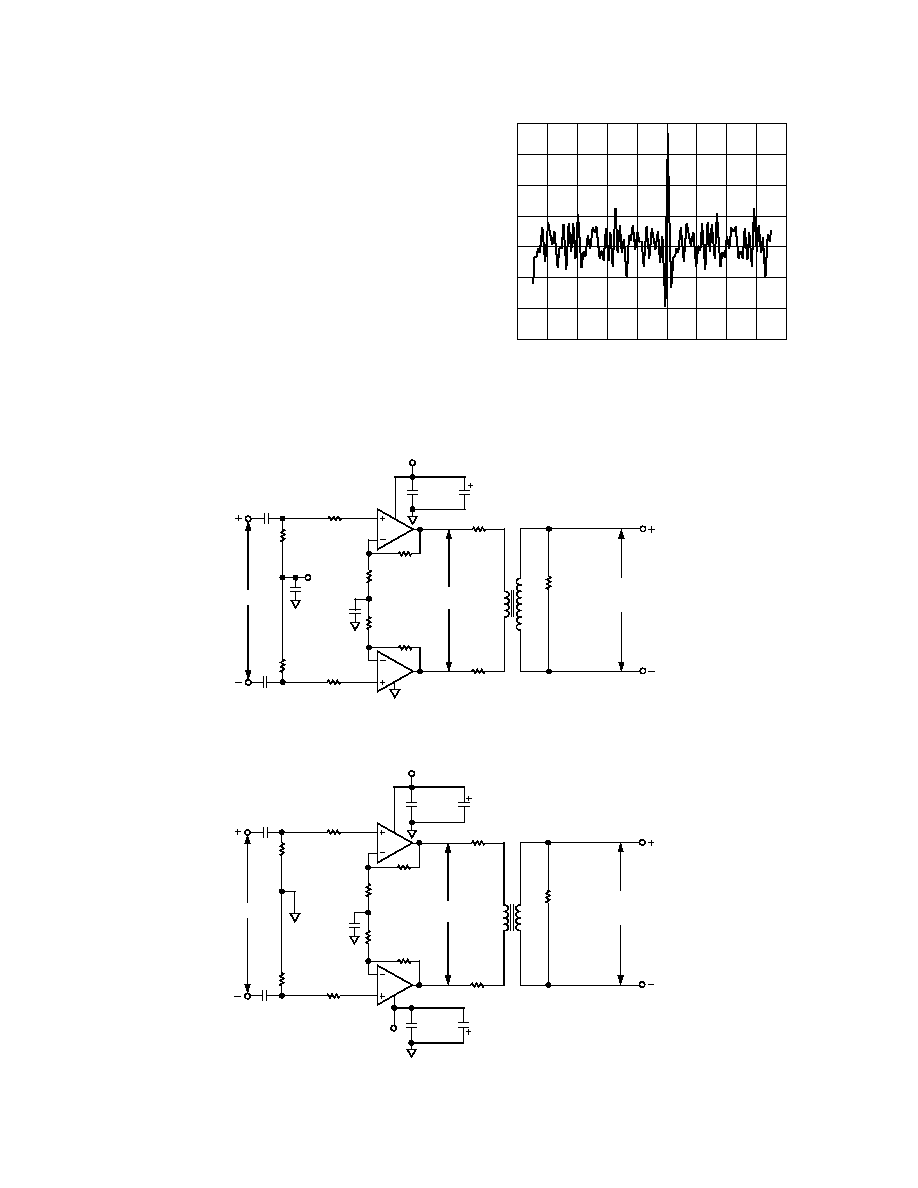
R1
17.3
R
L
= 100
R2
17.3
1:1.7
TRANSFORMER
P
OUT
16dBm
LINE
POWER
13dBm
301
301
50
50
0.1 F
10k
10k
0.1 F
0.1 F
+12V
100
100
0.1 F
V
IN
6V
0.1 F
10 F
Figure 6. Recommended Application Circuit for Single +12 V Supply
R1
12.4
R
L
= 100
R2
12.4
1:1
TRANSFORMER
P
OUT
16dBm
LINE
POWER
13dBm
301
301
50
50
0.1 F
10k
10k
0.1 F
+12V
100
100
0.1 F
V
IN
0.1 F
12V
0.1 F
10 F
10 F
Figure 7. Recommended Application Circuit for
±12 V Supply
0.25
0.15
0.05
0
TIME ms
0.10
0.15
0.20
VOLTS
3
2
1
0
1
2
3
4
0.05
0.10
0.20
Figure 5. DMT Signal in the Time Domain
Generating DMT Signals
At this time, DMT-modulated waveforms are not typically
menu-selectable items contained within arbitrary waveform
generators. Even using (AWG) software to generate DMT sig-
nals, AWGs that are available today may not deliver DMT
signals sufficient in performance with regard to MTPR due to
limitations in the D/A converters and output drivers used by
AWG manufacturers. Similar to evaluating single-tone distor-
tion performance of an amplifier, MTPR evaluation requires a
DMT signal generator capable of delivering MTPR performance
better than that of the driver under evaluation. Generating
DMT signals can be accomplished using a Tektronics AWG
2021 equipped with Option 4, (12-/24-bit, TTL Digital Data
Out), digitally coupled to Analog Devices' AD9754, a 14-bit
TxDAC
®
, buffered by an AD8002 amplifier configured as a
differential driver. Note that the DMT waveforms, available on
the Analog Devices website, www.analog.com, or similar. WFM
files are needed to produce the necessary digital data required to
drive the TxDAC from the optional TTL Digital Data output of
the TEK AWG2021.
TxDAC is a registered trademark of Analog Devices, Inc.
REV. 0
AD8019
15
B
3
2
1
JP3
P4 1
+V
V
U1
1
2
3
4
5
13
VCC
VEE
V
+V
U1
5
3
13
AD8019
AD8019
11
12
10
1
2
A
B
2
JP7
VCC-2
C5
0.1
F
R28
DNI
TP6
R20
DNI
TP7
PR1
A
C11
DNI
C22
DNI
R3
DNI
R1
100
1WATT
R38
DNI
R8
100
C8
0.1
F
TP10
R24
10k
R40
DNI
C28
DNI
R29
10k
R41
DNI
R14
100
C27
DNI
R4
DNI
R21
DNI
C12
DNI
R39
DNI
R37
DNI
PR2
TP9
B
TP8
R30
0
VCC
2
B
JP4
3
1
A
P4 2
P4 3
S5
S6
VCC
VCC
S3
P3 1
P3 2
P3 3
U2
U2
AD8022
AD8022
S4
B
3
2
1
JP6
A
TB1 2
TB1 3
TB1 1
+
+
DNI
R35
DNI
C29
DNI
R36
DNI
C7
DNI
C9
DNI
R32
100
NC = 5,6
T1
1
2
3
4
7
8
9
10
TP1
C6
DNI
P1
1
2
3
4
78
5
6
TP2
TP23
TP24
TP25
TP26
VCCIN
L5
BEAD
L1
BEAD
C4
10
F
25V
C21
0.1
F
C20
0.1
F
C17
DNI
U1 DECOUPLING
U1 DECOUPLING
U2 DECOUPLING
U2 DECOUPLING
C23
DNI
TP19
TP12
C15
0.01
F
C14
10
F
25V
C26
0.1
F
VCC
VEE
JP5
C18
DNI
TP4
TP5
VCC-2
C3
DNI
C16
DNI
R22
DNI
R13
DNI
R10
DNI
R9
DNI
C2
DNI
R23
DNI
C1
DNI
R5
DNI
R6
DNI
VCC
R7
DNI
R34
DNI
R33
DNI
R12
DNI
VCC;8
VEE;4
VCC;8
VEE;4
7
5
6
1
2
3
TP18
TP17
VCC-2
C19
0.1
F
R17
5k
R16
5k
TP3
TP11
C10
0.1
F
VEE
R15
50
R31
0
A
R42
DNI
R2
50
R18
301
C13
0.1
F
R19
301
A
R11
50
*
DNI : DO NOT INSTALL
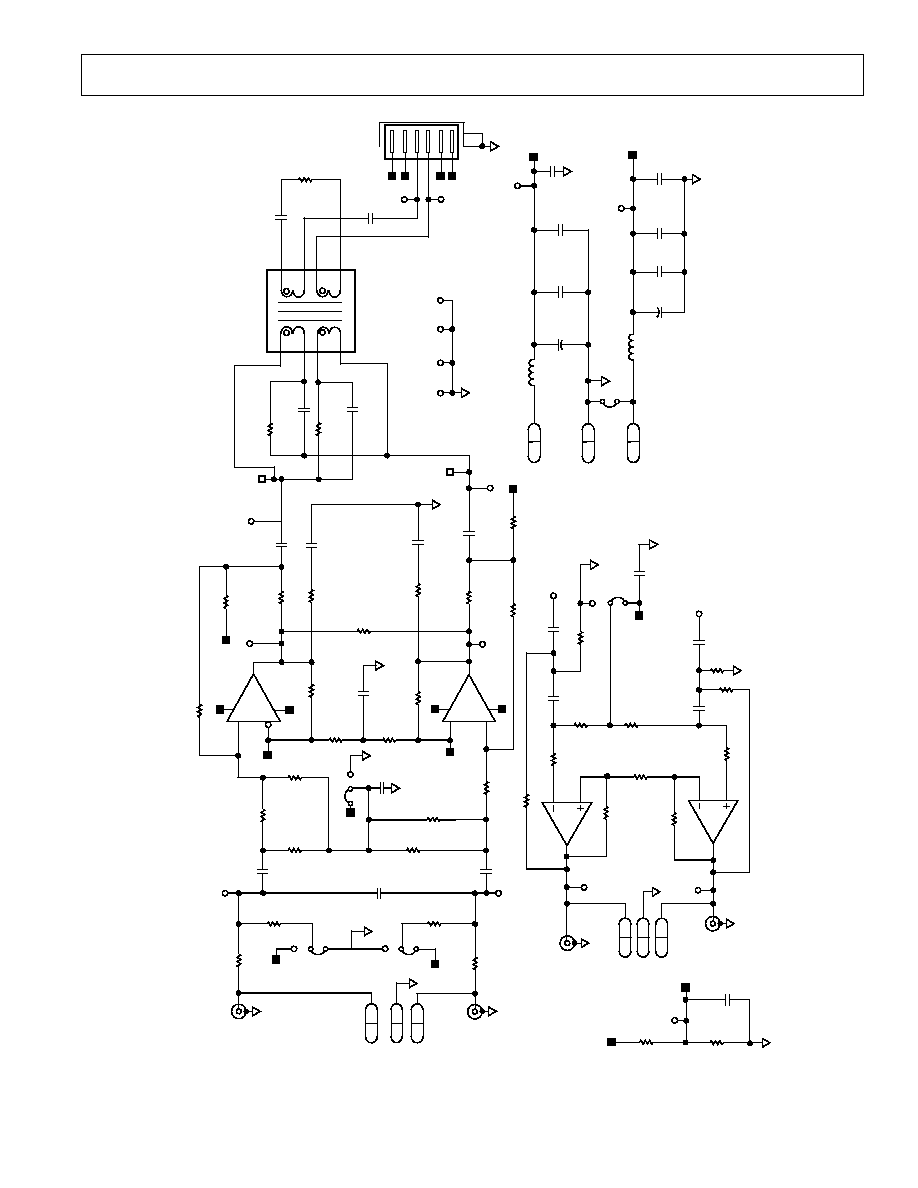
Figure 8. TSSOP Noninverting DSL Evaluation Board Schematic
REV. 0
AD8019
16
VCC
R25
VAL
R26
VAL
R27
VAL
C24
VAL
NC4
NC1
NC2 NC3
1
7
14
8
9
6
1
2
3
B
JP1
PWDN
DGND
U1
AD8019
A
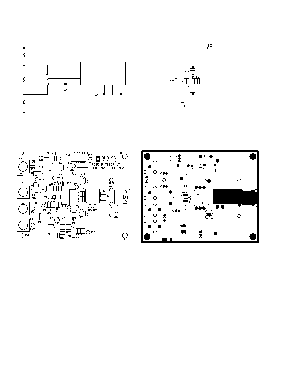
Figure 9. DSL Driver Input Control Circuit
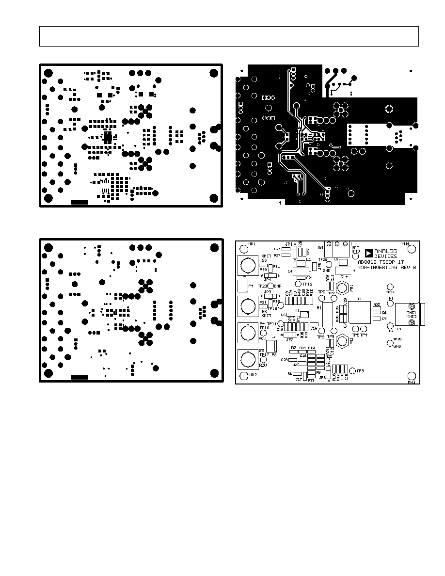
Figure 10. TSSOP Evaluation Board Silkscreen Top
Figure 11. TSSOP Evaluation Board Silkscreen Bottom
2
AGND
AGND
Figure 12. TSSOP Evaluation Board Power Plane
REV. 0
AD8019
17
Figure 13. Solder Mask Top
Figure 14. Solder Mask Bottom
Figure 15. Ground Plane Bottom
Figure 16. Assembly Top
REV. 0
AD8019
18
Figure 17. Ground Plane Top
Figure 18. Assembly Bottom
REV. 0
AD8019
19
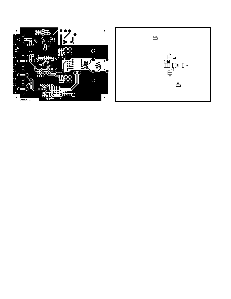
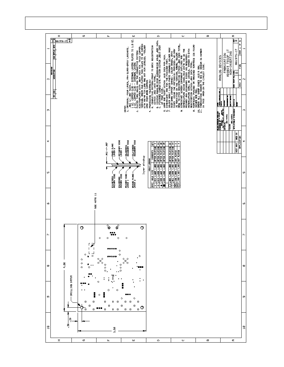
Figure 19. Board Fabrication
REV. 0
20
AD8019
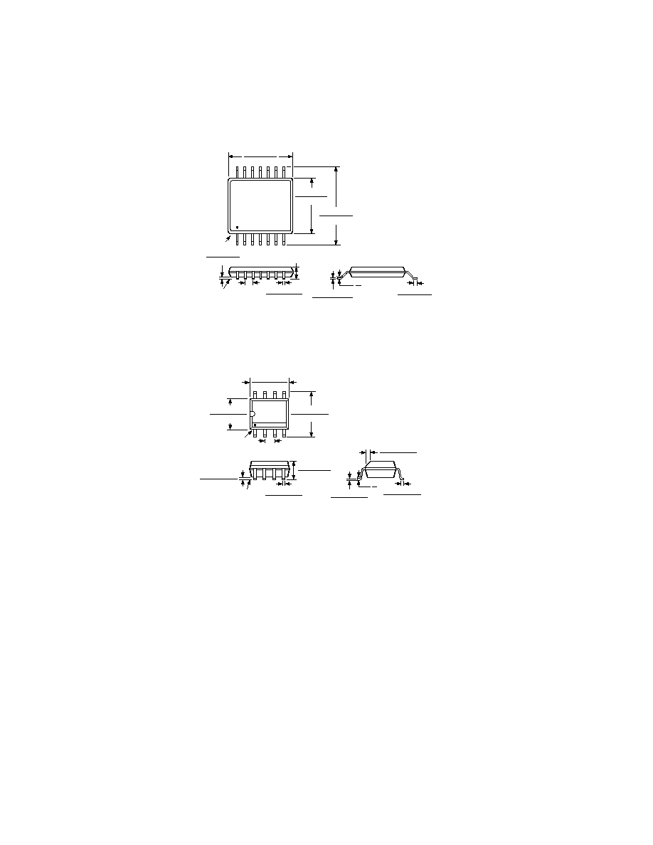
OUTLINE DIMENSIONS
Dimensions shown in inches and (mm).
14-Lead TSSOP
(RU-14)
14
8
7
1
0.256 (6.50)
0.246 (6.25)
0.177 (4.50)
0.169 (4.30)
PIN 1
0.201 (5.10)
0.193 (4.90)
SEATING
PLANE
0.006 (0.15)
0.002 (0.05)
0.0118 (0.30)
0.0075 (0.19)
0.0256
(0.65)
BSC
0.0433 (1.10)
MAX
0.0079 (0.20)
0.0035 (0.090)
0.028 (0.70)
0.020 (0.50)
8
0
8-Lead SOIC
(R-8)
0.0098 (0.25)
0.0075 (0.19)
0.0500 (1.27)
0.0160 (0.41)
0.0196 (0.50)
0.0099 (0.25)
45
8
0
0.102 (2.59)
0.094 (2.39)
SEATING
PLANE
0.0098 (0.25)
0.0040 (0.10)
0.0192 (0.49)
0.0138 (0.35)
8
5
4
1
0.1968 (5.00)
0.1890 (4.80)
PIN 1
0.1574 (4.00)
0.1497 (3.80)
0.0500 (1.27)
BSC
0.2440 (6.20)
0.2284 (5.80)
C025511.54/01(0)
PRINTED IN U.S.A.
Document Outline
- Specifications
- Pinout
- Package drawings
- Ordering Guide
- Features
- Applications
- Product Description
- Absolute Maximum Ratings
- Typical Characteristics
- CAUTION
- POWER-DOWN FEATURE
- POWER SUPPLY AND DECOUPLING
- POWER DISSIPATION
- LAYOUT CONSIDERATIONS
- DIAGRAMS
- TPC 1. Single-Ended Test Circuit; G = +5
- TPC 4. Differential Test Circuit; G = +10
- Simplified Differential Driver
- Recommended Application Circuit for Single +12 V Supply
- Recommended Application Circuit for ± 12 V Supply
- TSSOP Noninverting DSL Evaluation Board Schematic
- DSL Driver Input Control Circuit
- TSSOP Evaluation Board Silkscreen Bottom
- TSSOP Evaluation Board Silkscreen Top
- TSSOP Evaluation Board Power Plane
- Solder Mask Top
- Ground Plane Bottom
- Solder Mask Bottom
- Assembly Top
- Ground Plane Top
- Assembly Bottom
- Board Fabrication