 | ÐлекÑÑоннÑй компоненÑ: AD8021ARM | СкаÑаÑÑ:  PDF PDF  ZIP ZIP |
Äîêóìåíòàöèÿ è îïèñàíèÿ www.docs.chipfind.ru
REV. D
Information furnished by Analog Devices is believed to be accurate and
reliable. However, no responsibility is assumed by Analog Devices for its
use, nor for any infringements of patents or other rights of third parties that
may result from its use. No license is granted by implication or otherwise
under any patent or patent rights of Analog Devices. Trademarks and
registered trademarks are the property of their respective owners.
One Technology Way, P.O. Box 9106, Norwood, MA 02062-9106, U.S.A.
Tel: 781/329-4700
www.analog.com
Fax: 781/326-8703
© 2003 Analog Devices, Inc. All rights reserved.
AD8021
Low Noise, High Speed Amplifier
for 16-Bit Systems
FEATURES
Low Noise
2.1 nV/
Hz Input Voltage Noise
2.1 pA/
Hz Input Current Noise
Custom Compensation
Constant Bandwidth from G = 1 to G = 10
High Speed
200 MHz (G = 1)
190 MHz (G = 10)
Low Power
34 mW or 6.7 mA Typ for 5 V Supply
Output Disable Feature, 1.3 mA
Low Distortion
93 dB Second Harmonic, f
C
= 1 MHz
108 dB Third Harmonic, f
C
= 1 MHz
DC Precision
1 mV Max Input Offset Voltage
0.5 V/ C Input Offset Voltage Drift
Wide Supply Range, 5 V to 24 V
Low Price
Small Packaging
Available in SOIC-8 and MSOP-8
APPLICATIONS
ADC Preamp and Driver
Instrumentation Preamp
Active Filters
Portable Instrumentation
Line Receivers
Precision Instruments
Ultrasound Signal Processing
High Gain Circuits
PRODUCT DESCRIPTION
The AD8021 is a very high performance, high speed voltage
feedback amplifier that can be used in 16-bit resolution systems.
It is designed to have low voltage and current noise (2.1 nV/
Hz
typ and 2.1 pA/
Hz typ) while operating at the lowest quiescent
supply current (7 mA @
±5 V) among today's high speed, low
noise op amps. The AD8021 operates over a wide range of
supply voltages from
± 2.5 V to ± 12 V, as well as from single
5 V supplies, making it ideal for high speed, low power instru-
ments. An output disable pin allows further reduction of the
quiescent supply current to 1.3 mA.
The AD8021 allows the user to choose the gain bandwidth
product that best suits the application. With a single capacitor,
the user can compensate the AD8021 for the desired gain with
little trade-off in bandwidth. The AD8021 is a very well behaved
amplifier that settles to 0.01% in 23 ns for a 1 V step. It has a fast
overload recovery of 50 ns.
The AD8021 is stable over temperature with low input offset
voltage drift and input bias current drift, 0.5
µV/°C and 10 nA/°C,
respectively. The AD8021 is also capable of driving a 75
line
with
±3 V video signals.
The AD8021 is not only technically superior, but also priced
considerably less than comparable amps drawing much higher
quiescent current. The AD8021 is a high speed, general-purpose
amplifier, ideal for a wide variety of gain configurations, and can
be used throughout a signal processing chain and in control loops.
The AD8021 is available in both standard 8-lead SOIC and MSOP
packages in the industrial temperature range of 40
°C to +85°C.
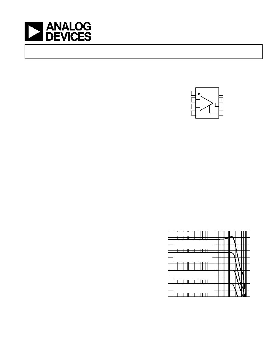
FREQUENCY Hz
0.1M
1G
1M
10M
100M
CLOSED-LOOP GAIN dB
24
21
6
18
15
12
9
6
3
0
3
V
OUT
= 50mV p-p
G = 5, R
F
= 1k , R
G
= 200 ,
R
IN
= 66.5 , C
C
= 1.5pF
G = 2, R
F
=
499 , R
G
= 249 ,
R
IN
= 63.4 , C
C
= 4pF
G = 1, R
F
=
499 , R
G
= 499 ,
R
IN
= 56.2 , C
C
= 7pF
G = 10, R
F
=
1k , R
G
= 100 ,
R
IN
= 100 , C
C
= 0pF
Figure 1. Small Signal Frequency Response
CONNECTION DIAGRAM
SOIC-8 (R-8)
MSOP-8 (RM-8)
8
7
6
5
1
2
3
4
LOGIC
REFERENCE
IN
+IN
V
S
DISABLE
+V
S
V
OUT
C
COMP
AD8021

REV. D
2
AD8021SPECIFICATIONS
(@ T
A
= 25 C, V
S
= 5 V, R
L
= 1 k
, Gain = +2, unless otherwise noted.)
V
S
= 5 V
AD8021AR/AD8021ARM
Parameter
Conditions
Min
Typ
Max
Unit
DYNAMIC PERFORMANCE
3 dB Small Signal Bandwidth
G = +1, C
C
= 10 pF, V
O
= 0.05 V p-p
355
490
MHz
G = +2, C
C
= 7 pF, V
O
= 0.05 V p-p
160
205
MHz
G = +5, C
C
= 2 pF, V
O
= 0.05 V p-p
150
185
MHz
G = +10, C
C
= 0 pF, V
O
= 0.05 V p-p
110
150
MHz
Slew Rate, 1 V Step
G = +1, C
C
= 10 pF
95
120
V/
µs
G = +2, C
C
= 7 pF
120
150
V/
µs
G = +5, C
C
= 2 pF
250
300
V/
µs
G = +10, C
C
= 0 pF
380
420
V/
µs
Settling Time to 0.01%
V
O
= 1 V Step, R
L
= 500
23
ns
Overload Recovery (50%)
±2.5 V Input Step, G = +2
50
ns
DISTORTION/NOISE PERFORMANCE
f = 1 MHz
HD2
V
O
= 2 V p-p
93
dBc
HD3
V
O
= 2 V p-p
108
dBc
f = 5 MHz
HD2
V
O
= 2 V p-p
70
dBc
HD3
V
O
= 2 V p-p
80
dBc
Input Voltage Noise
f = 50 kHz
2.1
2.6
nV/
Hz
Input Current Noise
f = 50 kHz
2.1
pA/
Hz
Differential Gain Error
NTSC, R
L
= 150
0.03
%
Differential Phase Error
NTSC, R
L
= 150
0.04
Degrees
DC PERFORMANCE
Input Offset Voltage
0.4
1.0
mV
Input Offset Voltage Drift
T
MIN
to T
MAX
0.5
µV/°C
Input Bias Current
+Input or Input
7.5
10.5
µA
Input Bias Current Drift
10
nA/
°C
Input Offset Current
0.1
0.5
±µA
Open-Loop Gain
82
86
dB
INPUT CHARACTERISTICS
Input Resistance
10
M
Common-Mode Input Capacitance
1
pF
Input Common-Mode Voltage Range
4.1 to +4.6
V
Common-Mode Rejection Ratio
V
CM
=
±4 V
86
98
dB
OUTPUT CHARACTERISTICS
Output Voltage Swing
3.5 to +3.2
3.8 to +3.4
V
Linear Output Current
60
mA
Short-Circuit Current
75
mA
Capacitive Load Drive for 30% Overshoot
V
O
= 50 mV p-p/1 V p-p
15/120
pF
DISABLE CHARACTERISTICS
Off Isolation
f = 10 MHz
40
dB
Turn-On Time
V
O
= 0 V to 2 V, 50% Logic to 50% Output
45
ns
Turn-Off Time
V
O
= 0 V to 2 V, 50% Logic to 50% Output
50
ns
DISABLE Voltage--Off/On
V
DISABLE
V
LOGIC REFERENCE
1.75/1.90
V
Enabled Leakage Current
Logic Ref = 0.4 V
70
µA
DISABLE = 4.0 V
2
µA
Disabled Leakage Current
Logic Ref = 0.4 V
30
µA
DISABLE = 0.4 V
33
µA
POWER SUPPLY
Operating Range
±2.25
±5
±12.0
V
Quiescent Current
Output Enabled
7.0
7.7
mA
Output Disabled
1.3
1.6
mA
+Power Supply Rejection Ratio
V
CC
= +4 V to +6 V, V
EE
= 5 V
86
95
dB
Power Supply Rejection Ratio
V
CC
= +5 V, V
EE
= 6 V to 4 V
86
95
dB
Specifications subject to change without notice.

REV. D
AD8021
3
AD8021AR/AD8021ARM
Parameter
Conditions
Min
Typ
Max
Unit
DYNAMIC PERFORMANCE
3 dB Small Signal Bandwidth
G = +1, C
C
= 10 pF, V
O
= 0.05 V p-p
520
560
MHz
G = +2, C
C
= 7 pF, V
O
= 0.05 V p-p
175
220
MHz
G = +5, C
C
= 2 pF, V
O
= 0.05 V p-p
170
200
MHz
G = +10, C
C
= 0 pF, V
O
= 0.05 V p-p
125
165
MHz
Slew Rate, 1 V Step
G = +1, C
C
= 10 pF
105
130
V/
µs
G = +2, C
C
= 7 pF
140
170
V/
µs
G = +5, C
C
= 2 pF
265
340
V/
µs
G = +10, C
C
= 0 pF
400
460
V/
µs
Settling Time to 0.01%
V
O
= 1 V Step, R
L
= 500
21
ns
Overload Recovery (50%)
±6 V Input Step, G = +2
90
ns
DISTORTION/NOISE PERFORMANCE
f = 1 MHz
HD2
V
O
= 2 V p-p
95
dBc
HD3
V
O
= 2 V p-p
116
dBc
f = 5 MHz
HD2
V
O
= 2 V p-p
71
dBc
HD3
V
O
= 2 V p-p
83
dBc
Input Voltage Noise
f = 50 kHz
2.1
2.6
nV/
Hz
Input Current Noise
f = 50 kHz
2.1
pA/
Hz
Differential Gain Error
NTSC, R
L
= 150
0.03
%
Differential Phase Error
NTSC, R
L
= 150
0.04
Degrees
DC PERFORMANCE
Input Offset Voltage
0.4
1.0
mV
Input Offset Voltage Drift
T
MIN
to T
MAX
0.2
µV/°C
Input Bias Current
+Input or Input
8
11.3
µA
Input Bias Current Drift
10
nA/
°C
Input Offset Current
0.1
0.5
±µA
Open-Loop Gain
84
88
dB
INPUT CHARACTERISTICS
Input Resistance
10
M
Common-Mode Input Capacitance
1
pF
Input Common-Mode Voltage Range
11.1 to +11.6
V
Common-Mode Rejection Ratio
V
CM
=
±10 V
86
96
dB
OUTPUT CHARACTERISTICS
Output Voltage Swing
10.2 to +9.8
10.6 to +10.2
V
Linear Output Current
70
mA
Short-Circuit Current
115
mA
Capacitive Load Drive for 30% Overshoot
V
O
= 50 mV p-p/1 V p-p
15/120
pF
DISABLE CHARACTERISTICS
Off Isolation
f = 10 MHz
40
dB
Turn-On Time
V
O
= 0 V to 2 V, 50% Logic to 50% Output
45
ns
Turn-Off Time
V
O
= 0 V to 2 V, 50% Logic to 50% Output
50
ns
DISABLE Voltage--Off/On
V
DISABLE
V
LOGIC REFERENCE
1.80/1.95
V
Enabled Leakage Current
Logic Ref = 0.4 V
70
µA
DISABLE = 4.0 V
2
µA
Disabled Leakage Current
Logic Ref = 0.4 V
30
µA
DISABLE= 0.4 V
33
µA
POWER SUPPLY
Operating Range
±2.25
±5
±12.0 V
Quiescent Current
Output Enabled
7.8
8.6
mA
Output Disabled
1.7
2.0
mA
+Power Supply Rejection Ratio
V
CC
= +11 V to +13 V, V
EE
= 12 V
86
96
dB
Power Supply Rejection Ratio
V
CC
= +12 V, V
EE
= 13 V to 11 V
86
100
dB
Specifications subject to change without notice.
(@ T
A
= 25 C, R
L
= 1 k
, Gain = +2, unless otherwise noted.)
V
S
= 12 V

REV. 0
4
AD8021
(@ T
A
= 25 C, R
L
= 1 k
, Gain = +2, unless otherwise noted.)
AD8021AR/AD8021ARM
Parameter
Conditions
Min
Typ
Max
Unit
DYNAMIC PERFORMANCE
3 dB Small Signal Bandwidth
G = +1, C
C
= 10 pF, V
O
= 0.05 V p-p
270
305
MHz
G = +2, C
C
= 7 pF, V
O
= 0.05 V p-p
155
190
MHz
G = +5, C
C
= 2 pF, V
O
= 0.05 V p-p
135
165
MHz
G = +10, C
C
= 0 pF, V
O
= 0.05 V p-p
95
130
MHz
Slew Rate, 1 V Step
G = +1, C
C
= 10 pF
80
110
V/
µs
G = +2, C
C
= 7 pF
110
140
V/
µs
G = +5, C
C
= 2 pF
210
280
V/
µs
G = +10, C
C
= 0 pF
290
390
V/
µs
Settling Time to 0.01%
V
O
= 1 V Step, R
L
= 500
28
ns
Overload Recovery (50%)
0 V to 2.5 V Input Step, G = +2
40
ns
DISTORTION/NOISE PERFORMANCE
f = 1 MHz
HD2
V
O
= 2 V p-p
84
dBc
HD3
V
O
= 2 V p-p
91
dBc
f = 5 MHz
HD2
V
O
= 2 V p-p
68
dBc
HD3
V
O
= 2 V p-p
81
dBc
Input Voltage Noise
f = 50 kHz
2.1
2.6
nV/
Hz
Input Current Noise
f = 50 kHz
2.1
pA/
Hz
DC PERFORMANCE
Input Offset Voltage
0.4
1.0
mV
Input Offset Voltage Drift
T
MIN
to T
MAX
0.8
µV/°C
Input Bias Current
+Input or Input
7.5
10.3
µA
Input Bias Current Drift
10
nA/
°C
Input Offset Current
0.1
0.5
±µA
Open-Loop Gain
72
76
dB
INPUT CHARACTERISTICS
Input Resistance
10
M
Common-Mode Input Capacitance
1
pF
Input Common-Mode Voltage Range
0.9 to 4.6
V
Common-Mode Rejection Ratio
1.5 V to 3.5 V
84
98
dB
OUTPUT CHARACTERISTICS
Output Voltage Swing
1.25 to 3.38
1.10 to 3.60
V
Linear Output Current
30
mA
Short-Circuit Current
50
mA
Capacitive Load Drive for 30% Overshoot
V
O
= 50 mV p-p/1 V p-p
10/120
pF
DISABLE CHARACTERISTICS
Off Isolation
f = 10 MHz
40
dB
Turn-On Time
V
O
= 0 V to 1 V, 50% Logic to 50% Output
45
ns
Turn-Off Time
V
O
= 0 V to 1 V, 50% Logic to 50% Output
50
ns
DISABLE Voltage--Off/On
V
DISABLE
V
LOGIC REFERENCE
1.55/1.70
V
Enabled Leakage Current
Logic Ref = 0.4 V
70
µA
DISABLE = 4.0 V
2
µA
Disabled Leakage Current
Logic Ref = 0.4 V
30
µA
DISABLE = 0.4 V
33
µA
POWER SUPPLY
Operating Range
±2.25
±5
±12.0 V
Quiescent Current
Output Enabled
6.7
7.5
mA
Output Disabled
1.2
1.5
mA
+Power Supply Rejection Ratio
V
CC
= 4.5 V to 5.5 V, V
EE
= 0 V
74
82
dB
Power Supply Rejection Ratio
V
CC
= +5 V, V
EE
= 0.5 V to +0.5 V
76
84
dB
Specifications subject to change without notice.
V
S
= 5 V
REV. D
AD8021
5
CAUTION
ESD (electrostatic discharge) sensitive device. Electrostatic charges as high as 4000 V readily
accumulate on the human body and test equipment and can discharge without detection. Although the
AD8021 features proprietary ESD protection circuitry, permanent damage may occur on devices
subjected to high energy electrostatic discharges. Therefore, proper ESD precautions are recommended
to avoid performance degradation or loss of functionality.
ABSOLUTE MAXIMUM RATINGS
1
Supply Voltage . . . . . . . . . . . . . . . . . . . . . . . . . . . . . . . . 26.4 V
Power Dissipation . . . . . . . . Observed Power Derating Curves
Input Voltage (Common-Mode) . . . . . . . . . . . . . . .
±V
S
± 1 V
Differential Input Voltage
2
. . . . . . . . . . . . . . . . . . . . . .
±0.8 V
Differential Input Current . . . . . . . . . . . . . . . . . . . . .
±10 mA
Output Short-Circuit Duration
. . . . . . . . . . . . . . . . . . . . . . Observed Power Derating Curves
Storage Temperature . . . . . . . . . . . . . . . . . . 65
C to +125C
Operating Temperature Range . . . . . . . . . . . 40
C to +85C
Lead Temperature Range (Soldering, 10 sec) . . . . . . . . 300
C
NOTES
1
Stresses above those listed under Absolute Maximum Ratings may cause perma-
nent damage to the device. This is a stress rating only and functional operation of
the device at these or any other conditions above those indicated in the operational
section of this specification is not implied. Exposure to absolute maximum rating
conditions for extended periods may affect device reliability.
2
The AD8021 inputs are protected by diodes. Current-limiting resistors are not
used in order to preserve the low noise. If a differential input exceeds
±0.8 V, the
input current should be limited to
±10 mA.
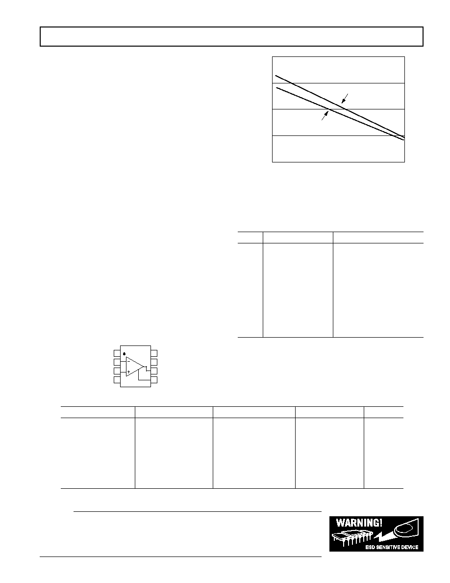
MAXIMUM POWER DISSIPATION
The maximum power that can be safely dissipated by the AD8021
is limited by the associated rise in junction temperature. The maxi-
mum safe junction temperature for plastic encapsulated devices
is determined by the glass transition temperature of the plastic,
approximately 150
C. Temporarily exceeding this limit may cause
a shift in parametric performance due to a change in the stresses
exerted on the die by the package. Exceeding a junction tempera-
ture of 175
C for an extended period can result in device failure.
While the AD8021 is internally short-circuit protected, this may
not be sufficient to guarantee that the maximum junction tem-
perature (150
C) is not exceeded under all conditions. To ensure
proper operation, it is necessary to observe the maximum power
derating curves.
PIN CONFIGURATION
8
7
6
5
1
2
3
4
LOGIC
REFERENCE
IN
+IN
V
S
DISABLE
+V
S
V
OUT
C
COMP
AD8021
AMBIENT TEMPERATURE ( C)
MAXIMUM POWER DISSIPATION (mW)
2.0
1.5
1.0
0.5
0.01
55 45 35 25 15 5 5 15 25 35 45
55
65 75
85
8-LEAD SOIC
8-LEAD MSOP
Figure 2. Maximum Power Dissipation vs. Temperature*
*Specification is for device in free air:
8-Lead SOIC:
JA
= 125
C/W
8-Lead MSOP:
JA
= 145
C/W
PIN FUNCTION DESCRIPTIONS
Pin No. Mnemonic
Function
1
LOGIC REFERENCE Reference for Pin 8
* Voltage
Level. Connect to logic low
supply.
2
IN
Inverting Input
3
+IN
Noninverting Input
4
V
S
Negative Supply Voltage
5
C
COMP
Compensation Capacitor. Tie
to V
S
. (See the Applications
section for value.)
6
V
OUT
Output
7
+V
S
Positive Supply Voltage
8
DISABLE
Disable, Active Low
*
*When Pin 8 (DISABLE) is about 2 V or more higher than Pin 1 (LOGIC
REFERENCE), the part is enabled. When Pin 8 is brought down to within about
1.5 V of Pin 1, the part is disabled. (See the Specification tables for exact disable and
enable voltage levels.) If the disable feature is not going to be used, Pin 8 can be tied
to +V
S
or a logic high source, and Pin 1 can be tied to ground or logic low. Alterna-
tively, if Pin 1 and Pin 8 are not connected, the part will be in an enabled state.
ORDERING GUIDE
Model
Temperature Range
Package Description
Package Outline
Branding
AD8021AR
40
C to +85C
8-Lead SOIC
R-8
AD8021AR-REEL
40
C to +85C
8-Lead SOIC
R-8
AD8021AR-REEL7
40
C to +85C
8-Lead SOIC
R-8
AD8021ARM
40
C to +85C
8-Lead MSOP
RM-8
HNA
AD8021ARM-REEL
40
C to +85C
8-Lead MSOP
RM-8
HNA
AD8021ARM-REEL7
40
C to +85C
8-Lead MSOP
RM-8
HNA
AD8021ARZ
*
40
C to +85C
8-Lead SOIC
R-8
AD8021ARZ-REEL
*
40
C to +85C
8-Lead SOIC
R-8
AD8021ARZ-REEL7
*
40
C to +85C
8-Lead SOIC
R-8
*Z = Lead Free
Document Outline
- FEATURES
- CONNECTION DIAGRAM
- PRODUCT DESCRIPTION
- SPECIFICATIONS
- VS = ±5 V
- VS = ±12 V
- VS = 5 V
- ABSOLUTE MAXIMUM RATINGS
- MAXIMUM POWER DISSIPATION
- PIN CONFIGURATION
- PIN FUNCTION DESCRIPTIONS
- ORDERING GUIDE
- Typical Performance Characteristics
- Test Circuits
- APPLICATIONS
- Using the Disable Feature
- THEORY OF OPERATION
- PCB LAYOUT CONSIDERATIONS
- DRIVING 16-BIT ADCS
- DIFFERENTIAL DRIVER
- USING THE AD8021 IN ACTIVE FILTERS
- OUTLINE DIMENSIONS
- Revision History