 | ÐлекÑÑоннÑй компоненÑ: AD8022 | СкаÑаÑÑ:  PDF PDF  ZIP ZIP |
Äîêóìåíòàöèÿ è îïèñàíèÿ www.docs.chipfind.ru
REV. 0
Information furnished by Analog Devices is believed to be accurate and
reliable. However, no responsibility is assumed by Analog Devices for its
use, nor for any infringements of patents or other rights of third parties
which may result from its use. No license is granted by implication or
otherwise under any patent or patent rights of Analog Devices.
a
AD8022
One Technology Way, P.O. Box 9106, Norwood, MA 02062-9106, U.S.A.
Tel: 781/329-4700
World Wide Web Site: http://www.analog.com
Fax: 781/326-8703
© Analog Devices, Inc., 1999
Dual High-Speed
Low-Noise Op Amps
FUNCTIONAL BLOCK DIAGRAM
8
7
6
5
1
2
3
4
OUT1
IN1
+IN1
V
S
+V
S
OUT2
IN2
+IN2
AD8022
+
+
FEATURES
Low-Noise Amplifiers Provide Low Noise and Low
Distortion, Ideal for xDSL Modem Receiver
+5 V to 12 V Voltage Supply
Low-Power Consumption
4.0 mA/Amp (Typ) Supply Current
Voltage Feedback Amplifiers
Low Noise and Distortion
2.5 nV/
Hz Voltage Noise @ 100 kHz
SFDR 95 dBc @ 1 MHz
MTPR < 66 dBc
High Speed
120 MHz Bandwidth (3 dB), G = 1
50 V/ s Slew Rate
Low-Offset Voltage, 1.5 mV Typical
APPLICATIONS
ADSL, VDSL, HDSL, and Proprietary xDSL Systems
Low-Noise Instrumentation Front End
Ultrasound Preamp
PRODUCT DESCRIPTION
The AD8022 consists of two low-noise, high-speed, voltage feed-
back amplifiers. Both inputs add only 2.5 nV/
Hz of voltage
noise. These dual amplifiers provide wideband, low-distortion
performance, with high-output current optimized for stability
when driving capacitive loads. Operating from +5 V to
±
12 V
supplies, the AD8022 typically consumes only 4.0 mA/Amp
quiescent current. The AD8022 is available in both an 8-lead
microSOIC and an 8-lead SOIC package. Fast overvoltage
recovery and wide bandwidth make the AD8022 ideal as the
receive channel front end to an ADSL, VDSL or proprietary
xDSL transceiver design.
Low-noise receive amplifiers in the AD8022 are independent
voltage feedback amplifiers and can be configured as the differ-
ential receiver from the line transformer or as independent active
filters in an xDSL line interface circuit.
FREQUENCY Hz
3.0
10k
pA AND nV/ Hz
2.5
2.0
1.5
1.0
0.5
0
100k
1M
VOLTAGE NOISE, nV
CURRENT NOISE, pA
Figure 1. Current and Voltage Noise vs. Frequency

2
REV. 0
AD8022SPECIFICATIONS
(@ 25 C, V
S
= 12 V, R
L
= 500
, G = 1, T
MIN
= 40 C, T
MAX
= +85 C, unless
otherwise noted)
Parameter
Conditions
Min
Typ
Max
Unit
DYNAMIC PERFORMANCE
3 dB Small Signal Bandwidth
V
OUT
= 0.2 V p-p
120
MHz
Bandwidth for 0.1 dB Flatness
V
OUT
= 0.2 V p-p
25
MHz
Large Signal Bandwidth
V
OUT
= 4 V p-p
15
MHz
Slew Rate
V
OUT
= 2 V p-p, G = 2
50
V/
µ
s
Rise and Fall Time
V
OUT
= 2 V p-p, G = 2
30
ns
Settling Time 0.1%
V
OUT
= 2 V p-p
62
ns
Overdrive Recovery Time
V
OUT
= 150% of Max Output
Voltage, G = 2
200
ns
NOISE/DISTORTION PERFORMANCE
Distortion
V
OUT
= 2 V p-p
Second Harmonic
f
C
= 1 MHz
95
dBc
Third Harmonic
f
C
= 1 MHz
100
dBc
Multitone Input Power Ratio
1
G = 7 Differential
26 kHz to 132 kHz
67.2
dBc
144 kHz to 1.1 MHz
66
dBc
Voltage Noise (RTI)
f = 100 kHz
2.5
nV/
Hz
Input Current Noise
f = 100 kHz
1.2
pA/
Hz
INPUT CHARACTERISTICS
RTI Offset Voltage
6
1.5
+6
mV
T
MIN
to T
MAX
7.25
+7.25
mV
Input Bias Current
5
+2.5
+5
µ
A
T
MIN
to T
MAX
7.5
+7.5
µ
A
Input Resistance (Differential)
20
k
Input Capacitance
0.7
pF
Input Common-Mode Voltage Range
11.25 to +11.75
V
OUTPUT CHARACTERISTICS
Output Voltage Swing
Single-Ended
10.1
+10.1
V
Short Circuit Output Current
100
mA
Capacitive Load Drive
R
S
= 0
, <3 dB of Peaking
75
pF
POWER SUPPLY
Operating Range
+4.5
±
13.0
V
Quiescent Current
4.0
5.5
mA/Amp
T
MIN
to T
MAX
6.1
mA
Power Supply Rejection Ratio
V
S
=
±
5 V to
±
12 V
80
dB
OPERATING TEMPERATURE RANGE
40
+85
°
C
NOTES
1
Multitone testing performed with 800 mV rms across a 500
load at Points A and B on Figure 17.
Specifications subject to change without notice.

3
REV. 0
AD8022
(@ 25 C, V
S
= 2.5 V, R
L
= 500 , G = 1, T
MIN
= 40 C, T
MAX
= +85 C, unless
otherwise noted)
Parameter
Conditions
Min
Typ
Max
Unit
DYNAMIC PERFORMANCE
3 dB Small Signal Bandwidth
V
OUT
= 0.2 V p-p
94
MHz
Bandwidth for 0.1 dB Flatness
V
OUT
= 0.2 V p-p
22
MHz
Large Signal Bandwidth
V
OUT
= 3 V p-p
10
MHz
Slew Rate
V
OUT
= 2 V p-p, G = 2
42
V/
µ
s
Rise and Fall Time
V
OUT
= 2 V p-p, G = 2
40
ns
Settling Time 0.1%
V
OUT
= 2 V p-p
75
ns
Overdrive Recovery Time
V
OUT
= 150% of Max Output
Voltage, G = 2
225
ns
NOISE/DISTORTION PERFORMANCE
Distortion
V
OUT
= 2 V p-p
Second Harmonic
f
C
= 1 MHz
77.5
dBc
Third Harmonic
f
C
= 1 MHz
94
dBc
Multitone Input Power Ratio
1
G = 7 Differential, V
S
=
±
6 V
26 kHz to 132 kHz
69
dBc
144 kHz to 1.1 MHz
66.7
dBc
Voltage Noise (RTI)
f = 100 kHz
2.3
nV/
Hz
Input Current Noise
f = 100 kHz
1
pA/
Hz
INPUT CHARACTERISTICS
RTI Offset Voltage
5.0
0.8
+5.0
mV
T
MIN
to T
MAX
6.25
+6.25
mV
Input Bias Current
5.0
+2.0
+5.0
µ
A
T
MIN
to T
MAX
7.5
µ
A
Input Resistance (Differential)
20
k
Input Capacitance
0.7
pF
Input Common-Mode Voltage Range
1.83 to +2.5
V
OUTPUT CHARACTERISTICS
Output Voltage Swing
Single-Ended
1.38
+1.48
V
Short Circuit Output Current
80
mA
Capacitive Load Drive
R
S
= 0
, <3 dB of Peaking
75
pF
POWER SUPPLY
Operating Range
+4.5
±
13.0
V
Quiescent Current
3.5
4.25
mA/Amp
T
MIN
to T
MAX
4.4
mA
Power Supply Rejection Ratio
V
S
=
±
1 V
86
dB
OPERATING TEMPERATURE RANGE
40
+85
°
C
NOTES
1
Multitone testing performed with 800 mV rms across a 500
load at Points A and B on Figure 17.
Specifications subject to change without notice.
SPECIFICATIONS
AD8022
4
REV. 0
ORDERING GUIDE
Temperature
Package
Package
Model
Range
Description
Option
AD8022AR
40
°
C to +85
°
C
8-Lead Plastic SOIC
SO-8
AD8022ARM
40
°
C to +85
°
C
8-Lead microSOIC
RM-8
AD8022AR-EVAL
Evaluation Board
SO-8
CAUTION
ESD (electrostatic discharge) sensitive device. Electrostatic charges as high as 4000 V readily
accumulate on the human body and test equipment and can discharge without detection. Although
the AD8022 features proprietary ESD protection circuitry, permanent damage may occur on
devices subjected to high-energy electrostatic discharges. Therefore, proper ESD precautions are
recommended to avoid performance degradation or loss of functionality.
WARNING!
ESD SENSITIVE DEVICE
AMBIENT TEMPERATURE C
2.0
50
MAXIMUM POWER DISSIPATION Watts
1.5
1.0
0.5
0
40 30 20 10 0
10
20 30
40 50
60 70
80 90
T
J
= 150 C
8-LEAD SOIC PACKAGE
8-LEAD MICROSOIC
Figure 2. Plot of Maximum Power Dissipation vs.
Temperature
ABSOLUTE MAXIMUM RATINGS
1
Supply Voltage . . . . . . . . . . . . . . . . . . . . . . . . . . . . . . . . . 26 V
Internal Power Dissipation
2
Small Outline Package (R) . . . . . . . . . . . . . . . . . . . . . 1.6 W
microSOIC Package (RM) . . . . . . . . . . . . . . . . . . . . . 1.2 W
Input Voltage (Common Mode) . . . . . . . . . . . . . . . . . . . .
±
V
S
Differential Input Voltage . . . . . . . . . . . . . . . . . . . . . . .
±
0.8 V
Output Short Circuit Duration
. . . . . . . . . . . . . . . . . . . . . . Observe Power Derating Curves
Storage Temperature Range RM, R . . . . . . 65
°
C to +125
°
C
Operating Temperature Range (A Grade) . . . 40
°
C to +85
°
C
Lead Temperature Range (Soldering 10 sec) . . . . . . . . . 300
°
C
NOTES
1
Stresses above those listed under Absolute Maximum Ratings may cause perma-
nent damage to the device. This is a stress rating only; functional operation of the
device at these or any other conditions above those indicated in the operational
section of this specification is not implied. Exposure to absolute maximum rating
conditions for extended periods may affect device reliability.
2
Specification is for the device in free air:
8-Lead SOIC Package:
JA
= 160
°
C/W.
8-Lead microSOIC Package:
JA
= 200
°
C/W.
MAXIMUM POWER DISSIPATION
The maximum power that can be safely dissipated by the AD8022
is limited by the associated rise in junction temperature. The
maximum safe junction temperature for plastic encapsulated
devices is determined by the glass transition temperature of the
plastic, approximately 150
°
C. Temporarily exceeding this limit
may cause a shift in parametric performance due to a change
in the stresses exerted on the die by the package. Exceeding a
junction temperature of 175
°
C for an extended period can result
in device failure.
While the AD8022 is internally short circuit protected, this may not
be sufficient to guarantee that the maximum junction temperature
(150
°
C) is not exceeded under all conditions. To ensure proper
operation, it is necessary to observe the maximum power derat-
ing curves.
AD8022
5
REV. 0
FREQUENCY MHz
5
4
3
2
1
0
1
2
3
4
5
1
10
100
500
V
IN
= 0.05V p-p
V
IN
= 0.2V p-p
V
IN
= 0.4V p-p
V
IN
= 0.8V p-p
V
IN
= 2V p-p
V
IN
V
OUT
50
56.2
453
402
+
0.1
dB
Figure 3. Frequency Response vs. Signal Level,
V
S
=
±
12 V, G = 1
FREQUENCY Hz
0.4
100k
dB
0.3
0.2
0.1
0
0.1
0.2
0.3
0.4
0.5
0.6
1M
10M
100M
G = 1
R
L
= 509V
12V
5.0V
2.5V
Figure 4. Fine-Scale Gain Flatness vs. Frequency, G = 1
SUPPLY VOLTAGE Volts
140
0
0
14
2
FREQUENCY MHz
4
6
8
10
12
120
80
60
40
20
100
G = +1, R
F
= 402
G = +2, R
F
= 715
Figure 5. Bandwidth vs. Supply, R
L
= 500
, V
IN
= 10 dBm
FREQUENCY MHz
dB
0.1
10
100
500
1
5
4
3
2
1
0
1
2
3
4
5
50
50
50
R
F
+
R
F
= 402
R
F
= 0
R
F
= 715
V
IN
V
OUT
Figure 6. Frequency Response vs. R
F
, G = 1, V
S
=
±
12 V,
V
IN
= 22 dBm
FREQUENCY Hz
0.4
100k
dB
0.3
0.2
0.1
0
0.1
0.2
0.3
0.4
0.5
0.6
1M
10M
100M
G = 2
R
L
= 509V
12V
5.0V
2.5V
Figure 7. Fine-Scale Gain Flatness vs. Frequency, G = 2
SUPPLY VOLTAGE Volts
70
2.5
SLEW RATE V/
s
60
50
40
30
20
10
0
4.5
6.5
8.5
10.5
12.5
NEGATIVE EDGE
POSITIVE EDGE
Figure 8. Slew Rate vs. Supply Voltage, V
S
=
±
12 V, G = 2
AD8022
6
REV. 0
100mV
100
90
10
0%
100ns
100mV
INPUT
OUTPUT
Figure 9. Noninverting Small Signal Pulse Response,
R
L
= 500
, V
S
=
±
12 V, G = 1, R
F
= 0
2.00V
100
90
10
0%
100ns
2.00V
INPUT
OUTPUT
Figure 10. Noninverting Large Signal Pulse Response,
R
L
= 500
, V
S
=
±
12 V, G = 1, R
F
= 0
TIME ns
0.4
SETTLING TIME %
0
0.3
0.2
0.1
0
0.1
0.2
0.3
0.4
40
60
80
100
120
20
+0.1%
0.1%
Figure 11. Settling Time to 0.1%, V
S
=
±
12 V,
Step Size = 2 V p-p, G = 2, R
L
= 500
100mV
100
90
10
0%
100ns
100mV
INPUT
OUTPUT
Figure 12. Noninverting Small Signal Pulse Response,
R
L
= 500
, V
S
=
±
2.5 V, G = 1, R
F
= 0
1.00V
100
90
10
0%
100ns
1.00V
INPUT
OUTPUT
Figure 13. Noninverting Large Signal Pulse Response,
R
L
= 500
, V
S
=
±
2.5 V, G = 1, R
F
= 0
TIME ns
0.4
SETTLING TIME %
0
0.3
0.2
0.1
0
0.1
0.2
0.3
0.4
40
60
80
100
120
20
+0.1%
0.1%
Figure 14. Settling Time to 0.1%, V
S
=
±
2.5 V,
Step Size = 2 V p-p, G = 2, R
L
= 500
AD8022
7
REV. 0
OUTPUT VOLTAGE Volts p-p
20
0
HARMONIC DISTORTION dBc
30
40
50
60
70
80
90
100
120
5
10
15
20
3RD
2ND
Figure 15. Distortion vs. Output Voltage, V
S
=
±
12 V,
G = 2, f = 1 MHz, R
L
= 500
, R
F
= 715
FREQUENCY Hz
HARMONIC DISTORTION dB
60
70
80
90
100
10k
100k
1M
1k
110
120
130
50
2ND
3RD
Figure 16. Distortion vs. Frequency, V
S
=
±
12 V,
R
L
= 500
, R
F
= 715
, V
OUT
= 2 V p-p, Gain = 1
250
715
715
500
+V
V
AD8022
1/2
AD8022
1/2
Figure 17. Multitone Power Ratio Test Circuit
OUTPUT VOLTAGE Volts p-p
0
0
HARMONIC DISTORTION dBc
20
40
60
80
100
120
1.0
1.5
2.0
3.0
0.5
2.5
3RD
2ND
Figure 18. Distortion vs. Output Voltage, V
S
=
±
2.5 V,
G = 2, f = 1 MHz, R
L
= 500
, R
F
= 715
FREQUENCY Hz
HARMONIC DISTORTION dB
60
70
80
90
100
10k
100k
1M
1k
110
120
130
50
2ND
3RD
Figure 19. Distortion vs. Frequency, V
S
=
±
2.5 V,
R
L
= 500
, R
F
= 715
, V
OUT
= 2 V p-p, Gain = 1
4
3
2
1
0
1
2
3
4
12.5
10.0 7.5
5.0
2.5
0
2.5
5.0
7.5
10.0
12.5
V
CM
Volts
V
OS
mV
V
S
= 12V
V
S
= 2.5V
1k
500
V
OUT
V
IN
1k
1k
1k
-
Figure 20. Input Common-Mode Voltage Range
AD8022
8
REV. 0
FREQUENCY kHz
549.3 550.3 551.3 552.3 553.3 554.3 555.3 556.3 557.3 558.3 559.3
10dB/DIV
66.7dBc
Figure 21. Multitone Power Ratio: V
S
=
±
6 V, R
L
= 500
,
Full Rate ADSL (DMT), Downstream
FREQUENCY kHz
549.3 550.3 551.3 552.3 553.3 554.3 555.3 556.3 557.3 558.3 559.3
10dB/DIV
66.0dBc
Figure 22. Multitone Power Ratio: V
S
=
±
12 V, R
L
= 500
,
Full Rate ADSL (DMT), Downstream
TEMPERATURE C
60
4.5
BIAS CURRENT
A
4.0
3.5
3.0
2.5
2.0
1.5
1.0
0.5
0
40
20
0
20
40
60
80
100
120
140
V
S
= 12V
V
S
= 2.5V
Figure 23. Bias Current vs. Temperature
FREQUENCY kHz
102.4 103.4 104.4 105.4 106.4 107.4 108.4 109.4 110.4 111.4 112.4
10dB/DIV
69.0dBc
Figure 24. Multitone Power Ratio: V
S
=
±
6 V, R
L
= 500
,
Full Rate ADSL (DMT), Upstream
FREQUENCY kHz
102.4 103.4 104.4 105.4 106.4 107.4 108.4 109.4 110.4 111.4 112.4
10dB/DIV
67.2dBc
Figure 25. Multitone Power Ratio: V
S
=
±
12 V, R
L
= 500
,
Full Rate ADSL (DMT), Upstream
TEMPERATURE C
8.5
8.0
5.0
50
150
0
SUPPLY CURRENT Total mA
50
100
7.0
6.5
6.0
5.5
7.5
V
S
= 12V
V
S
= 2.5V
Figure 26. Total Supply Current Over Temperature
AD8022
9
REV. 0
FREQUENCY Hz
OUTPUT IMPEDANCE
100
31.6
10
3.16
1
0.316
0.1
0.0316
1M
10M
100M
500M
100k
30k
Figure 27. Output Impedance vs. Frequency, V
S
=
±
12 V
FREQUENCY Hz
0
CROSSTALK dB
10
20
30
40
50
60
70
80
90
100
1M
10M
100M
100k
SIDE A OUT
SIDE B OUT
Figure 28. Output-to-Output Crosstalk vs. Frequency,
V
S
=
±
12 V
FREQUENCY Hz
10
1k
CMRR dB
30
50
70
90
110
10k
100k
1M
604
604
154
56.7
50
154
Figure 29. CMRR vs. Frequency
FREQUENCY kHz
FREQUENCY RESPONSE dB
0.1
10
100
500
1
0pF
30pF
50pF
5
4
3
2
1
0
1
2
3
4
5
50
715
715
C
L
R
S
56.2
453
+
V
IN
V
OUT
Figure 30. Frequency Response vs. Capacitive Load,
C
L
= 0 pF, 30 pF and 50 pF, R
S
= 0
FREQUENCY Hz
0
CROSSTALK dB
10
20
30
40
50
60
70
80
90
100
1M
10M
100M
100k
SIDE A OUT
SIDE B OUT
Figure 31. Output -to-Output Crosstalk vs. Frequency,
V
S
=
±
2.5 V
TEMPERATURE Degrees
0
60
VOLTAGE OFFSET mV
0.5
1.0
1.5
2.0
2.5
20
40
20
0
40
60
80
100
120
140
SIDE B
V
S
= +12V
SIDE A
SIDE A
SIDE B
V
S
= 2.5V
Figure 32. Voltage Offset vs. Temperature
AD8022
10
REV. 0
FREQUENCY Hz
0
10k
POWER SUPPLY REJECTION dB
10
20
30
40
50
60
70
80
90
100
100k
1M
10M
100M
PSRR
+PSRR
Figure 33. Power Supply Rejection vs. Frequency,
V
S
=
±
12 V
FREQUENCY Hz
0
10k
POWER SUPPLY REJECTION dB
10
20
30
40
50
60
70
80
90
100
100k
1M
10M
100M
PSRR
+PSRR
Figure 34. Power Supply Rejection vs. Frequency,
V
S
=
±
2.5 V
THEORY OF OPERATION
The AD8022 is a voltage-feedback op amp designed especially
for ADSL or other applications requiring very low voltage and
current noise along with low-supply current, low distortion, and
ease of use.
The AD8022 is fabricated on Analog Devices' proprietary eXtra-
Fast Complementary Bipolar (XFCB) process, which enables
the construction of PNP and NPN transistors with similar fTs in
the 4 GHz region. The process is dielectrically isolated to eliminate
the parasitic and latch-up problems caused by junction isolation.
These features enable the construction of high-frequency, low-
distortion amplifiers with low-supply currents.
7.5pF
15
15
+V
S
V
S
OUTPUT
+IN
IN
600 A
OFFSET NULL
Figure 35. Simplified Schematic
As shown in Figure 35, the AD8022 input stage consists of an
NPN differential pair in which each transistor operates a 300
µ
A
collector current. This gives the input devices a high transconduc-
tance and hence gives the AD8022 low-input noise of 2.5 nV/
Hz
@ 100 kHz. The input stage drives a folded cascode that consists
of a pair of PNP transistors. These PNP's then drive a current
mirror that provides a differential-input to single-ended-out-
put conversion. The output stage provides a high-current gain
of 10,000, so that the AD8022 can maintain a high-dc open-
loop gain, even into low-load impedances.
APPLICATIONS
The low-noise AD8022 dual xDSL receiver amplifier is specifi-
cally designed for the dual differential receiver amplifier function
within xDSL transceiver hybrids as well as other low-noise
amplifier applications. The AD8022 may be used in receiving
modulated signals including Discrete Multitone (DMT) on either
end of the subscriber loop. Communication systems designers
can be challenged when designing an xDSL modem transceiver
hybrid capable of receiving the smallest signals embedded in noise
that inherently exists on twisted pair phone lines. Noise sources
include Near End Cross Talk (NEXT), Far End Cross Talk
(FEXT), background and impulse noise, all of which are fed, to
some degree, into the receiver front end. Based on a Bellcore
noise survey, the background noise level for typical twisted pair
telephone loop is said to be 140 dBm/
Hz or 31 nV/
Hz. It
is therefore important to minimize the noise added by the receiver
amplifiers in order to preserve as much Signal-to-Noise Ratio
(SNR) as is possible. With careful transceiver hybrid design
using the AD8022 dual low-noise receiver amplifier, maintaining
power density levels lower than 140 dBm/Hz in ADSL modems is
easily achieved.
DMT Modulation and Multitone Power Ratio (MTPR)
ADSL systems rely on Discrete Multitone (or DMT) modulation
to carry digital data over phone lines. DMT modulation appears
in the frequency domain as power contained in several individual
frequency subbands, sometimes referred to as tones or bins,
each of which is uniformly separated in frequency. (See Figures
21, 22, 24, and 25 for MTPR results while the AD8022 receives
DMT driving 800 mV rms across 500
differential load). A
uniquely encoded, Quadrature Amplitude Modulation (QAM)
signal occurs at the center frequency of each subband or tone.
Difficulties will exist when decoding these subbands if a QAM
signal from one subband is corrupted by the QAM signal(s) from
other subbands, regardless of whether the corruption comes from
an adjacent subband or harmonics of other subbands. Conven-
tional methods of expressing the output signal integrity of line
receivers such as spurious free dynamic range (SFDR), single
tone harmonic distortion or THD, two-tone Intermodulation
Distortion (IMD) and third-order intercept (IP3) become
significantly less meaningful when amplifiers are required to

AD8022
11
REV. 0
process DMT and other heavily modulated waveforms. A typical
xDSL downstream DMT signal may contain as many as 256
carriers (subbands or tones) of QAM signals. MTPR is the rela-
tive difference between the measured power in a typical subband
(at one tone or carrier) versus the power at another subband
specifically selected to contain no QAM data. In other words, a
selected subband (or tone) remains open or void of intentional
power (without a QAM signal) yielding an empty frequency
bin. MTPR, sometimes referred to as the "empty bin test," is
typically expressed in dBc, similar to expressing the relative dif-
ference between single tone fundamentals and second or third
harmonic distortion components. Measurements of MTPR are
typically made at the output of the receiver directly across the
differential load. Other components aside, the receiver function
of an ADSL transceiver hybrid will be affected by the turns ratio
of the selected transformers within the hybrid design. Since a
transformer reflects the secondary voltage back to the primary
side by the inverse of the turns ratio 1/N, increasing the turns
ratio on the secondary side reduces the voltage across the pri-
mary side inputs of the differential receiver. Increasing the turns
ratio of the transformers may inadvertently cause a reduction
of the SNR by reducing the received signal strength.
Channel Capacity and SNR
The efficiency of an ADSL system in delivering the digital data
embedded in the DMT signals can be compromised when the
noise power of the transmission system increases. The graph
below shows the relationship between SNR and the relative maxi-
mum number of bits per tone or subband while maintaining a bit
error rate at 1E-7 errors per second.
BITS/TONE
60.00
0
SNR dB
50.00
40.00
30.00
20.00
10.00
0.00
5
10
15
Figure 36. ADSL DMT SNR vs. Bits/Tone
Generating DMT
At this time, DMT modulated waveforms are not typically menu
selectable items contained within arbitrary waveform generators.
AWGs that are available today may not deliver DMT signals
sufficient in performance with regard to MTPR due to limita-
tions in the D/A converters and output amplifiers used by AWG
manufacturers. Similar to evaluating single tone distortion perfor-
mance of an amplifier, MTPR evaluation requires a DMT signal
generator capable of delivering MTPR performance better than
that of the driver under evaluation. Generating DMT signals can
be accomplished using a Tektronics AWG 2021 equipped with
Opt 4, (12-bit/24-bit, TTL Digital Data Out), digitally coupled
to Analog Devices' AD9754, a 14-bit TxDAC, buffered by an
AD8002 amplifier configured as a differential driver. See Figure
37 for schematics of a circuit used to generate DMT signals
that can achieve down to 80 dBc of MTPR performance,
sufficient for use in evaluating xDSL receivers. WFM files are
needed to produce the necessary digital data required to drive
the TxDAC from the optional TTL Digital Data output of
the TEK AWG2021. Copies of .WFM files for upstream and
downstream DMT waveforms with a peak-to-average ratio (crest
factor) of ~5.3 can be obtained through the Analog Devices
web site. http://products.analog.com/products/info.asp?
product=AD8022
Upstream data is contained in the ...24.wfm files and downstream
data in the ...128.wfm files. These DMT modulated signals are
used to evaluate xDSL products for Multitone Power Ratio or
MTPR performance. The data files are used in pairs (adslu24.wfm
and adsll24.wfm go together, etc.) and are loaded into Tektronics
AWG2021 arbitrary waveform generator. The adslu24.wfm is
loaded via the TEK AWG2021 floppy drive into Channel 1
while the adsll24.wfm is simultaneously loaded into Channel
2. The number in the file name, prefixed with `u,' goes into
CH1 or upper channel and the `l' goes into CH2 or the lower
channel. Twelve bits from channel CH1 are combined with two
bits from CH2 to achieve 14-bit digital data at the digital out-
puts of the TEK 2021. The resulting waveforms produced at the
AD9754-EB outputs are then buffered and amplified by the
AD8002 differential driver to achieve 14-bit performance from
this DMT signal source.
Power Supply and Decoupling
The AD8022 should be powered with a good quality (i.e., low
noise) dual supply of
±
12 V for the best overall performance.
The AD8022 circuit will also function at voltages lower than
±
12 V. Careful attention must be paid to decoupling the power
supply pins. A pair of 10
µ
F capacitors located in near proximity
to the AD8022 is required to provide good decoupling for lower
frequency signals. In addition, 0.1
µ
F decoupling capacitors should
be located as close to each of the power supply pins as is physi-
cally possible.
AD8022
12
REV. 0
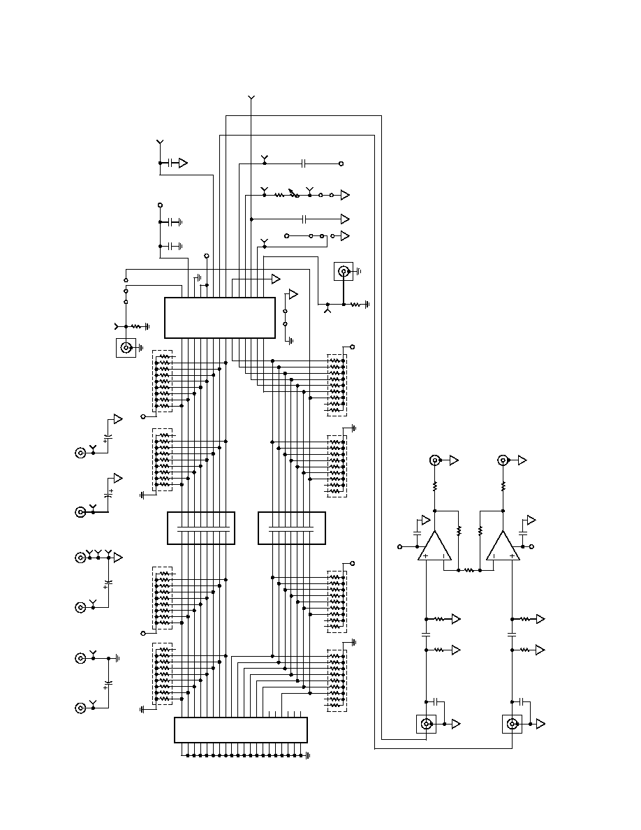
1
0
98
76
54
32
1
R4
10
9
8
7
6
5
4
3
2
1
R7
DVDD
10
9
8
7
6
5
4
3
2
1
R3
1
0
98
76
54
32
1
DVDD
R6
2
4
6
8
10
12
14
16
18
20
22
24
26
28
30
32
34
36
38
40
1
3
5
7
9
11
13
15
17
19
21
23
25
27
29
31
33
35
37
39
P1
10
9
8
7
6
5
4
3
2
1
R5
DVDD
10
9
8
7
6
5
4
3
2
1
R1
16
15
14
13
12
11
10
9
1
2
3
4
5
6
7
8
C19
C1
C2
C25
C26
C27
C28
C29
16 PINDIP
RES PK
16
15
14
13
12
11
10
1
2
3
4
5
6
7
C30
C31
C32
C33
C34
C35
C36
16 PINDIP
RES PK
1
2
3
4
5
6
7
8
9
10
11
12
13
14
28
27
26
25
24
23
22
21
20
19
18
17
16
15
DB13
DB12
DB11
DB10
DB9
DB8
DB7
DB6
DB5
DB4
DB3
DB2
DB1
DB0
CLOCK
DVDD
DCOM
NC
AVDD
COMP2
I
OUTA
ACOM
COMP1
FS ADJ
REFIO
REFLO
SLEEP
U1
AD9754
I
OUTB
AVDD
CT1
A
1
A
R15
49.9
CLK
JP1
AB
3
2
1
J1
TP1
EXTCLK
C7
1
F
C8
0.1
F
AVDD
A
C9
0.1
F
TP8
2
AVDD
TP11
C11
0.1
F
TP10
TP9
R16
2k
TP14
JP4
C10
0.1
F
OUT 1
OUT 2
TP13
R17
49.9
PDIN
J2
A
A
A
AVDD
3
JP2
TP12
TP7
A
C6
10
F
AVCC
B6
TP6
A
C5
10
F
AVEE
B5
TP19
A
AGND
B4
TP18
TP5
C4
10
F
TP4
AVDD
B3
TP2
DGND
B2
C3
10
F
TP3
DVDD
B1
J3
C12
22pF
A
J4
C13
22pF
98
76
54
32
1
R2
10
1
0
98
76
54
32
1
DVDD
R8
OUT2
OUT1
A
R
20k
49.9
A
49.9
A
10k
A
10k
A
1
F
1
F
AD8002
A
AVCC
249
A
0.1
F
AD8002
A
AVEE
A
0.1
F
226
750
750
249
DIFFERENTIAL
DMT OUTPUTS
TO TEK
AWG
2021
Figure 37. DMT Signal Generator Schematic
AD8022
13
REV. 0
AD8022
AD8022
U27
U27
12V
1k
1%
1k
1%
1
8
3
2
7
4
6
5
1.69k
1%
0.1 F
50V
5%
NPO
820pF
10%
820pF
10%
680pF
5% NPO
2.43k
1%
1.91k
1%
6V
0.1 F
16V
10%
X7R
2.43k
1%
1.91k
1%
680pF
5% NPO
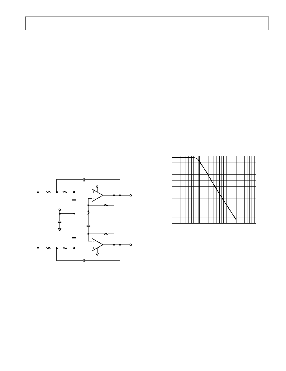
Figure 38. Differential Input Sallen-Key Filter Using
AD8022 on Single Supply, 12 V
EVALUATION BOARDS
The evaluation board layout of Figures 40, 41, and 42 is our
standard dual SOIC noninverting evaluation circuit offering
the ability to evaluate the AD8022 in typical op amp circuits,
is available from Analog Devices Inc. In addition, the AD8022
receiver function may be added to on our ADSL EVAL boards.
The AD8016ARB-EVAL, the AD8016ARP-EVAL, the
AD8017AR-EVAL and AD8018ARU-EVAL boards are avail-
able through Analog Devices. These platforms provide the
capability to fully evaluate the Analog Devices ADSL trans-
ceiver hybrid. All of the ADSL evaluation boards mentioned
above can accommodate the evaluation of the AD8022 as a
receiver amplifier when installed in the U2 location. The receiver
circuit on these boards is typically unpopulated. Requesting
samples of the AD8022 along with the EVAL board of your
choice will provide the capability to evaluate the AD8022 along
with many other Analog Devices ADSL line driver products in a
typical transceiver circuit. The evaluation circuits have been
designed to replicate the CPE or CO side analog transceiver
hybrid circuits.
The ADSL EVAL circuits mentioned above are designed using a
two transformer transceiver topology, including a line receiver, line
driver, line matching network, an RJ11 jack for interfacing to
line simulators, and transformer-coupled inputs for single-to-
differential input conversion.
Layout Considerations
As is the case with all "hi speed" amplifiers, careful attention to
printed circuit board layout details will prevent associated board
parasitics from becoming problematic. Proper RF design technique
is mandatory. The PCB should have a ground plane covering all
unused portions of the component side of the board to provide a
low-impedance return path. Removing the ground plane from
the area near the input signal lines will reduce stray capacitance.
Chip capacitors should be used for the supply bypassing. One
end of the capacitor connected to the ground plane and the other
no more than 1/8 inch away from each supply pin. An additional
large (0.47
µ
F to 10
µ
F) tantalum capacitor should be connected
in parallel, although not necessarily as close, in order to supply
current for fast, large signal changes at the AD8022 output.
Signal lines connecting the feedback and gain resistors should
be as short as possible, minimizing the inductance and stray
capacitance associated with these traces. Locate termination
resistors and loads as close as possible to the input(s) and out-
put respectively. Adhere to stripline design techniques for long
signal traces (greater than about 1 inch). Following these
generic guidelines will improve the performance of the AD8022
in all applications.
FREQUENCY Hz
10k
47.5
100k
1M
10M
42.5
37.5
32.5
27.5
22.5
17.5
12.5
7.5
2.5
2.5
7.5
dB
Figure 39. Frequency Response of Sallen-Key Filter
AD8022
14
REV. 0
Figure 40.
Figure 41.
Figure 42.
+V
S
C3
0.01 F
C4
0.01 F
C1
10 F
C2
10 F
V
S
BYPASSING
AD8022
R
G
715
R
F
715
R
C
0
R
O
0
49.9
J3
J4
499
AMP #2
G = 2
AD8022
R
G
715
R
F
715
R
C
0
R
O
0
R
T
49.9
J1
J2
499
AMP #1
G = 2
+V
S
V
S
Figure 43. Evaluation Board Schematic
AD8022
15
REV. 0
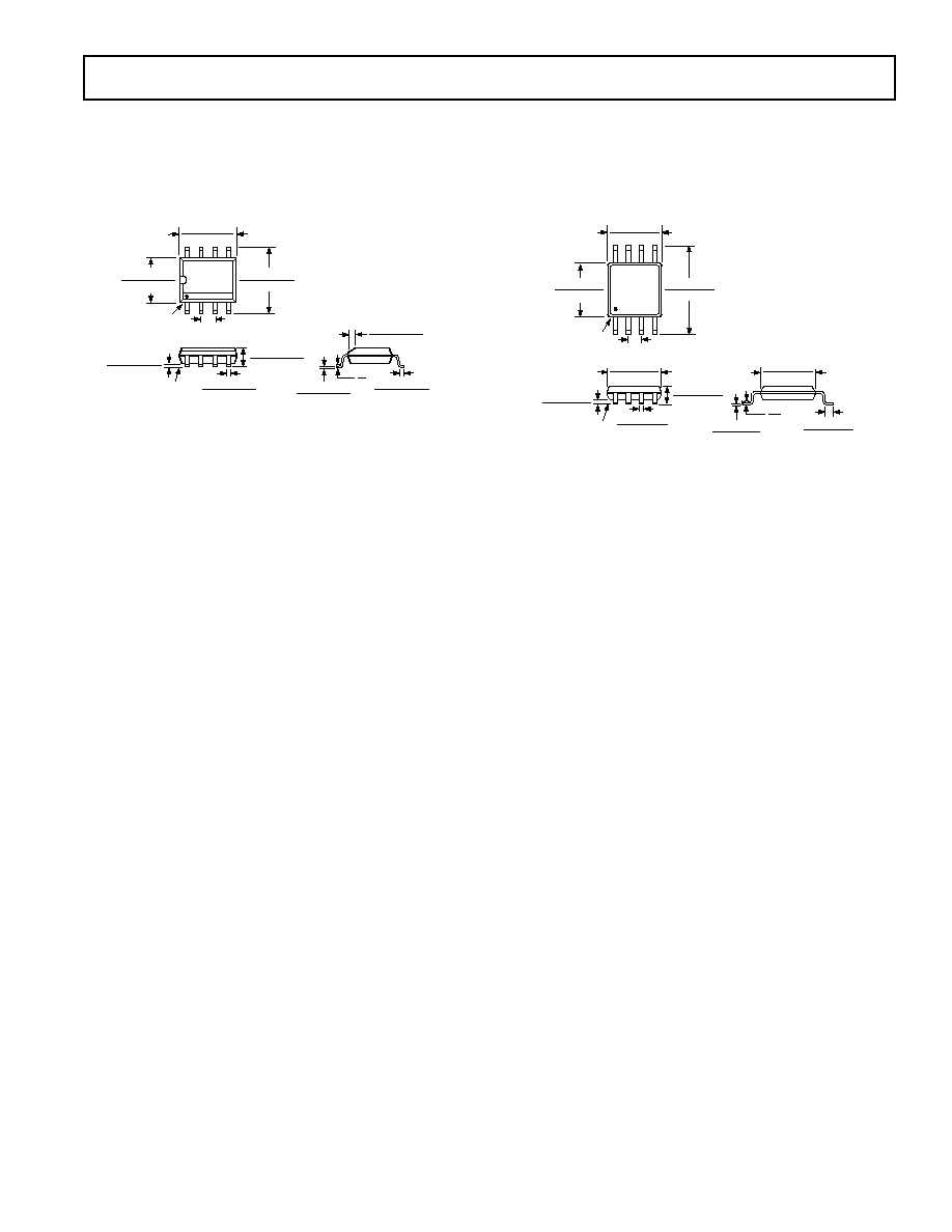
OUTLINE DIMENSIONS
Dimensions shown in inches and (mm).
8-Lead Plastic SOIC
(SO-8)
0.0098 (0.25)
0.0075 (0.19)
0.0500 (1.27)
0.0160 (0.41)
8
0
0.0196 (0.50)
0.0099 (0.25)
45
8
5
4
1
0.1968 (5.00)
0.1890 (4.80)
0.2440 (6.20)
0.2284 (5.80)
PIN 1
0.1574 (4.00)
0.1497 (3.80)
0.0500 (1.27)
BSC
0.0688 (1.75)
0.0532 (1.35)
SEATING
PLANE
0.0098 (0.25)
0.0040 (0.10)
0.0192 (0.49)
0.0138 (0.35)
8-Lead microSOIC
(RM-8)
0.011 (0.28)
0.003 (0.08)
0.028 (0.71)
0.016 (0.41)
33
27
0.120 (3.05)
0.112 (2.84)
8
5
4
1
0.122 (3.10)
0.114 (2.90)
0.199 (5.05)
0.187 (4.75)
PIN 1
0.0256 (0.65) BSC
0.122 (3.10)
0.114 (2.90)
SEATING
PLANE
0.006 (0.15)
0.002 (0.05)
0.018 (0.46)
0.008 (0.20)
0.043 (1.09)
0.037 (0.94)
0.120 (3.05)
0.112 (2.84)
C3714810/99
PRINTED IN U.S.A.