 | ÐлекÑÑоннÑй компоненÑ: AD8026 | СкаÑаÑÑ:  PDF PDF  ZIP ZIP |
Äîêóìåíòàöèÿ è îïèñàíèÿ www.docs.chipfind.ru
REV. 0
Information furnished by Analog Devices is believed to be accurate and
reliable. However, no responsibility is assumed by Analog Devices for its
use, nor for any infringements of patents or other rights of third parties
which may result from its use. No license is granted by implication or
otherwise under any patent or patent rights of Analog Devices.
a
AD8026
One Technology Way, P.O. Box 9106, Norwood, MA 02062-9106, U.S.A.
Tel: 781/329-4700
World Wide Web Site: http://www.analog.com
Fax: 781/326-8703
© Analog Devices, Inc., 1998
Quad High Speed
Amplifier
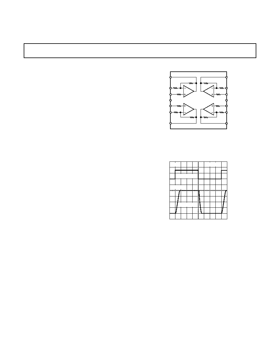
FUNCTIONAL BLOCK DIAGRAM
R
F
R
G
R
G
R
F
V
EE
V
CC
AD8026
R
F
R
P
R
P
OUT A
IN A
+IN A
+IN B
IN B
OUT B
OUT D
IN D
+IN D
+IN C
IN C
OUT C
R
F
R
G
R
P
R
P
R
G
PRODUCT DESCRIPTION
The AD8026 is a complete low cost, closed loop, voltage feed-
back, quad amplifier. Precision trimmed resistors set a fixed R
F
/
R
G
ratio of 5/3 to a typical gain accuracy of 0.02%. Manufac-
tured on ADI's proprietary XFCB high speed bipolar process,
which enables the output drivers to settle to within 0.1% within
55 ns into a 100 pF load (4 V swing) and drive output voltages
to rated settling time to within 0.5 V from the rail. The typical
3 dB bandwidth is 60 MHz, at G = +2.67. The AD8026 is
laser trimmed to produce both exceptional offset and gain
performance.
The low settling time, high slew rate, low offset and rail-to-rail
output voltage drive capability makes the AD8026 ideal for
driving LCD displays.
The AD8026 is available in a 14-lead SOIC package.
FEATURES
Voltage Feedback, Rail-to-Rail Output
Rated Settling Time to Within 0.5 V of Supply Rail
Quad High Speed Amplifier
Settling Time to 0.1% of 55 ns (4 V Swing, C
L
= 100 pF)
Slew Rate 135 V/ s (4 V Swing)
3 dB Bandwidth 60 MHz
Fixed Gain Resistors for High DC Accuracy
Low Voltage Offset 0.5 mV RTO Typical
Gain Error Less than 0.05%
Low Supply Current 3.4 mA
Nominal +12 V Supply
14-Lead SOIC Package
APPLICATIONS
LCD Source Drivers
CD DVD
CDR
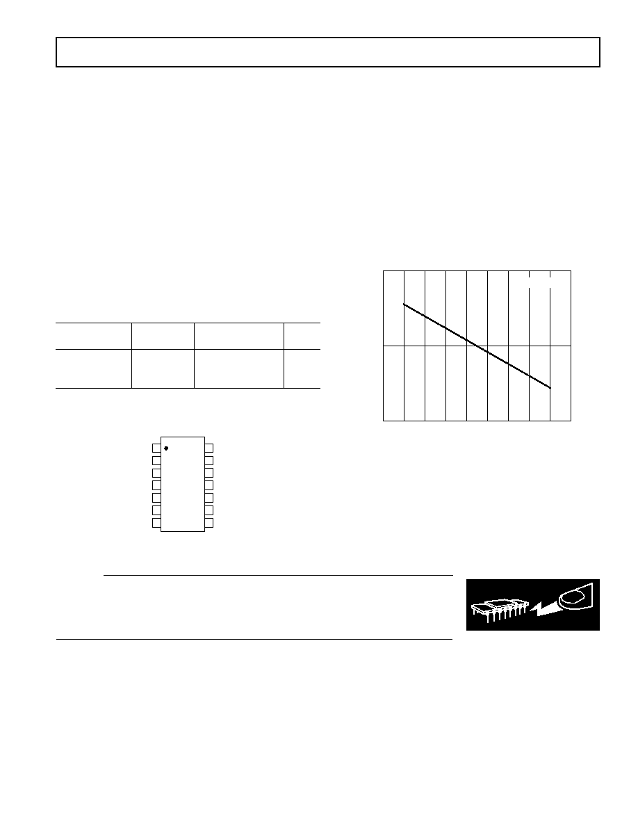
1V/DIV
1V/DIV
50ns/DIV
INPUT
OUTPUT
V
OUT
= 4V
V
IN
= 1.5V
R
L
= 10k
Figure 1. 4 V Step Response

2
REV. 0
AD8026SPECIFICATIONS
Parameter
Conditions
Min
Typ
Max
Units
DYNAMIC PERFORMANCE
3 dB Small Signal Bandwidth
V
IN
= 50 mV rms
R
L
= 1 k
20
60
MHz
Bandwidth for 0.1 dB Flatness
V
IN
= 50 mV rms
R
L
= 1 k
12
MHz
Slew Rate
V
O
= 4 V Step
135
V/
µ
s
Full Power Response
V
O
= 2 V p-p
10
MHz
Settling Time to 0.1%
V
O
= 4 V Step, C
L
= 100 pF,
R
S
= 50
55
ns
NOISE/DISTORTION PERFORMANCE
Total Harmonic Distortion
f
C
= 5 MHz, V
O
= 2 V p-p,
R
L
= 1 k
60
dBc
Voltage Noise (RTO)
1
f = 10 kHz
67
nV/
Hz
Crosstalk, Output to Output
f = 5 MHz, V
O
= 2 V p-p,
R
L
= 1 k
80
dB
Differential Gain Error
NTSC R
L
= 1 k
0.02
%
Differential Phase Error
NTSC R
L
= 1 k
0.02
Degrees
DC PERFORMANCE
RTO Offset Voltage
2
V
IN
= 0 V
0.5
5.5
mV
T
MIN
to T
MAX
6
mV
RTO Offset Drift
10
µ
V/
°
C
+Input Bias Current
0.6
1.6
µ
A
Closed-Loop Gain Error
3
R
L
= 10 k
, 2.67 < V
O
< +2.67
0.02
0.05
%
T
MIN
to T
MAX
0.05
%
Gain Matching
Channel-to-Channel, R
L
= 10 k
0.03
%
INPUT CHARACTERISTICS
+Input Resistance
170
k
+Input Capacitance
2.5
pF
OUTPUT CHARACTERISTICS
Output Voltage Swing
R
L
= 10 k
, V
CC
V
OH
, V
EE
+ V
OL
0.2
0.25
V
Short Circuit Output Current
175
mA
POWER SUPPLY
Operating Range
4
13
V
Quiescent Current/Amp
3.2
3.4
mA/Amp
Power Supply Rejection Ratio (RTO)
+V
S
= 5.5 V to 6.5 V, V
S
= 6 V
48
60
dB
V
S
= 5.5 V to 6.5 V, +V
S
= 6 V
48
65
dB
OPERATING TEMPERATURE RANGE
0
+70
°
C
NOTES
1
Includes gain resistor thermal noise.
2
RTO offset includes effects of input voltage offset, input current, and input offset current.
3
Measured in the inverting mode.
4
Observe Absolute Maximum Ratings.
Specifications subject to change without notice.
(@ +25 C, V
S
= 6 V, R
I
= 500
, R
L
= 10 k
, R
F
= 5K, R
G
= 3K Noninverting
Configuration, T
MIN
= 0 C, T
MAX
= +70 C, unless otherwise noted.)
AD8026
3
REV. 0
ABSOLUTE MAXIMUM RATINGS
1
Supply Voltage V
CC
V
EE
. . . . . . . . . . . . . . . . . . . . . . . 14.0 V
Internal Power Dissipation
2
Small Outline Package (R) . . . . . . . . . . . . . . . . . . . . 0.9 W
+Input Voltage V
CC
V
IN
+ . . . . . . . . . . . . . . . . . . . . . . < 12 V
Input Voltage . . . . . . . . . . . . . . . . . . . . . . . . . . < V
EE
+ 12 V
. . . . . . . . . . . . . . . . . . . . . . . . . . . . . . . . . . . . . > V
EE
12 V
Output Short Circuit Duration
. . . . . . . . . . . . . . . . . . . . Observe Power Derating Curves
Storage Temperature Range . . . . . . . . . . . . 65
°
C to +125
°
C
Operating Temperature Range (A Grade) . . . . 0
°
C to +70
°
C
Lead Temperature Range (Soldering 10 sec) . . . . . . . +300
°
C
NOTES
1
Stresses above those listed under Absolute Maximum Ratings may cause perma-
nent damage to the device. This is a stress rating only; functional operation of the
device at these or any other conditions above those indicated in the operational
section of this specification is not implied. Exposure to absolute maximum rating
conditions for extended periods may affect device reliability.
2
Specification is for device in free air:
14-Lead SOIC Package:
JA
= 120
°
C/W, where P
D
= (T
J
T
A
)/
JA
.
MAXIMUM POWER DISSIPATION
The maximum power that can be safely dissipated by the
AD8026 is limited by the associated rise in junction tempera-
ture. The maximum safe junction temperature for plastic
encapsulated devices is determined by the glass transition tem-
perature of the plastic, approximately +150
°
C. Exceeding this
limit temporarily may cause a shift in parametric performance
due to a change in the stresses exerted on the die by the package.
Exceeding a junction temperature of +175
°
C for an extended
period can result in device failure.
While the AD8026 is internally short circuit protected, this
may not be sufficient to guarantee that the maximum junction
temperature (+150
°
C) is not exceeded under all conditions. To
ensure proper operation, it is necessary to observe the maximum
power derating curves.
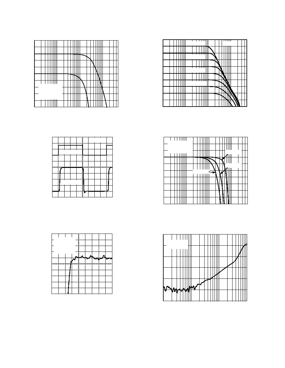
AMBIENT TEMPERATURE C
1.5
1.0
0.5
10
80
0
MAXIMUM POWER DISSIPATION Watts
10
20
30
40
50
60
70
T
J
= +150 C
Figure 2. Maximum Power Dissipation vs. Temperature
ORDERING GUIDE
Temperature
Package
Package
Model
Range
Description
Option
AD8026AR
0
°
C to +70
°
C
14-Lead Plastic SOIC SO-14
AD8026AR-REEL
0
°
C to +70
°
C
REEL SOIC
SO-14
AD8026AR-REEL7 0
°
C to +70
°
C
REEL 7 SOIC
SO-14
CAUTION
ESD (electrostatic discharge) sensitive device. Electrostatic charges as high as 4000 V readily
accumulate on the human body and test equipment and can discharge without detection.
Although the AD8026 features proprietary ESD protection circuitry, permanent damage may
occur on devices subjected to high energy electrostatic discharges. Therefore, proper ESD
precautions are recommended to avoid performance degradation or loss of functionality.
WARNING!
ESD SENSITIVE DEVICE
PIN CONFIGURATION
TOP VIEW
(Not to Scale)
14
13
12
11
10
9
8
1
2
3
4
5
6
7
IN A
+IN A
V
CC
+IN B
IN B
OUT B
OUT D
IN D
+IN D
V
EE
+IN C
OUT A
AD8026
IN C
OUT C
AD8026Typical Performance Characteristics
4
REV. 0
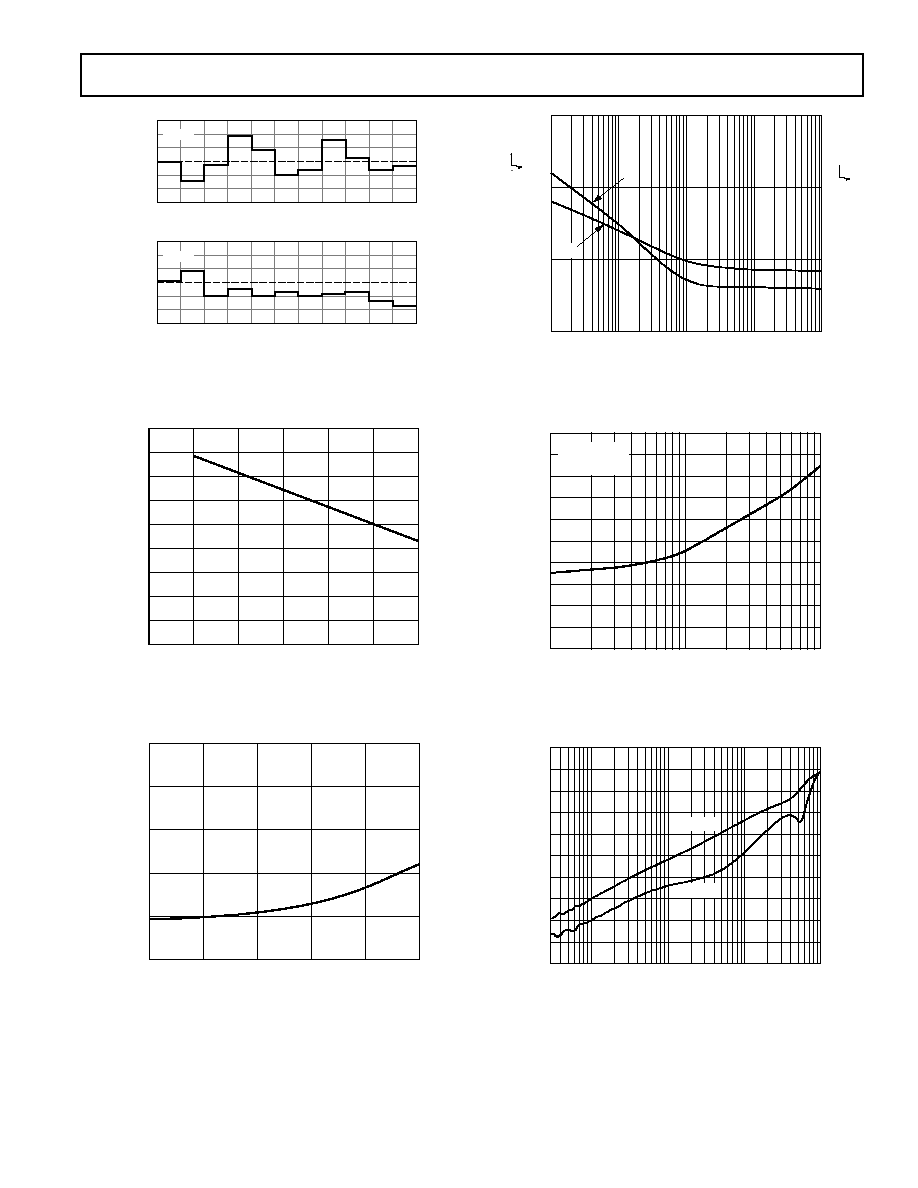
FREQUENCY Hz
0.5
0.4
0.5
0.1
0.2
0.3
0.4
0.3
0.2
0.1
0
100k
500M
1M
10M
100M
NORMALIZED FLATNESS dB
8
NORMALIZED OUTPUT dB
2
1
0
1
2
3
4
5
6
7
V
IN
= 50mV rms
R
L
= 1k
R
S
= 0
C
L
= 0pF
Figure 3. Small Signal Bandwidth and 0.1 dB Flatness
20mV/DIV
25mV/DIV
50ns/DIV
V
OUT
= 100mV
V
IN
= 37.5mV
R
L
= 10k
Figure 4. 100 mV Step Response
0.1%
/
DIV
TIME ns
0
20
40
60
80
100 120 140 160 180
V
IN
= 4V STEP
R
L
= 10k
R
S
= 50
C
L
= 100pF
Figure 5. Short-Term Settling Time
FREQUENCY Hz
100k
500M
1M
10M
100M
OUTPUT dBm
V
IN
= 2.0V p-p
R
L
= 1k
8.5
5.5
2.5
0.5
3.5
6.5
9.5
12.5
15.5
18.5
21.5
V
IN
= 1.0V p-p
V
IN
= 0.5V p-p
V
IN
= 0.25V p-p
Figure 6. Large Signal Bandwidth
FREQUENCY Hz
100k
500M
1M
10M
100M
C
L
= 100pF
C
L
= 200pF
C
L
= 300pF
V
IN
= 50mV rms
R
L
= 1k
R
S
= 25
NORMALIZED OUTPUT dB
3
2
1
0
1
2
3
4
5
6
7
Figure 7. Cap Load vs. Frequency
FREQUENCY Hz
0
20
120
100k
100M
1M
10M
40
60
80
100
V
OUT
= 2V p-p
R
L
= 1k
CROSSTALK dB
Figure 8. Crosstalk (Output-to-Output) vs. Frequency
AD8026
5
REV. 0
IRE
1
2
3
4
5
6
7
8
9
10
11
DIFF PHASE Degrees
NTSC
0.02
0.01
0.00
0.02
0.01
0.03
0.03
DIFF GAIN %
NTSC
IRE
1
2
3
4
5
6
7
8
9
10
11
0.02
0.01
0.00
0.02
0.01
0.03
0.03
Figure 9. Differential Gain and Differential Phase
0
0.2
1.8
V
OS
RTO mV 1.0
1.2
1.4
1.6
0.6
0.8
0.4
TEMPERATURE C
15
25
40
55
70
0
15
Figure 10. V
OS
RTO vs. Temperature
0
0.0005
0.0025
GAIN ACCURACY %
0.0015
0.002
0.001
TEMPERATURE C
15
25
40
55
70
0
Figure 11. Gain Accuracy vs. Temperature
10
100
NOISE VOLTAGE, RTO nV/
Hz
NOISE CURRENT pA
/
Hz
FREQUENCY Hz
10000
10k
100k
1000
100
10
1k
100
10
1
0.1
en
in
Figure 12. Noise (RTO) vs. Frequency
FREQUENCY Hz
30
90
130
1M
10M
DISTORTION dBc
100
110
120
100k
40
50
60
70
80
R
L
= 1k
V
OUT
= 2V p-p
Figure 13. Total Harmonic Distortion
FREQUENCY Hz
20
10
80
30k
100M
100k
1M
10M
20
50
60
70
0
10
40
30
POWER SUPPLY REJECTION RATIO dB
PSRR
+PSRR
Figure 14. PSRR vs. Frequency