 | –≠–Ľ–Ķ–ļ—ā—Ä–ĺ–Ĺ–Ĺ—č–Ļ –ļ–ĺ–ľ–Ņ–ĺ–Ĺ–Ķ–Ĺ—ā: AD8027 | –°–ļ–į—á–į—ā—Ć:  PDF PDF  ZIP ZIP |
Low Distortion, High Speed
Rail-to-Rail Input/Output Amplifiers
AD8027/AD8028
FEATURES
High speed
190 MHz, ≠3 dB bandwidth (G = +1)
100 V/Ķs slew rate
Low distortion
120 dBc @ 1 MHz SFDR
80 dBc @ 5 MHz SFDR
Selectable input crossover threshold
Low noise
4.3 nV/Hz
1.6 pA/Hz
Low offset voltage: 900 ĶV max
Low power: 6.5 mA/amplifier supply current
Power-down mode
No phase reversal: V
IN
> |V
S
| + 200 mV
Wide supply range: 2.7 V to 12 V
Small packaging: SOIC-8, SOT-23-6, MSOP-10
APPLICATIONS
Filters
ADC drivers
Level shifting
Buffering
Professional video
Low voltage instrumentation
GENERAL DESCRIPTION
The AD8027/AD8028
1
is a high speed amplifier with rail-to-
rail input and output that operates on low supply voltages and
is optimized for high performance and wide dynamic signal
range. The AD8027/AD8028 has low noise (4.3 nV/Hz,
1.6 pA/Hz) and low distortion (120 dBc @ 1 MHz). In appli-
cations that use a fraction of or the entire input dynamic range
and require low distortion, the AD8027/AD8028 is an ideal
choice.
Many rail-to-rail input amplifiers have an input stage that
switches from one differential pair to another as the input sig-
nal crosses a threshold voltage, which causes distortion. The
AD8027/AD8028 has a unique feature that allows the user to
select the input crossover threshold voltage through the
SELECT pin. This feature controls the voltage at which the
complementary transistor input pairs switch. The AD8027/
AD8028 also has intrinsically low crossover distortion.
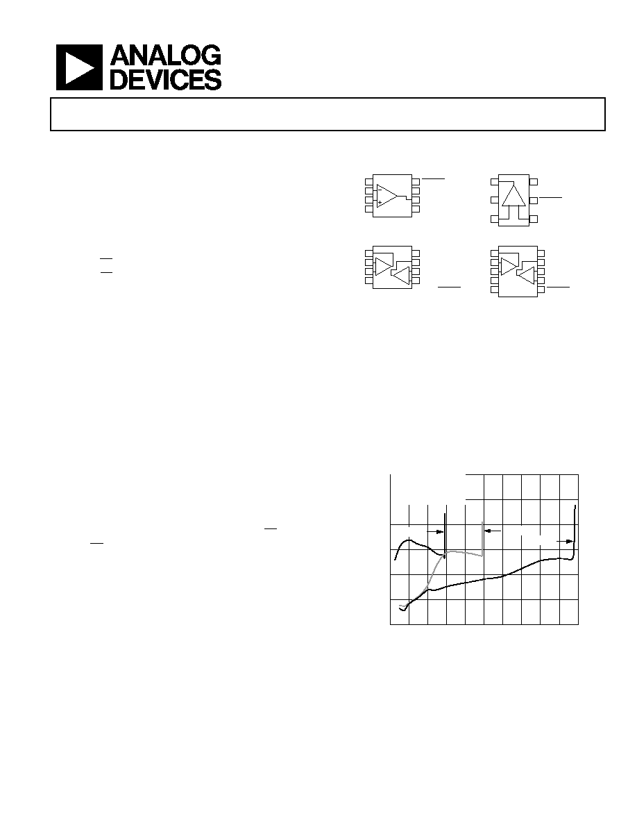
CONNECTION DIAGRAMS
SOT-23-6
(RT)
V
OUT
1
≠V
S
2
+IN
3
5
6
+V
S
DISABLE/SELECT
4
≠IN
+
≠
03327-B-001
NC = NO CONNECT
NC
SOIC-8
(R)
1
≠IN
2
+IN
3
≠V
S
4
+V
S
V
OUT
NC
8
7
6
5
DISABLE/SELECT
V
OUTB
≠IN B
+IN B
8
7
6
5
+V
S
V
OUTA
SOIC-8
(R)
1
≠IN A
2
+IN A
3
≠V
S
4
+
≠
+
≠
V
OUTB
10
9
+V
S
DISABLE/SELECT B
≠IN B
+IN B
8
7
6
DISABLE/SELECT A
V
OUTA
MSOP-10
(RM)
1
≠IN A
2
+IN A
3
≠V
S
4
5
+
≠
+
≠
Figure 1. Connection Diagrams (Top View)
With its wide supply voltage range (2.7 V to 12 V) and wide
bandwidth (190 MHz), the AD8027/AD8028 amplifier is
designed to work in a variety of applications where speed and
performance are needed on low supply voltages. The high per-
formance of the AD8027/AD8028 is achieved with a quiescent
current of only 6.5 mA/amplifier typical. The AD8027/AD8028
has a shut down mode that is controlled via the SELECT pin.
The AD8027/AD8028 is available in SOIC-8, MSOP-10, and
SOT-23-6 packages. They are rated to work over the industrial
temperature range of ≠40įC to +125įC.
OUTPUT VOLTAGE (V p-p)
0
1
2
3
4
5
6
7
8
9
10
≠140
≠120
≠100
≠80
≠60
≠40
≠20
SF
DR (d
B)
G = +1
FREQUENCY = 100kHz
R
L
= 1k
V
S
=
Ī5V
V
S
= +3V
V
S
= +5V
03327-A-063
Figure 2. SFDR vs. Output Amplitude
1
Protected by U.S. patent numbers 6,486,737B1; 6,518,842B1
Rev. B
Information furnished by Analog Devices is believed to be accurate and reliable.
However, no responsibility is assumed by Analog Devices for its use, nor for any
infringements of patents or other rights of third parties that may result from its use.
Specifications subject to change without notice. No license is granted by implication
or otherwise under any patent or patent rights of Analog Devices. Trademarks and
registered trademarks are the property of their respective owners.
One Technology Way, P.O. Box 9106, Norwood, MA 02062-9106, U.S.A.
Tel: 781.329.4700
www.analog.com
Fax: 781.326.8703
© 2003 Analog Devices, Inc. All rights reserved.

AD8027/AD8028
Rev. B | Page 2 of 24
TABLE OF CONTENTS
Specifications..................................................................................... 3
Absolute Maximum Ratings............................................................ 6
Maximum Power Dissipation ..................................................... 6
Typical Performance Characteristics ............................................. 7
Theory of Operation ...................................................................... 16
Input Stage................................................................................... 16
Crossover Selection .................................................................... 16
Output Stage................................................................................ 17
DC Errors .................................................................................... 17
Wideband Operation ..................................................................... 18
Circuit Considerations .............................................................. 19
Applications..................................................................................... 20
Using the AD8027/AD8028 SELECT Pin ............................... 20
Driving a 16-Bit ADC ................................................................ 20
Band-Pass Filter.......................................................................... 21
Design Tools and Technical Support ....................................... 21
Outline Dimensions ....................................................................... 22
Ordering Guide .......................................................................... 23
REVISION HISTORY
Revision B:
10/03--Data Sheet changed from Rev. A to Rev. B
Changes to Figure 1...........................................................................1
Revision A:
8/03--Data Sheet changed from Rev. 0 to Rev. A
Addition of AD8028........................................................... Universal
Changes to GENERAL DESCRIPTION.........................................1
Changes to Figures 1, 3, 4, 8, 13, 15, 17............................ 1, 6, 7, 8, 9
Changes to Figures 58, 60 .........................................................18, 20
Changes to SPECIFICATIONS........................................................3
Updated OUTLINE DIMENSIONS .............................................22
Updated ORDERING GUIDE.......................................................23
Revision 0: Initial Version

AD8027/AD8028
Rev. B | Page 3 of 24
SPECIFICATIONS
Table 1. V
S
= Ī5 V (@ T
A
= 25įC, R
L
= 1 k to midsupply, G = +1, unless otherwise noted.)
Parameter Conditions Min
Typ
Max
Unit
DYNAMIC PERFORMANCE
G = +1, V
O
= 0.2 V p-p
138
190
MHz
≠3 dB Bandwidth
G = +1, V
O
= 2 V p-p
20
32
MHz
Bandwidth for 0.1 dB Flatness
G = +2, V
O
= 0.2 V p-p
16
MHz
Slew Rate
G = +1, V
O
= 2 V Step/G = ≠1, V
O
= 2 V Step
90/100
V/Ķs
Settling Time to 0.1%
G = +2, V
O
= 2 V Step
35
ns
NOISE/DISTORTION PERFORMANCE
f
C
= 1 MHz, V
O
= 2 V p-p, R
F
= 24.9
120
dBc
Spurious Free Dynamic Range (SFDR)
f
C
= 5 MHz, V
O
= 2 V p-p, R
F
= 24.9
80
dBc
Input Voltage Noise
f = 100 kHz
4.3
nV/
Hz
Input Current Noise
f = 100 kHz
1.6
pA/
Hz
Differential Gain Error
NTSC, G = +2, R
L
= 150
0.1
%
Differential Phase Error
NTSC, G = +2, R
L
= 150
0.2
Degree
Crosstalk, Output to Output
G = +1, R
L
=100 , V
OUT
= 2 V p-p,
V
S
= Ī5 V @ 1 MHz
≠93 dB
DC PERFORMANCE
Input Offset Voltage
SELECT = Tri-State or Open, PNP Active
200
800
ĶV
SELECT = High NPN Active
240 900
ĶV
Input Offset Voltage Drift
T
MIN
to T
MAX
1.50
ĶV/įC
V
CM
= 0 V, NPN Active
4
6
ĶA
Input Bias Current
1
T
MIN
to T
MAX
4
ĶA
V
CM
= 0 V, PNP Active
≠8
≠11
ĶA
Input Bias Current
1
T
MIN
to T
MAX
≠8
ĶA
Input Offset Current
Ī0.1
Ī0.9
ĶA
Open-Loop Gain
V
O
= Ī2.5 V
100
110
dB
INPUT CHARACTERISTICS
Input Impedance
6
M
Input Capacitance
2
pF
Input Common-Mode Voltage Range
≠5.2 to +5.2
V
Common-Mode Rejection Ratio
V
CM
= Ī2.5 V
90
110
dB
SELECT PIN
Crossover Low--Selection Input Voltage
≠3.3 to +5
V
Crossover High--Selection Input Voltage
≠3.9 to ≠3.3
V
Disable Input Voltage
Tri-State < Ī20 ĶA
≠5 to ≠3.9
V
Disable Switching Speed
980 ns
Enable Switching Speed
50% of Input to <10% of Final V
O
45 ns
OUTPUT CHARACTERISTICS
Output Overdrive Recovery Time
(Rising/Falling Edge)
V
I
= +6 V to ≠6 V, G = ≠1
40/45
ns
Output Voltage Swing
≠V
S
+ 0.10
+V
S
≠ 0.06,
≠V
S
+ 0.06
+V
S
≠ 0.10
V
Short Circuit Output
Sinking and Sourcing
120
mA
Off Isolation
V
IN
= 0.2 V p-p, f = 1 MHz, SELECT = Low
≠49
dB
Capacitive Load Drive
30% Overshoot
20
pF
POWER SUPPLY
Operating Range
2.7
12
V
Quiescent Current/Amplifier
6.5
8.5
mA
Quiescent Current (Disabled)
SELECT = Low
370
500
ĶA
Power Supply Rejection Ratio
V
S
Ī 1 V
90
110
dB
1
No sign or a plus indicates current into pin, minus indicates current out of pin.

AD8027/AD8028
Rev. B | Page 4 of 24
SPECIFICATIONS
Table 2. V
S
= +5 V (@ T
A
= 25įC, R
L
= 1 k to midsupply, unless otherwise noted.)
Parameter Conditions Min
Typ
Max
Unit
DYNAMIC PERFORMANCE
G = +1, V
O
= 0.2 V p-p
131
185
MHz
≠3 dB Bandwidth
G = +1, V
O
= 2 V p-p
18
28
MHz
Bandwidth for 0.1 dB Flatness
G = +2, V
O
= 0.2 V p-p
12
MHz
Slew Rate
G = +1, V
O
= 2 V Step/G = ≠1, V
O
= 2 V Step
85/100
V/Ķs
Settling Time to 0.1%
G = +2, V
O
= 2 V Step
40
ns
NOISE/DISTORTION PERFORMANCE
f
C
= 1 MHz, V
O
= 2 V p-p, R
F
= 24.9
90
dBc
Spurious Free Dynamic Range (SFDR)
f
C
= 5 MHz, V
O
= 2 V p-p, R
F
= 24.9
64
dBc
Input Voltage Noise
f = 100 kHz
4.3
nV/
Hz
Input Current Noise
f = 100 kHz
1.6
pA/
Hz
Differential Gain Error
NTSC, G = +2, R
L
= 150
0.1
%
Differential Phase Error
NTSC, G = +2, R
L
= 150
0.2
Degree
Crosstalk, Output to Output
G = 1, R
L
= 100 , V
OUT
= 2 V p-p,
V
S
= Ī5 V @ 1 MHz
≠92
dB
DC PERFORMANCE
Input Offset Voltage
SELECT = Tri-State or Open, PNP Active
200
800
ĶV
SELECT = High NPN Active
240 900
ĶV
Input Offset Voltage Drift
T
MIN
to T
MAX
2
ĶV/įC
V
CM
= 2.5 V, NPN Active
4
6
ĶA
Input Bias Current
1
T
MIN
to T
MAX
4
ĶA
V
CM
= 2.5 V, PNP Active
≠8
≠11
ĶA
Input Bias Current
1
T
MIN
to T
MAX
≠8
ĶA
Input Offset Current
Ī0.1
Ī0.9
ĶA
Open-Loop Gain
V
O
= 1 V to 4 V
96
105
dB
INPUT CHARACTERISTICS
Input Impedance
6
M
Input Capacitance
2
pF
Input Common-Mode Voltage Range
≠0.2 to +5.2
V
Common-Mode Rejection Ratio
V
CM
= 0 V to 2.5 V
90
105
dB
SELECT PIN
Crossover Low--Selection Input Voltage
1.7 to 5
V
Crossover High--Selection Input Voltage
1.1 to 1.7
V
Disable Input Voltage
0 to 1.1
V
DISABLE Switching Speed
1100
ns
Enable Switching Speed
Tri-State < Ī20 ĶA
50% of Input to <10% of Final V
O
50
ns
OUTPUT CHARACTERISTICS
Overdrive Recovery Time
(Rising/Falling Edge)
V
I
= ≠1 V to +6 V, G = ≠1
50/50
ns
Output Voltage Swing
R
L
= 1 k
≠V
S
+ 0.08
+V
S
≠ 0.04,
≠V
S
+ 0.04
+V
S
≠ 0.08 V
Off Isolation
V
IN
= 0.2 V p-p, f = 1 MHz, SELECT = Low
≠49
dB
Short Circuit Current
Sinking and Sourcing
105
mA
Capacitive Load Drive
30% Overshoot
20
pF
POWER SUPPLY
Operating Range
2.7
12
V
Quiescent Current/Amplifier
6
8.5
mA
Quiescent Current (Disabled)
SELECT = Low
320
450
ĶA
Power Supply Rejection Ratio
V
S
Ī 1 V
90
105
dB
1
No sign or a plus indicates current into pin, minus indicates current out of pin.

AD8027/AD8028
Rev. B | Page 5 of 24
SPECIFICATIONS
Table 3. V
S
= +3 V (@ T
A
= 25įC, R
L
= 1 k to midsupply, unless otherwise noted.)
Parameter Conditions
Min
Typ
Max
Unit
DYNAMIC PERFORMANCE
G = +1, V
O
= 0.2 V p-p
125
180
MHz
≠3 dB Bandwidth
G = +1, V
O
= 2 V p-p
19
29
MHz
Bandwidth for 0.1 dB Flatness
G = +2, V
O
= 0.2 V p-p
10
MHz
Slew Rate
G = +1, V
O
= 2 V Step/G = ≠1, V
O
= 2 V Step
73/100
V/Ķs
Settling Time to 0.1%
G = +2, V
O
= 2 V Step
48
ns
NOISE/DISTORTION PERFORMANCE
f
C
= 1 MHz, V
O
= 2 V p-p, R
F
= 24.9
85 dBc
Spurious Free Dynamic Range (SFDR)
f
C
= 5 MHz, V
O
= 2 V p-p, R
F
= 24.9
64 dBc
Input Voltage Noise
f = 100 kHz
4.3
nV/
Hz
Input Current Noise
f = 100 kHz
1.6
pA/
Hz
Differential Gain Error
NTSC, G = +2, R
L
= 150
0.15
%
Differential Phase Error
NTSC, G = +2, R
L
= 150
0.20
Degree
Crosstalk, Output to Output
G = 1, R
L
= 100 , V
OUT
= 2 V p-p,
V
S
= 3 V @ 1 MHz
≠89
dB
DC PERFORMANCE
SELECT = Tri-State or Open, PNP Active
200
800
ĶV
Input Offset Voltage
SELECT = High NPN Active
240
900
ĶV
Input Offset Voltage Drift
T
MIN
to T
MAX
2
ĶV/įC
V
CM
= 1.5 V, NPN Active
4
6
ĶA
Input Bias Current
1
T
MIN
to T
MAX
4
ĶA
V
CM
= 1.5 V, PNP Active
≠8
≠11
ĶA
Input Bias Current
1
T
MIN
to T
MAX
≠8
ĶA
Input Offset Current
Ī0.1
Ī0.9
ĶA
Open-Loop Gain
V
O
= 1 V to 2 V
90
100
dB
INPUT CHARACTERISTICS
Input Impedance
6
M
Input Capacitance
2
pF
Input Common-Mode Voltage Range
R
L
= 1 k
≠0.2 to +3.2
V
Common-Mode Rejection Ratio
V
CM
= 0 V to 1.5 V
88
100
dB
SELECT PIN
Crossover Low--Selection Input Voltage
1.7 to 3
V
Crossover High--Selection Input Voltage
1.1 to 1.7
V
Disable Input Voltage
0 to 1.1
V
DISABLE Switching Speed
1150
ns
Enable Switching Speed
Tri-State < Ī20 ĶA
50% of Input to <10% of Final V
O
50 ns
OUTPUT CHARACTERISTICS
Output Overdrive Recovery Time
(Rising/Falling Edge)
V
I
= ≠1 V to +4 V, G = ≠1
55/55
ns
Output Voltage Swing
R
L
= 1 k
≠V
S
+ 0.07
+V
S
≠ 0.03,
≠V
S
+ 0.03
+V
S
≠ 0.07
V
Short Circuit Current
Sinking and Sourcing
72
mA
Off Isolation
V
IN
= 0.2 V p-p, f = 1 MHz, SELECT = Low
≠49
dB
Capacitive Load Drive
30% Overshoot
20
pF
POWER SUPPLY
Operating Range
2.7
12
V
Quiescent Current/Amplifier
6.0
8.0
mA
Quiescent Current (Disabled)
SELECT = Low
300
420
ĶA
Power Supply Rejection Ratio
V
S
Ī 1 V
88
100
dB
1
No sign or a plus indicates current into pin, minus indicates current out of pin.

AD8027/AD8028
Rev. B | Page 6 of 24
ABSOLUTE MAXIMUM RATINGS
Table 4.
Parameter Rating
Supply Voltage
12.6 V
Power Dissipation
See Figure 3
Common-Mode Input Voltage
ĪV
S
Ī 0.5 V
Differential Input Voltage
Ī1.8 V
Storage Temperature
≠65įC to +125įC
Operating Temperature Range
≠40įC to +125įC
Lead Temperature Range
(Soldering 10 sec)
300įC
Junction Temperature
150įC
Stresses above those listed under Absolute Maximum Ratings
may cause permanent damage to the device. This is a stress rat-
ing only; functional operation of the device at these or any
other conditions above those indicated in the operational sec-
tion of this specification is not implied. Exposure to absolute
maximum rating conditions for extended periods may affect
device reliability.
Maximum Power Dissipation
The maximum safe power dissipation in the AD8027/AD8028
package is limited by the associated rise in junction temperature
(T
J
) on the die. The plastic encapsulating the die will locally
reach the junction temperature. At approximately 150įC, which
is the glass transition temperature, the plastic will change its
properties. Even temporarily exceeding this temperature limit
may change the stresses that the package exerts on the die,
permanently shifting the parametric performance of the
AD8027/AD8028. Exceeding a junction temperature of 175įC
for an extended period of time can result in changes in the
silicon devices, potentially causing failure.
The still-air thermal properties of the package and PCB (
JA
),
ambient temperature (T
A
), and the total power dissipated in the
package (P
D
) determine the junction temperature of the die.
The junction temperature can be calculated as
(
)
JA
D
A
J
P
T
T
◊
+
=
The power dissipated in the package (P
D
) is the sum of the
quiescent power dissipation and the power dissipated in the
package due to the load drive for all outputs. The quiescent
power is the voltage between the supply pins (V
S
) times the
quiescent current (I
S
). Assuming the load (R
L
) is referenced to
midsupply, then the total drive power is V
S
/2 ◊ I
OUT
, some of
which is dissipated in the package and some in the load (V
OUT
◊
I
OUT
). The difference between the total drive power and the load
power is the drive power dissipated in the package.
(
)
Power
Load
≠
Power
Drive
Total
Power
Quiescent
P
D
+
=
(
)
L
OUT
L
OUT
S
S
S
D
R
V
R
V
V
I
V
P
2
≠
2
◊
+
◊
=
RMS output voltages should be considered. If R
L
is referenced
to V
S≠
, as in single-supply operation, then the total drive power
is V
S
◊ I
OUT
.
If the rms signal levels are indeterminate, then consider the
worst case, when V
OUT
= V
S
/4 for R
L
to midsupply
(
) (
)
L
S
S
S
D
R
V
I
V
P
2
4
/
+
◊
=
In single-supply operation with R
L
referenced to V
S
≠, worst case
is V
OUT
= V
S
/2.
Airflow will increase heat dissipation, effectively reducing
JA
.
Also, more metal directly in contact with the package leads
from metal traces, through holes, ground, and power planes will
reduce the
JA
. Care must be taken to minimize parasitic capaci-
tances at the input leads of high speed op amps as discussed in
the board layout section.
Figure 3 shows the maximum safe power dissipation in the
package versus the ambient temperature for the SOIC-8
(125įC/W), SOT-23-6 (170įC/W), and MSOP-10 (130įC/W)
packages on a JEDEC standard 4-layer board.
OUTPUT SHORT CIRCUIT
Shorting the output to ground or drawing excessive current
from the AD8027/AD8028 will likely cause catastrophic failure.
AMBIENT TEMPERATURE (įC)
M
A
XIM
U
M
POW
E
R
D
I
SSIPA
TION
(
W
)
≠55
≠35
≠15
5
25
45
65
85
105
125
0
0.5
1.0
1.5
2.0
SOT-23-6
SOIC-8
MSOP-10
03327-A-002
Figure 3. Maximum Power Dissipation

AD8027/AD8028
Rev. B | Page 7 of 24
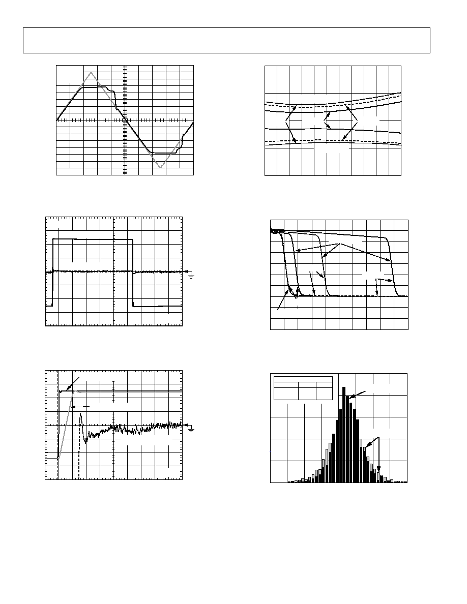
TYPICAL PERFORMANCE CHARACTERISTICS
Default Conditions V
S
= +5 V (T
A
= +25įC, R
L
= 1 k, unless otherwise noted.)
FREQUENCY (MHz)
0.1
1
10
100
1000
≠10
≠9
≠8
≠7
≠6
≠5
≠4
≠3
≠2
≠1
0
1
2
NORMALIZE
D
CLOS
E
D
-LOOP
GAIN (dB)
V
OUT
= 200mV p-p
03327-A-003
AD8027
G = +1
AD8028
G = +1
G = +10
G = ≠1
G = +2
Figure 4. Small Signal Frequency Response for Various Gains
FREQUENCY (MHz)
0.1
1
10
100
1000
≠10
≠9
≠8
≠7
≠6
≠5
≠4
≠3
≠2
≠1
0
1
2
CLOSED-
LOOP GAIN (
d
B)
G = +1
V
OUT
= 200mV p-p
V
S
= +5V
V
S
=
Ī5V
V
S
= +3V
V
S
= +3V R
F
= 24.9
03327-A-004
Figure 5. AD8027 Small Signal Frequency Response for Various Supplies
100
FREQUENCY (MHz)
0.1
1
10
1000
≠10
≠9
≠8
≠7
≠6
≠5
≠4
≠3
≠2
≠1
0
1
2
CLOSED-
L
OOP GAIN (
d
B)
G = +1
V
OUT
= 2V p-p
V
S
= +5V
V
S
=
Ī5V
V
S
= +3V
03327-A-005
Figure 6. Large Signal Frequency Response for Various Supplies
FREQUENCY (MHz)
0.1
1
10
100
1000
≠4
≠3
≠2
≠1
0
1
2
3
4
5
6
7
8
CLOSED-
L
OOP GAIN (
d
B)
G = +2
V
OUT
= 200mV p-p
V
S
= +5V
V
S
=
Ī5V
V
S
= +3V
03327-A-006
Figure 7. Small Signal Frequency Response for Various Supplies
FREQUENCY (MHz)
0.1
1
10
100
1000
≠10
≠9
≠8
≠7
≠6
≠5
≠4
≠3
≠2
≠1
0
1
2
CLOSED-
L
OOP GAIN (
d
B)
G = +1
V
OUT
= 200mV p-p
03327-A-007
V
S
= Ī5V
V
S
= +5V
V
S
= +3V
Figure 8. AD8028 Small Signal Frequency Response for Various Supplies
FREQUENCY (MHz)
0.1
1
10
100
1000
≠4
≠3
≠2
≠1
0
1
2
3
4
5
6
7
8
CLOSED-
L
OOP GAIN (
d
B)
G = +2
V
OUT
= 2V p-p
V
S
=
Ī5V
V
S
= +3V
V
S
= +5V
03327-A-008
Figure 9. Large Signal Frequency Response for Various Supplies

AD8027/AD8028
Rev. B | Page 8 of 24
FREQUENCY (MHz)
0.1
1
10
100
1000
CLOSED-
L
OOP GAIN (
d
B)
G = +1
V
OUT
= 200mV p-p
≠8
≠7
≠6
≠5
≠4
≠3
≠2
≠1
0
1
2
3
4
C
L
= 0pF
C
L
= 20pF
C
L
= 5pF
03327-A-009
Figure 10. AD8027 Small Signal Frequency Response for Various C
LOAD
FREQUENCY (MHz)
0.1
1
10
100
1000
≠4
≠3
≠2
≠1
0
1
2
3
4
5
6
7
8
CLOSED-
L
OOP GAIN (
d
B)
G = +2
V
OUT
= 200mV p-p
V
OUT
= 2V p-p
V
OUT
= 4V p-p
03327-A-010
Figure 11. Frequency Response for Various Output Amplitudes
FREQUENCY (MHz)
0.1
1
10
100
1000
≠8
≠7
≠6
≠5
≠4
≠3
≠2
≠1
1
0
2
CLOSED-
L
OOP GAIN (
d
B)
+125įC
≠40įC
+25įC
03327-A-011
G = +1
V
OUT
= 200mV p-p
Figure 12. AD8027 Small Signal Frequency Response vs. Temperature
FREQUENCY (MHz)
0.1
1
10
100
1000
≠10
≠9
≠8
≠7
≠6
≠5
≠4
≠3
≠2
≠1
0
1
3
2
CLOSED-
L
OOP GAIN (
d
B)
03327-A-012
C
L
= 0pF
C
L
= 20pF
C
L
= 5pF
G = +1
V
OUT
= 200mV p-p
Figure 13. AD8028 Small Signal Frequency Response for Various C
LOAD
FREQUENCY (MHz)
0.1
1
10
100
1000
≠4
≠3
≠2
≠1
0
1
2
3
5
4
6
7
8
CLOSED-
L
OOP GAIN (
d
B)
G = +2
V
OUT
= 0.2V p-p
R
L
= 1k
V
OUT
= 2.0V p-p
R
L
= 1k
V
OUT
= 2.0V p-p
R
L
= 150
V
OUT
= 0.2V p-p
R
L
= 150
03327-A-013
Figure 14. Small Signal Frequency Response for Various R
LOAD
Values
FREQUENCY (MHz)
0.1
1
10
100
1000
≠8
≠7
≠6
≠5
≠4
≠3
≠2
≠1
0
1
2
CLOSED-
L
OOP GAIN (
d
B)
G = +1
V
OUT
= 200mV p-p
03327-A-014
+25įC
≠40įC
+125įC
Figure 15. AD8028 Small Signal Frequency Response vs. Temperature
AD8027/AD8028
Rev. B | Page 9 of 24
FREQUENCY (MHz)
0.1
1
10
100
1000
CLOSED-
L
OOP GAI (
d
B)
G = +1
V
OUT
= 200mV p-p
≠8
≠7
≠6
≠5
≠4
≠3
≠2
≠1
0
1
2
3
4
V
ICM
= V
S+
≠ 0.2V
SELECT = HIGH
V
ICM
= 0V
SELECT = HIGH OR TRI
V
ICM
= V
S≠
+ 0.2V
SELECT = TRI
V
ICM
= V
S+
≠ 0.3V
SELECT = HIGH
V
ICM
= V
S≠
+ 0.3V
SELECT = TRI
03327-A-015
Figure 16. Small Signal Frequency Response vs.
Input Common-Mode Voltages
FREQUENCY (MHz)
0.001
0.01
0.1
1
10
100
1000
≠130
≠140
≠120
≠110
≠100
≠90
≠80
≠70
≠60
≠50
≠40
≠30
≠20
≠10
CROS
S
T
ALK (dB)
03327-A-016
G = +1
V
S
= 5V
R
L
= 1k
A TO B
B TO A
CROSSTALK = 20log (V
OUT
/V
IN
)
1/2
AD8028
+
U1
R3
1k
R2
50
R1
50
V1
VI
≠
1/2
AD8028
+
U2
V
OUT
≠
Figure 17. AD8028 Crosstalk Output to Output
FREQUENCY (Hz)
OPEN-
L
OOP GAIN (
d
B)
PH
A
SE (
D
egrees)
10
100
1k
10k
100k
1M
10M
100M
1G
≠25
≠5
15
35
55
75
95
115
135
≠10
0
10
20
30
40
50
60
70
80
90
100
110
GAIN
PHASE
03327-A-017
Figure 18. Open-Loop Gain and Phase vs. Frequency
1
10
100
1k
10k
100k
FREQUENCY (Hz)
1M
10M
100M
1G
10
100
CURRE
NT NOIS
E
(pA/ Hz)
1
10
100
VOLTA
GE N
O
ISE (
n
V/ H
z
)
VOLTAGE
CURRENT
03327-A-018
Figure 19. Voltage and Current Noise vs. Frequency
100
FREQUENCY (MHz)
0.1
1
10
1000
5.9
6.0
6.1
6.2
6.3
6.4
6.5
6.6
6.7
6.8
6.9
CLOSED-
L
OOP GAIN (
d
B)
G = +2
R
L
= 150
V
OUT
= 2V p-p
V
OUT
= 200mV p-p
03327-A-019
Figure 20. 0.1 dB Flatness Frequency Response
AD8027/AD8028
Rev. B | Page 10 of 24
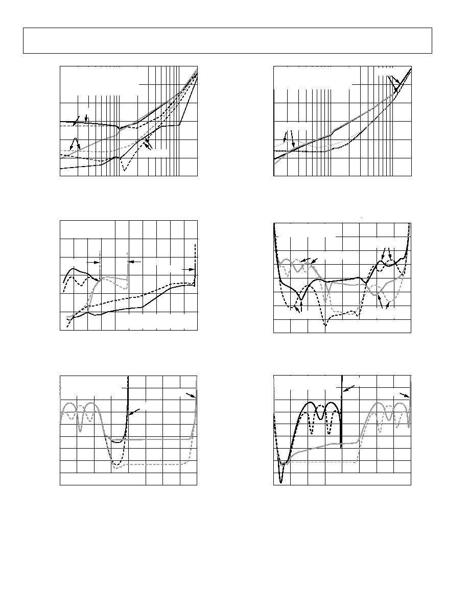
FREQUENCY (MHz)
0.1
1
20
10
DISTORTION (
d
B)
≠140
≠120
≠100
≠80
≠60
≠40
≠20
G = +1
V
OUT
= 2V p-p
R
L
= 1k
SECOND HARMONIC: SOLID LINE
THIRD HARMONIC: DASHED LINE
V
S
= +3V
V
S
= +5V
V
S
=
Ī5V
03327-A-020
Figure 21. Harmonic Distortion vs. Frequency and Supply Voltage
OUTPUT VOLTAGE (V p-p)
0
1
2
3
4
5
6
7
8
9
10
≠140
≠120
≠100
≠80
≠60
≠40
≠20
DISTORTION (
d
B)
G = +1 (R
F
= 24.9
)
FREQUENCY = 100kHz
R
L
= 1k
V
S
=
Ī5V
V
S
= +3V
V
S
= +5V
SECOND HARMONIC: SOLID LINE
THIRD HARMONIC: DASHED LINE
03327-A-021
Figure 22. Harmonic Distortion vs. Output Amplitude
INPUT COMMON-MODE VOLTAGE (V)
0.5
1.0
1.5
2.0
2.5
3.0
3.5
4.0
4.5
DISTORTION (
d
B)
≠140
≠130
≠120
≠110
≠100
≠90
≠80
≠70
≠60
≠50
G = +1 (R
F
= 24.9
)
V
OUT
= 1.0V p-p @ 100kHz
R
L
= 1k
SECOND HARMONIC: SOLID LINE
THIRD HARMONIC: DASHED LINE
V
S
= +3V
V
S
= +5V
03327-A-022
Figure 23. Harmonic Distortion vs. Input Common-Mode Voltage,
SELECT = High
FREQUENCY (MHz)
0.1
1
10
20
DISTORTION (
d
B)
≠140
≠120
≠100
≠80
≠60
≠40
≠20
G = +1 (R
F
= 24.9
)
V
OUT
= 2.0V p-p
SECOND HARMONIC: SOLID LINE
THIRD HARMONIC: DASHED LINE
R
L
= 150
R
L
= 1k
03327-A-023
Figure 24. Harmonic Distortion vs. Frequency and Load
INPUT COMMON-MODE VOLTAGE (V)
0.5
1.0
1.5
2.0
2.5
3.0
3.5
4.0
4.5
DISTORTION (
d
B)
≠125
≠115
≠105
≠95
≠85
≠75
≠65
≠55
≠45
G = +1 (R
F
= 24.9
)
V
OUT
= 1.0V p-p @ 2MHz
SELECT = HIGH
SELECT = TRI
SELECT = TRI
SELECT = HIGH
SECOND HARMONIC: SOLID LINE
THIRD HARMONIC: DASHED LINE
03327-A-024
Figure 25. Harmonic Distortion vs. Input Common-Mode Voltage, V
S
= +5 V
INPUT COMMON-MODE VOLTAGE (V)
0.5
1.0
1.5
2.0
2.5
3.0
3.5
4.0
4.5
DISTORTION (
d
B)
≠140
≠130
≠120
≠110
≠100
≠90
≠80
≠70
≠60
≠50
G = +1 (R
F
= 24.9
)
V
OUT
= 1.0V p-p @ 100kHz
SECOND HARMONIC: SOLID LINE
THIRD HARMONIC: DASHED LINE
V
S
= +3V
V
S
= +5V
03327-A-025
Figure 26. Harmonic Distortion vs. Input Common-Mode Voltage,
SELECT =
Tri
-State or Open
AD8027/AD8028
Rev. B | Page 11 of 24
FREQUENCY (MHz)
0.1
1
10
20
DISTORTION (
d
B)
≠140
≠120
≠100
≠80
≠60
≠40
≠20
V
S
= +5
V
OUT
= 2.0V p-p
SECOND HARMONIC: SOLID LINE
THIRD HARMONIC: DASHED LINE
G = +2
G = +1
G = +10
03327-A-026
Figure 27. Harmonic Distortion vs. Frequency and Gain
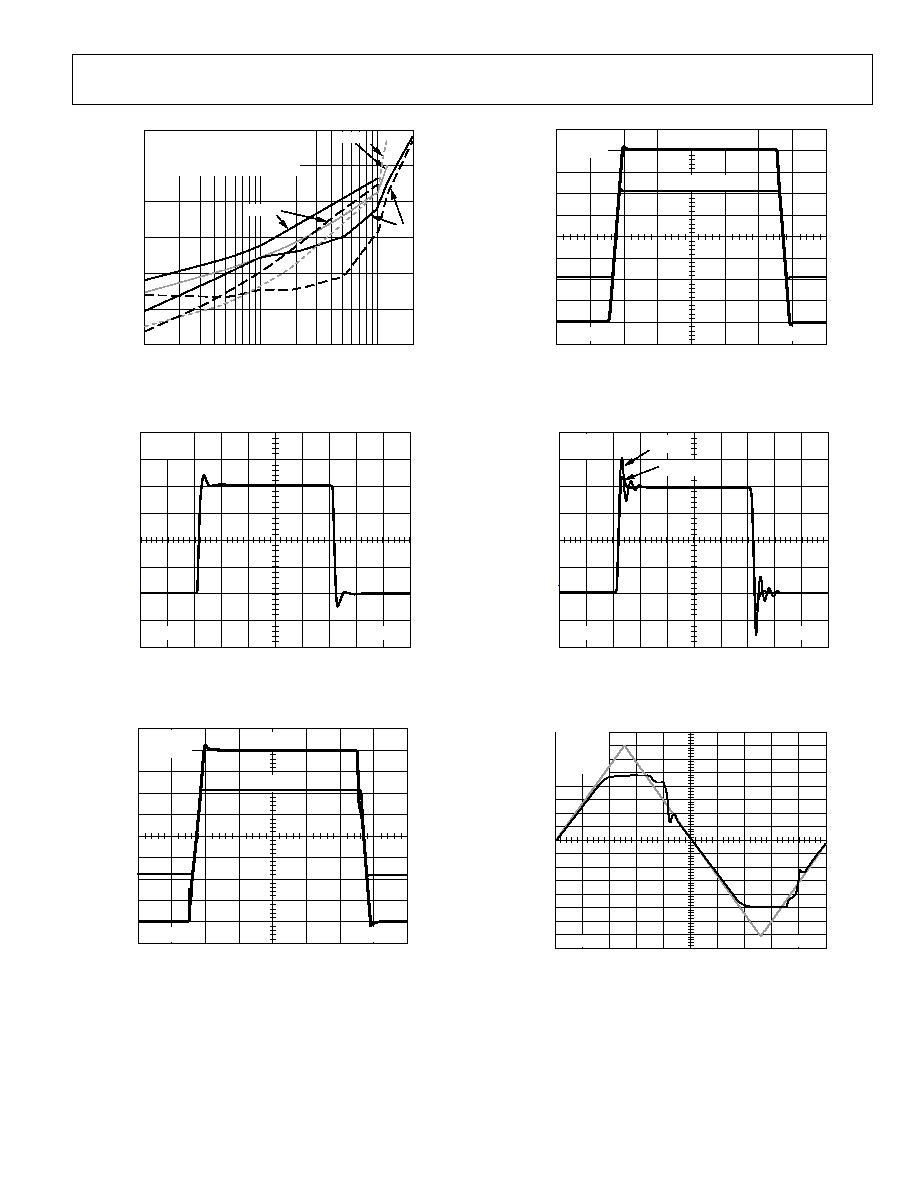
≠0.20
≠0.15
≠0.10
≠0.05
0.05
0
0.10
0.15
0.20
G = +1
V
S
= Ī 2.5V
20ns/DIV
50mV/DIV
03327-A-027
Figure 28. Small Signal Transient Response
≠2.0
≠1.0
0
1.0
2.0
100ns/DIV
500mV/DIV
G = +1
V
S
= Ī2.5V
V
OUT
= 4V p-p
V
OUT
= 2V p-p
03327-A-028
Figure 29. Large Signal Transient Response, G = +1
≠2.5
≠2.0
≠1.5
≠1.0
≠0.5
0
0.5
1.0
1.5
2.0
2.5
G = +2
V
S
= Ī2.5V
V
OUT
= 4V p-p
V
OUT
= 2V p-p
20ns/DIV
50mV/DIV
03327-A-029
Figure 30. Large Signal Transient Response, G = +2
≠0.20
≠0.15
≠0.10
≠0.05
0.05
0
0.10
0.15
0.20
G = +1
V
S
= Ī2.5V
C
L
= 20pF
C
L
= 5pF
20ns/DIV
50mV/DIV
03327-A-030
Figure 31. Small Signal Transient Response with Capacitive Load
≠4.0
≠3.0
≠2.0
≠1.0
0
1.0
2.0
3.0
4.0
≠3.5
≠2.5
≠1.5
≠0.5
0.5
1.5
2.5
3.5
50ns/DIV
500mV/DIV
G = ≠1
R
L
= 1k
V
S
=
Ī2.5V
03327-A-031
Figure 32. Output Overdrive Recovery
AD8027/AD8028
Rev. B | Page 12 of 24
≠4.0
≠3.0
≠2.0
≠1.0
0
1.0
2.0
3.0
4.0
≠3.5
≠2.5
≠1.5
≠0.5
0.5
1.5
2.5
3.5
50ns/DIV
500mV/DIV
G = +1
R
L
= 1k
V
S
=
Ī2.5V
03327-A-032
Figure 33. Input Overdrive Recovery
≠0.1%
+0.1%
5
Ķs/DIV
V
IN
(200mV/DIV)
V
OUT
≠ 2V
IN
(2mV/DIV)
G = +2
03327-A-033
Figure 34. Long-Term Settling Time
≠0.1%
+0.1%
20ns/DIV
V
IN
(200mV/DIV)
V
OUT
(400mV/DIV)
V
OUT
≠ 2V
IN
(0.1%/DIV)
03327-A-034
Figure 35. 0.1% Short-Term Settling Time
TEMPERATURE (įC)
INP
U
T BIAS
CURRE
NT (S
E
L
E
C
T = HIGH) (
Ķ
A)
≠40 ≠25 ≠10
5
20
35
50
65
80
110
95
125
2.5
3.0
3.5
4.0
4.5
INP
U
T BIAS
CURRE
NT (S
E
L
E
C
T = TRI) (
Ķ
A)
≠6.5
≠7.0
≠7.5
≠8.0
≠8.5
V
S
= +3V
V
S
= +5V
V
S
=
Ī5V
SELECT = TRI
SELECT = HIGH
03327-A-035
Figure 36. Input Bias Current vs. Temperature
INPUT COMMON-MODE VOLTAGE (V)
INP
U
T BIAS
CURRE
NT (
Ķ
A)
0
1
2
3
4
5
6
7
8
9
10
10
8
6
4
2
0
≠2
≠4
≠6
≠8
≠10
V
S
=
Ī5V
SELECT = TRI
V
S
= +3V
V
S
= +5V
SELECT = HIGH
03327-A-036
Figure 37. Input Bias Current vs. Input Common-Mode Voltage
≠800
≠600
≠400
≠200
0
200
400
600
800
INPUT OFFSET VOLTAGE (
ĶV)
0
50
100
150
200
250
FREQUENCY
SELECT = TRI
SELECT = HIGH
COUNT = 1780
SELECT
MEAN
STD. DEV
HIGH
49
ĶV
193
ĶV
TRI
55
ĶV
150
ĶV
03327-A-037
Figure 38. Input Offset Voltage Distribution

AD8027/AD8028
Rev. B | Page 13 of 24
TEMPERATURE (įC)
IN
PU
T OFFSET VOLTA
GE (
Ķ
V)
≠40 ≠25 ≠10
5
20
35
50
65
80
110
95
125
60
80
100
120
140
160
180
200
220
240
260
280
300
320
340
360
SELECT = TRI
V
S
=
Ī5V
V
S
= +5V
SELECT = HIGH
V
S
= +3V
03327-A-038
Figure 39. Input Offset Voltage vs. Temperature
INPUT COMMON-MODE VOLTAGE (V)
IN
PU
T OFFSET VOLTA
GE (
Ķ
V)
≠5
≠4
≠3
≠2
≠1
0
1
2
3
4
5
150
290
170
190
210
230
250
270
SELECT = HIGH
SELECT = TRI
V
S
=
Ī5V
03327-A-039
Figure 40. Input Offset Voltage vs. Input Common-Mode Voltage, V
S
= Ī5
INPUT COMMON-MODE VOLTAGE (V)
IN
PU
T OFFSET VOLTA
GE (
Ķ
V)
0
0.5
1.0
1.5
2.0
2.5
3.0
3.5
4.0
4.5
5.0
150
290
170
190
210
230
250
270
SELECT = HIGH
SELECT = TRI
V
S
= +5V
03327-A-040
Figure 41. Input Offset Voltage vs. Input Common-Mode Voltage, V
S
= +5
INPUT COMMON-MODE VOLTAGE (V)
INPUT OFFSET VOLTAGE (
Ķ
V)
0
0.50
1.00
1.50
2.00
2.50
3.00
150
270
170
190
210
230
250
SELECT = HIGH
SELECT = TRI
V
S
= +3V
03327-A-041
Figure 42. Input Offset Voltage vs. Input Common-Mode Voltage, V
S
= +3
FREQUENCY (Hz)
CMRR (dB)
1k
10k
100k
1M
10M
100M
0
20
40
60
80
100
120
03327-A-042
Figure 43. CMRR vs. Frequency
FREQUENCY (Hz)
PSSR
(
d
B
)
100
1k
10k
100k
1M
10M
100M
1G
≠110
≠100
≠90
≠80
≠70
≠60
≠50
≠40
≠30
≠20
≠10
0
≠PSRR
+PSRR
03327-A-043
Figure 44. PSRR vs. Frequency

AD8027/AD8028
Rev. B | Page 14 of 24
FREQUENCY (Hz)
OFF IS
OLATION (dB)
10k
100k
1M
10M
100M
1G
≠100
≠90
≠80
≠70
≠60
≠50
≠40
≠30
≠20
V
IN
= 0.2V p-p
G = +1
SELECT = LOW
03327-A-044
Figure 45. Off Isolation vs. Frequency
LOAD RESISTANCE (
)
OUTP
UT S
A
TURATION V
O
LTAGE
(mV
)
100
1000
10000
≠200
200
150
100
50
0
≠50
≠100
≠150
V
S
= +3V
V
S
= +5V V
S
=
Ī5V
V
OH
≠ V
S+
V
OL
≠ V
S≠
LOAD RESISTANCE TIED
TO MIDSUPPLY
03327-A-045
Figure 46. Output Saturation Voltage vs. Output Load
FREQUENCY (Hz)
1k
10k
100k
1M
10M
100M
1G
0.001
0.01
0.1
1
10
100
OUTP
UT IMP
E
DANCE
(
)
G = +2
G = +1
G = +5
03327-A-046
Figure 47. Output Enabled-- Impedance vs. Frequency
TEMPERATURE (įC)
OUTP
UT S
A
TURATION V
O
LTAGE
(mV
)
≠40 ≠25 ≠10
5
20
35
50
65
80
110
95
125
25
30
35
40
45
V
OL
≠ V
S≠
V
S
= +5V
R
L
= 1k
TIED TO MIDSUPPLY
V
S+
≠ V
OH
03327-A-047
Figure 48. Output Saturation Voltage vs. Temperature
I
LOAD
(mA)
OPEN-
L
OOP GAIN (
d
B)
0
10
20
30
40
50
60
60
130
70
80
90
100
110
120
Ī5V
+5V
+3V
03327-A-048
Figure 49. Open-Loop Gain vs. Load Current
FREQUENCY (Hz)
OUTP
UT IMP
E
DANCE
(
)
100k
1M
10M
100M
1G
10
100
1k
10k
100k
1M
SELECT = LOW
03327-A-049
Figure 50. Output Disabled--Impedance vs. Frequency

AD8027/AD8028
Rev. B | Page 15 of 24
SELECT VOLTAGE (V)
S
E
L
E
C
T CURRE
NT (
Ķ
A)
0
0.5
1.0
1.5
2.0
2.5
3.0
≠80
≠60
≠40
≠20
0
20
40
60
80
V
S
= +5V
V
S
= +10V
@ +25įC
+125įC
+25įC
≠40įC
03327-A-050
Figure 51. SELECT Pin Current vs.
SELECT Pin Voltage and Temperature
TIME (ns)
OUTPUT VOLTAGE (V)
0
50
100
150
200
250
≠1.5
≠1.0
≠0.5
0
0.5
1.0
1.5
SELECT PIN (≠2.0V TO ≠0.5V)
OUTPUT
R
L
= 1k
R
L
= 100
R
L
= 10k
G = ≠1
V
S
=
Ī2.5V
V
IN
= ≠1.0V
03327-A-051
Figure 52. Enable Turn-On Timing
TIME (
Ķs)
OUTPUT VOLTAGE (V)
0.5 1
2
3
4
5
6
7
8
9
10
≠1.5
≠1.0
≠0.5
0
0.5
1.0
1.5
G = ≠1
V
S
=
Ī2.5V
V
IN
= ≠1.0V
SELECT PIN (≠2.0V TO ≠0.5V)
R
L
= 1k
R
L
= 100
OUTPUT
R
L
= 10k
03327-A-052
Figure 53. Disable Turn-Off Timing
TEMPERATURE (įC)
S
U
P
P
L
Y
CURRE
NT (mA)
≠40 ≠25 ≠10
5
20
35
50
65
80
110
95
125
4.0
4.5
5.0
5.5
6.0
6.5
7.0
7.5
8.0
8.5
9.0
V
S
= +3V
V
S
= +5V
V
S
=
Ī5V
03327-A-053
Figure 54. Quiescent Supply Current vs. Supply Voltage and Temperature

AD8027/AD8028
Rev. B | Page 16 of 24
THEORY OF OPERATION
The AD8027/AD8028 is a rail-to-rail input and output amplifier
designed in Analog Devices XFCB process. The XFCB process
enables the AD8027/AD8028 to run on 2.7 V to 12 V supplies
with 190 MHz of bandwidth and over 100 V/Ķs of slew rate. The
AD8027/AD8028 has 4.3 nV/Hz of wideband noise with
17 nV/Hz noise at 10 Hz. This noise performance, with an
offset and drift performance of less than 900 ĶV maximum and
1.5 ĶV/įC typical, respectively, makes the AD8027/AD8028
ideal for high speed precision applications. Additionally, the
input stage operates 200 mV beyond the supply rails and shows
no phase reversal. The amplifier features overvoltage protection
on the input stage. Once the inputs exceed the supply rails by
0.7 V, ESD protection diodes will turn on, drawing excessive
current through the differential input pins. A series input resis-
tor should be included to limit the input current to less than
10 mA.
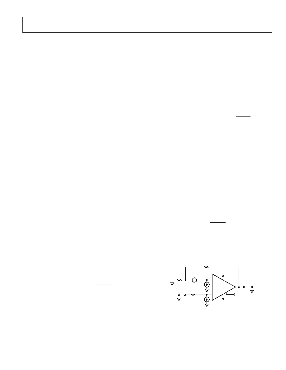
Input Stage
The rail-to-rail input performance is achieved by operating
complementary input pairs. Which pair is on is determined by
the common-mode level of the differential input signal. Look-
ing at the schematic in Figure 55, a tail current (I
TAIL
) is gener-
ated that sources the PNP differential input structure consisting
of Q1 and Q2. A reference voltage is generated internally that is
connected to the base of Q5. This voltage is continually com-
pared against the common-mode input voltage. When the
common-mode level exceeds the internal reference voltage, Q5
diverts the tail current (I
TAIL
) from the PNP input pair to a cur-
rent mirror that sources the NPN input pair consisting of Q3
and Q4. The NPN input pair can now operate 200 mV above
the positive rail. Both input pairs are protected from differential
input signals above 1.4 V by four diodes across the input (see
Figure 55). In the event of differential input signals that exceed
1.4 V, the diodes will conduct and excessive current will flow
through them. A series input resistor should be included to limit
the input current to 10 mA.
Crossover Selection
A new feature available on the AD8027/AD8028, which is called
Crossover Selection, allows the user to choose the crossover
point between the PNP/NPN differential pairs. Although the
crossover region is small, operating in this region should be
avoided since it can introduce offset and distortion to the out-
put signal. To help avoid operating in the crossover region, the
AD8027/AD8028 allows the user to select from two preset
crossover locations (i.e., voltage levels) using the SELECT pin.
Looking at the schematic in Figure 55, the crossover region is
about 200 mV and is defined by the voltage level at the base of
Q5. Internally, two separate voltage sources are created approxi-
mately 1.2 V from either rail. One or the other is connected to
Q5 based on the voltage applied to the SELECT pin. This allows
for either dominant PNP pair operation, when the SELECT pin
is left open, or dominant NPN pair operation, when the
SELECT pin is pulled high. This pin also provides the tradi-
tional power-down function when it is pulled low. This allows
the designer to achieve the best precision and ac performance
for high-side and low-side signal applications. See Figure 50
through Figure 53 for SELECT pin characteristics.
VCC
1.2V
+
≠
VEE
I
TAIL
1.2V
+
≠
LOGIC
VSEL
VP
Q5
Q3
Q1
Q2
Q4
VN
VOUTP
VOUTN
I
CMFB
VCC
VEE
I
CMFB
03327-A-054
Figure 55. Simplified Input Stage
AD8027/AD8028
Rev. B | Page 17 of 24
In the event that the crossover region cannot be avoided, spe-
cific attention has been given to the input stage to ensure con-
stant transconductance and minimal offset in all regions of
operation. The regions are: PNP input pair running, NPN input
pair running, and both running at the same time (in the
200 mV crossover region). Maintaining constant transconduc-
tance in all regions ensures the best wideband distortion per-
formance when going between these regions. With this tech-
nique, the AD8027/AD8028 can achieve greater than 80 dB
SFDR for a 2 V p-p, 1 MHz, G = +1 signal on Ī1.5 V supplies.
Another requirement in achieving this level of distortion is the
offset of each pair must be laser trimmed to achieve greater
than 80 dB SFDR, even for low frequency signals.
Output Stage
The AD8027/AD8028 uses a common-emitter output structure
to achieve rail-to-rail output capability. The output stage is
designed to drive 50 mA of linear output current, 40 mA within
200 mV of the rail, and 2.5 mA within 35 mV of the rail.
Loading of the output stage, including any possible feedback
network, will lower the open-loop gain of the amplifier. Refer to
Figure 49 for the loading behavior. Capacitive load can degrade
the phase margin of the amplifier. The AD8027/AD8028 can
drive up to 20 pF, G = +1 as seen in Figure 10. A small (25 to
50 ) series resistor (R
SNUB
) should be included if the capacitive
load is to exceed 20 pF for a gain of 1. Increasing the closed-
loop gain will increase the amount of capacitive load that can be
driven before a series resistor will need to be included.
DC Errors
The AD8027/AD8028 uses two complementary input stages to
achieve rail-to-rail input performance, as mentioned in the
Input Stage section. To use the dc performance over the entire
common-mode range, the input bias current and input offset
voltage of each pair must be considered.
Referring to Figure 56, the output offset voltage of each pair is
calculated by
+
=
G
F
G
PNP
OS
OUT
PNP
OS
R
R
R
V
V
,
,
,
,
+
=
G
F
G
NPN
OS
OUT
NPN
OS
R
R
R
V
V
,
,
,
where the difference of the two will be the discontinuity experi-
enced when going through the crossover region. The size of the
discontinuity is defined as
(
)
+
◊
-
=
G
F
G
NPN
OS,
PNP
OS,
DIS
R
R
R
V
V
V
Using the crossover select feature of the AD8027/AD8028 helps
to avoid this region. In the event that the region cannot be
avoided, the quantity (V
OS, PNP
≠ V
OS, NPN
) is trimmed to minimize
this effect.
Because the input pairs are complementary, the input bias
current will reverse polarity when going through the cross
over region shown in Figure 37. The offset between pairs is
described by
(
)
-
+
◊
-
=
-
F
G
F
G
S
NPN
B,
PNP
B,
NPN
OS,
PNP
OS,
R
R
R
R
R
I
I
V
V
I
B, PNP
is the input bias current of either input when the PNP
input pair is active, and I
B, NPN
is the input bias current or either
input pair when the NPN pair is active. If R
S
is sized so that
when multiplied by the gain factor it equals R
F
, this effect will be
eliminated. It is strongly recommended to balance the imped-
ances in this manner when traveling through the crossover
region to minimize the dc error and distortion. As an example,
assuming the PNP input pair has an input bias current of 6 ĶA
and the NPN input pair has an input bias current of ≠2 ĶA, a
200 ĶV shift in offset will occur when traveling through the
crossover region with R
F
equal to 0 and R
S
equal to 25 .
In addition to the input bias current shift between pairs, each
input pair has an input bias current offset that will contribute to
the total offset in the following manner
F
B
G
F
G
S
B
OS
R
I
R
R
R
R
I
V
-
+
-
+
=
V
OUT
I
B
+
R
F
R
G
I
B
≠
V
OS
R
S
+
≠
+
≠
V
I
+
≠
SELECT
≠V
+V
≠
+
AD8027/
AD8028
03327-A-055
Figure 56. Op Amp DC Error Sources

AD8027/AD8028
Rev. B | Page 18 of 24
WIDEBAND OPERATION
Voltage feedback amplifiers can use a wide range of resistor
values to set their gain. Proper design of the application's feed-
back network requires consideration of the following issues:
∑ Poles formed by the amplifier's input capacitances
with the resistances seen at the amplifier's input
terminals
∑ Effects of mismatched source impedances
∑ Resistor value impact on the application's voltage noise
∑ Amplifier loading effects
The AD8027/AD8028 has an input capacitance of 2 pF. This
input capacitance will form a pole with the amplifier's feedback
network, destabilizing the loop. For this reason, it is generally
desirable to keep the source resistances below 500 , unless
some capacitance is included in the feedback network. Likewise,
keeping the source resistances low will also take advantage of
the AD8027/AD8028's low input referred voltage noise of
4.3 nV/Hz.
With a wide bandwidth of over 190 MHz, the AD8027/AD8028
has numerous applications and configurations. The
AD8027/AD8028 shown in Figure 57 is configured as a nonin-
verting amplifier. The inverting configuration is shown in
Figure 58 and an easy selection table of gain, resistor values,
bandwidth, slew rate, and noise performance is presented in
Table 5.
+V
≠V
C2
10
ĶF
C1
0.1
ĶF
C4
0.1
ĶF
C3
10
ĶF
V
OUT
R
G
R1
R
F
SELECT
V
IN
R1 = R
F
||R
G
AD8027/
AD8028
+
≠
03327-A-056
Figure 57. Wideband Noninverting Gain Configuration
+V
≠V
C2
10
ĶF
C1
0.1
ĶF
C4
0.1
ĶF
C3
10
ĶF
R1
C5
V
OUT
R
G
R1 = R
F
||R
G
R
F
V
IN
SELECT
AD8027/
AD8028
+
≠
03327-A-057
C
F
Figure 58. Wideband Inverting Gain Configuration
Table 5. Component Values, Bandwidth, and Noise
Performance (V
S
=
Ī2.5 V)
Noise Gain
(Noninverting)
R
SOURCE
()
R
F
()
R
G
()
≠3 dB
SS BW
(MHz)
Output
Noise with
Resistors
(nV/Hz)
1 50
0
N/A
190
4.4
2 50
499
499
95
10
10 50
499
54.9
13
45

AD8027/AD8028
Rev. B | Page 19 of 24
Circuit Considerations
BALANCED INPUT IMPEDANCES
Balanced input impedances can help improve distortion per-
formance. When the amplifier transitions from PNP pair to
NPN pair operation, a change in both the magnitude and direc-
tion of the input bias current will occur. When multiplied times
imbalanced input impedances, a change in offset will result. The
key to minimizing this distortion is to keep the input imped-
ances balanced on both inputs. Figure 59 shows the effect of the
imbalance and degradation in distortion performance for a
50 source impedance, with and without a 50 balanced feed-
back path.
FREQUENCY (MHz)
0.1
1
10
20
DISTORTION (
d
B)
≠100
≠90
≠80
≠70
≠60
≠50
≠40
≠30
≠20
G = +1
V
OUT
= 2V p-p
R
L
= 1k
V
S
= +3V
R
F
= 24.9
R
F
= 49.9
R
F
= 0
03327-A-058
Figure 59. SFDR vs. Frequency and Various R
F
PCB LAYOUT
As with all high speed op amps, achieving optimum perform-
ance from the AD8027/AD8028 requires careful attention to
PCB layout. Particular care must be exercised to minimize lead
lengths of the bypass capacitors. Excess lead inductance can
influence the frequency response and even cause high fre-
quency oscillations. The use of a multilayer board, with an
internal ground plane, will reduce ground noise and enable a
tighter layout.
To achieve the shortest possible lead length at the inverting
input, the feedback resistor, R
F
,
should be located beneath the
board and span the distance from the output, Pin 6, to the input,
Pin 2. The return node of the resistor R
G
should be situated as
closely as possible to the return node of the negative supply
bypass capacitor connected to Pin 4.
On multilayer boards, all layers underneath the op amp should
be cleared of metal to avoid creating parasitic capacitive
elements. This is especially true at the summing junction (i.e.,
the ≠input). Extra capacitance at the summing junction can
cause increased peaking in the frequency response and lower
phase margin.
GROUNDING
To minimize parasitic inductances and ground loops in high
speed, densely populated boards, a ground plane layer is critical.
Understanding where the current flows in a circuit is critical in
the implementation of high speed circuit design. The length of
the current path is directly proportional to the magnitude of the
parasitic inductances and thus the high frequency impedance of
the path. Fast current changes in an inductive ground return
will create unwanted noise and ringing.
The length of the high frequency bypass capacitor pads and
traces is critical. A parasitic inductance in the bypass grounding
will work against the low impedance created by the bypass
capacitor. Because load currents flow from supplies as well as
ground, the load should be placed at the same physical location
as the bypass capacitor ground. For large values of capacitors,
which are intended to be effective at lower frequencies, the cur-
rent return path length is less critical.
POWER SUPPLY BYPASSING
Power supply pins are actually inputs and care must be taken to
provide a clean, low noise dc voltage source to these inputs. The
bypass capacitors have two functions:
1. Provide a low impedance path for unwanted frequencies
from the supply inputs to ground, thereby reducing the
effect of noise on the supply lines.
2. Provide sufficient localized charge storage, for fast
switching conditions and minimizing the voltage drop at
the supply pins and the output of the amplifier. This is
usually accomplished with larger electrolytic capacitors.
Decoupling methods are designed to minimize the bypassing
impedance at all frequencies. This can be accomplished with a
combination of capacitors in parallel to ground.
Good quality ceramic chip capacitors should be used and
always kept as close to the amplifier package as possible. A par-
allel combination of a 0.01 ĶF ceramic and a 10 ĶF electrolytic
covers a wide range of rejection for unwanted noise. The 10 ĶF
capacitor is less critical for high frequency bypassing, and in
most cases, one per supply line is sufficient.

AD8027/AD8028
Rev. B | Page 20 of 24
APPLICATIONS
Using the AD8027/AD8028 SELECT Pin
The AD8027/AD8028 features a unique SELECT pin with two
functions. The first is a power-down function that places the
AD8027/AD8028 into low power consumption mode. In the
power-down mode, the amplifier draws 450 ĶA (typ) of supply
current.
The second function, as mentioned in the Theory of Operation
section, shifts the crossover point (where the NPN/PNP input
differential pairs transition from one to the other) closer to
either the positive supply rail or the negative supply rail. This
selectable crossover point allows the user to minimize
distortion based on the input signal and environment. The
default state is 1.2 V from the positive power supply, with the
SELECT pin left floating or in tri-state.
Table 6 shows the required voltages and modes of the
SELECT pin.
Table 6. SELECT Pin Mode Control
SELECT Pin Voltage (V)
Mode
V
S
= Ī5 V
V
S
= +5 V
V
S
= +3 V
Disable
≠5 to ≠4.2
0 to 0.8
0 to 0.8
Crossover Referenced
≠1.2 V to Positive Supply
≠4.2 to ≠3.3
0.8 to 1.7
0.8 to 1.7
Crossover Referenced
+1.2 V to Negative Supply
≠3.3 to +5
1.7 to 5.0
1.7 to 3.0
When the input stage transitions from one input differential
pair to the other, there is virtually no noticeable change in the
output waveform.
The disable time of the AD8027/AD8028 amplifier is load
dependent. Typical data is presented in Table 7. See Figure 52
and Figure 53 for the actual switching measurements.
Table 7. DISABLE Switching Speeds
Supply Voltages
(R
L
= 1 k)
Ī5 V
+5 V
+3 V
t
ON
45 ns
50 ns
50 ns
t
OFF
980 ns
1100 ns
1150 ns
Driving a 16-Bit ADC
With the adjustable crossover distortion selection point and low
noise, the AD8028 is an ideal amplifier for driving or buffering
input signals into high resolution ADCs, such as the
AD7677,
a
16-Bit, 1 LSB INL, 1 MSPS differential ADC. Figure 60 shows
the typical schematic for driving the ADC.
The AD8028
driving the AD7677 offers performance close to non-rail-to-
rail amplifiers and avoids the need for an additional supply,
other than the single 5 V supply already used by the ADC.
In this application, the
SELECT
pins are biased to avoid the
crossover region of the AD8028 for low distortion
operation.
+5V
+5V
+
≠
AD8028
ANALOG INPUT +
INPUT RANGE
(0.15V TO 2.65V)
SELECT
(OPEN)
SELECT
(OPEN)
+
≠
ANALOG INPUT ≠
AD7677
+5V
16 BITS
15
15
2.7nF
4MHz LPF
4MHz LPF
2.7nF
0.1
ĶF
0.1
ĶF
AD8028
03327-A-059
Figure 60. Unity Gain Differential Drive
As seen in Figure 61, the AD8028 and AD7677 combination
offers excellent integral nonlinearity (INL). Summary test data
for the schematic shown in Figure 60 is presented in Table 8.
Table 8. ADC Driver Performance,
f
C
= 100 kHz, V
OUT
= 4.7 V p-p
Parameter Measurement
Second Harmonic Distortion
≠105dB
Third Harmonic Distortion
≠102dB
THD ≠102
dB
SFDR 105
dBc
CODE
0
16384
32768
49152
65536
≠1.0
≠0.5
0
0.5
1.0
INL (
L
SB)
03327-A-060
Figure 61. Integral Nonlinearity

AD8027/AD8028
Rev. B | Page 21 of 24
Band-Pass Filter
In communication systems, active filters are used extensively in
signal processing. The AD8027/AD8028 is an excellent choice
for active filter applications. In realizing this filter, it is impor-
tant that the amplifier has a large signal bandwidth of at least
10◊ the center frequency, f
O
. Otherwise, a phase shift can occur
in the amplifier, causing instability and oscillations.
In the schematic shown in Figure 62, the AD8027/AD8028 is
configured as a 1 MHz band-pass filter. The target specifications
are f
O
= 1 MHz and a ≠3 dB pass band of 500 kHz. Start the
design by selecting the following: f
O
, Q, C1, and R4. Then using
the equations shown below, calculate the remaining variables.
The test data shown in Figure 63 indicates that this design
yielded a filter response with a center frequency f
O
= 1 MHz and
a bandwidth of 450 kHz.
(MHz)
(MHz)
Band
Pass
f
Q
O
=
k = 2f
O
C1
C2 = 0.5C1
R1 = 2/k, R2 = 2/(3k), R3 = 4/k
H = 1/3(6.5 ≠ 1/Q)
R5 = R4/(H ≠ 1)
+5
≠5
C3
0.1
ĶF
C4
0.1
ĶF
R4
523
R5
523
C2
500pF
C1
1000pF
R3
634
V
OUT
R1
316
R2
105
V
IN
SELECT
AD8027/
AD8028
+
≠
03327-A-061
Figure 62. Band-Pass Filter Schematic
0.1
CH1 S21 LOG
5dB/REF 6.342dB
1:6.3348dB 1.00 000MHz
1
FREQUENCY ≠ MHz
10
1
03327-A-062
Figure 63. Band-Pass Filter Response
Design Tools and Technical Support
Analog Devices is committed to simplifying the design process
by providing technical support and online design tools. We offer
technical support via free evaluation boards, sample ICs, inter-
active evaluation tools, data sheets, spice models, application
notes, phone and email support, all of which are available at
www. analog.com
.
AD8027/AD8028
Rev. B | Page 22 of 24
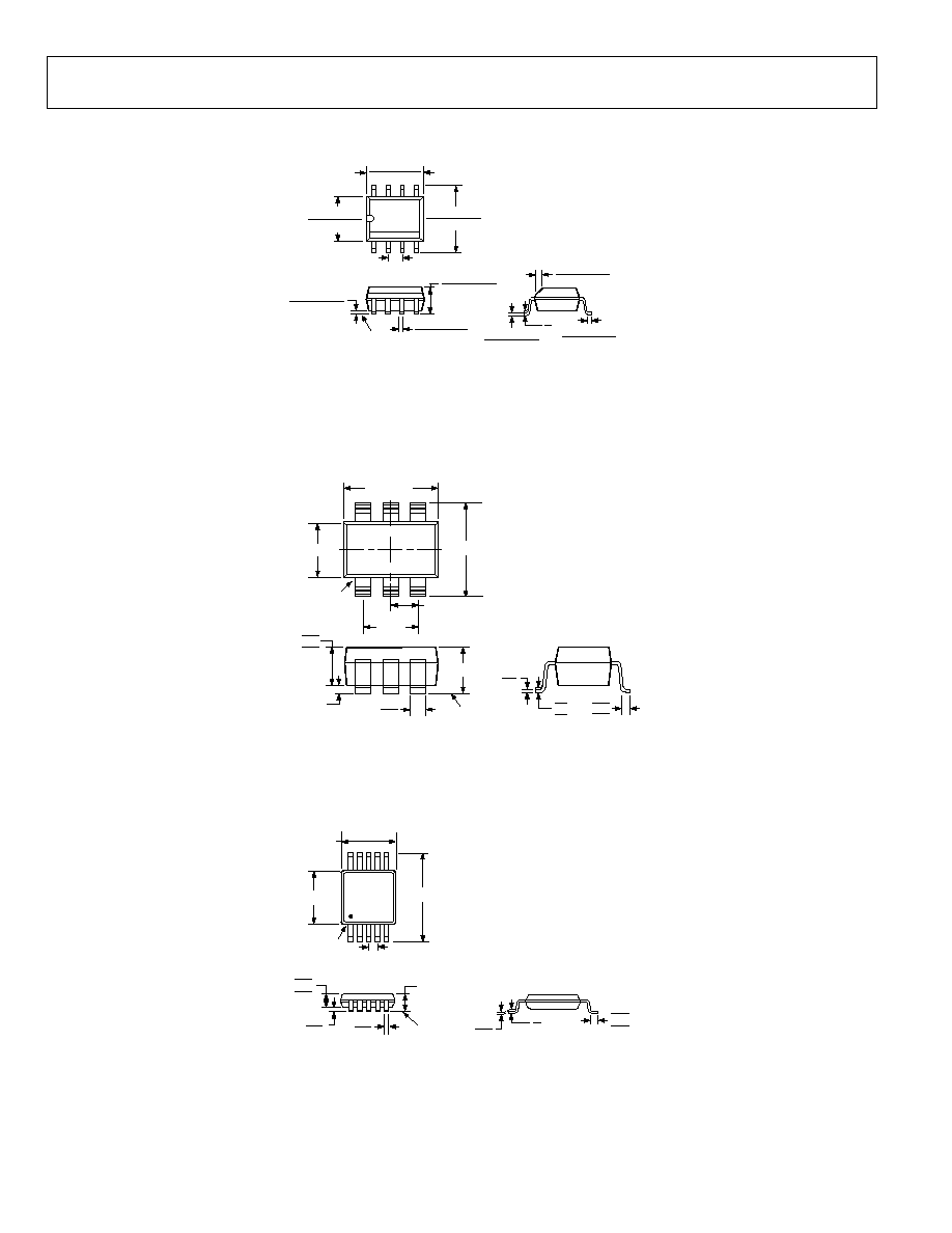
OUTLINE DIMENSIONS
0.25 (0.0098)
0.17 (0.0067)
1.27 (0.0500)
0.40 (0.0157)
0.50 (0.0196)
0.25 (0.0099)
◊ 45į
8į
0į
1.75 (0.0688)
1.35 (0.0532)
SEATING
PLANE
0.25 (0.0098)
0.10 (0.0040)
4
1
8
5
5.00 (0.1968)
4.80 (0.1890)
4.00 (0.1574)
3.80 (0.1497)
1.27 (0.0500)
BSC
6.20 (0.2440)
5.80 (0.2284)
0.51 (0.0201)
0.31 (0.0122)
COPLANARITY
0.10
CONTROLLING DIMENSIONS ARE IN MILLIMETERS; INCH DIMENSIONS
(IN PARENTHESES) ARE ROUNDED-OFF MILLIMETER EQUIVALENTS FOR
REFERENCE ONLY AND ARE NOT APPROPRIATE FOR USE IN DESIGN
COMPLIANT TO JEDEC STANDARDS MS-012AA
Figure 64. 8-Lead Standard Small Outline Package, Narrow Body [SOIC]
(R-8)
Dimensions shown in millimeters and (inches)
1
3
4
5
2
6
2.90 BSC
PIN 1
1.60 BSC
2.80 BSC
1.90
BSC
0.95 BSC
0.22
0.08
0.60
0.45
0.30
10į
4į
0į
0.50
0.30
0.15 MAX
1.30
1.15
0.90
SEATING
PLANE
1.45 MAX
COMPLIANT TO JEDEC STANDARDS MO-178AB
Figure 65. 6-Lead Plastic Surface-Mount Package [SOT-23]
(RT-6)
Dimensions shown in millimeters
0.23
0.08
0.80
0.60
0.40
8į
0į
0.15
0.00
0.27
0.17
0.95
0.85
0.75
SEATING
PLANE
1.10 MAX
10
6
5
1
0.50 BSC
3.00 BSC
3.00 BSC
4.90 BSC
PIN 1
COPLANARITY
0.10
COMPLIANT TO JEDEC STANDARDS MO-187BA
Figure 66. 10-Lead Mini Small Outline Package [MSOP]
(RM-10)
Dimensions shown in millimeters

AD8027/AD8028
Rev. B | Page 23 of 24
ESD CAUTION
ESD (electrostatic discharge) sensitive device. Electrostatic charges as high as 4000 V readily accumulate on
the human body and test equipment and can discharge without detection. Although this product features
proprietary ESD protection circuitry, permanent damage may occur on devices subjected to high energy
electrostatic discharges. Therefore, proper ESD precautions are recommended to avoid performance
degradation or loss of functionality.
Ordering Guide
Model
Minimum Ordering Quantity
Temperature Range Package
Description Package
Outline Branding
AD8027AR
1
≠40įC to +125įC
8-Lead SOIC
R-8
AD8027AR-REEL
2,500
≠40įC to +125įC
8-Lead SOIC
R-8
AD8027AR-REEL7
1,000
≠40įC to +125įC
8-Lead SOIC
R-8
AD8027ART-R2
250
≠40įC to +125įC
6-Lead SOT-23
RT-6
H4B
AD8027ART-REEL
10,000
≠40įC to +125įC
6-Lead SOT-23
RT-6
H4B
AD8027ART-REEL7
3,000
≠40įC to +125įC
6-Lead SOT-23
RT-6
H4B
AD8028AR
1
≠40įC to +125įC
8-Lead SOIC
R-8
AD8028AR-REEL
2,500
≠40įC to +125įC
8-Lead SOIC
R-8
AD8028AR-REEL7
1,000
≠40įC to +125įC
8-Lead SOIC
R-8
AD8028ARM
1
≠40įC to +125įC
10-Lead MSOP
RM-10
H5B
AD8028ARM-REEL
3,000
≠40įC to +125įC
10-Lead MSOP
RM-10
H5B
AD8028ARM-REEL7
1,000
≠40įC to +125įC
10-Lead MSOP
RM-10
H5B

AD8027/AD8028
Rev. B | Page 24 of 24
NOTES
© 2003 Analog Devices, Inc. All rights reserved. Trademarks and
regis-
tered trademarks are the property of their respective owners.
C03327≠0≠10/03(B)