 | ÐлекÑÑоннÑй компоненÑ: AD8042 | СкаÑаÑÑ:  PDF PDF  ZIP ZIP |
Äîêóìåíòàöèÿ è îïèñàíèÿ www.docs.chipfind.ru
CONNECTION DIAGRAM
8-Lead Plastic DIP and SOIC
OUT1
IN1
+IN1
V
S
OUT2
+V
S
IN2
+IN2
1
2
3
4
8
7
6
5
AD8042
REV. A
Information furnished by Analog Devices is believed to be accurate and
reliable. However, no responsibility is assumed by Analog Devices for its
use, nor for any infringements of patents or other rights of third parties
which may result from its use. No license is granted by implication or
otherwise under any patent or patent rights of Analog Devices.
a
Dual 160 MHz
Rail-to-Rail Amplifier
AD8042
FEATURES
Single AD8041 and Quad AD8044 also Available
Fully Specified at +3 V, +5 V, and 5 V Supplies
Output Swings to Within 30 mV of Either Rail
Input Voltage Range Extends 200 mV Below Ground
No Phase Reversal with Inputs 0.5 V Beyond Supplies
Low Power of 5.2 mA per Amplifier
High Speed and Fast Settling on +5 V:
160 MHz 3 dB Bandwidth (G = +1)
200 V/ s Slew Rate
39 ns Settling Time to 0.1%
Good Video Specifications (R
L
= 150 , G = +2)
Gain Flatness of 0.1 dB to 14 MHz
0.02% Differential Gain Error
0.04 Differential Phase Error
Low Distortion
64 dBc Worst Harmonic @ 10 MHz
Drives 50 mA 0.5 V from Supply Rails
APPLICATIONS
Video Switchers
Distribution Amplifiers
A/D Driver
Professional Cameras
CCD Imaging Systems
Ultrasound Equipment (Multichannel)
PRODUCT DESCRIPTION
The AD8042 is a low power voltage feedback, high speed am-
plifier designed to operate on +3 V, +5 V or
±
5 V supplies. It
has true single supply capability with an input voltage range
extending 200 mV below the negative rail and within 1 V of the
positive rail.
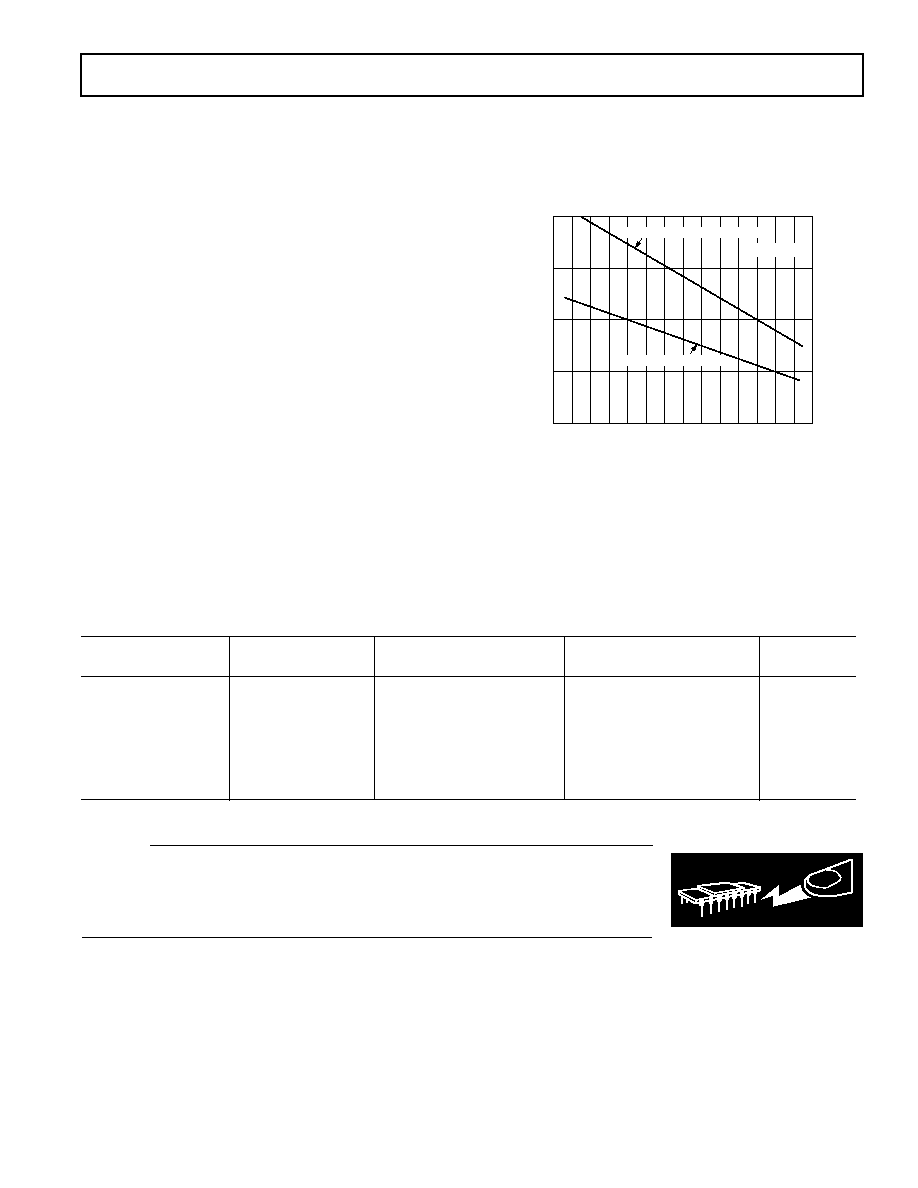
5V
2.5V
0V
1 s
1V
G = 1
R
L
= 2k TO +2.5V
Figure 1. Output Swing: Gain = 1, V
S
= +5 V
The output voltage swing extends to within 30 mV of each rail,
providing the maximum output dynamic range. Additionally, it
features gain flatness of 0.1 dB to 14 MHz while offering differ-
ential gain and phase error of 0.04% and 0.06
°
on a single +5 V
supply. This makes the AD8042 useful for professional video
electronics such as cameras, video switchers or any high speed
portable equipment. The AD8042's low distortion and fast
settling make it ideal for buffering single supply, high speed
A-to-D converters.
The AD8042 offers low power supply current of 12 mA max
and can run on a single +3.3 V power supply. These features are
ideally suited for portable and battery powered applications
where size and power are critical.
The wide bandwidth of 160 MHz along with 200 V/
µ
s of slew
rate on a single +5 V supply make the AD8042 useful in many
general purpose, high speed applications where single supplies
from +3.3 V to +12 V and dual power supplies of up to
±
6 V
are needed. The AD8042 is available in 8-lead plastic DIP and
SOIC.
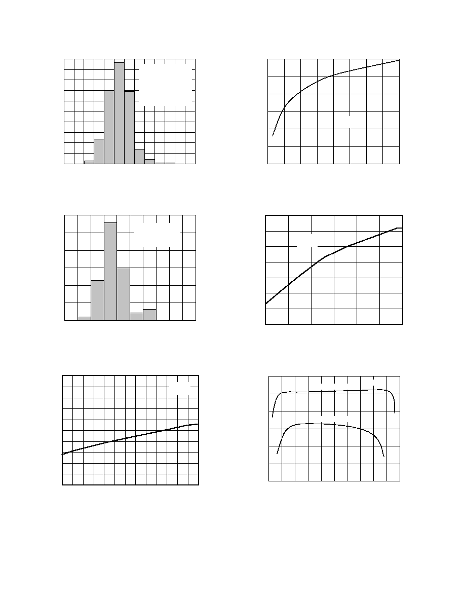
15
CLOSEDLOOP GAIN dB
12
9
6
3
0
3
6
9
12
15
1
10
100
500
FREQUENCY MHz
V
S
= +5V
G = +1
C
L
= 5pF
R
L
= 2k TO 2.5V
Figure 2. Frequency Response
One Technology Way, P.O. Box 9106, Norwood, MA 02062-9106, U.S.A.
Tel: 781/329-4700
World Wide Web Site: http://www.analog.com
Fax: 781/326-8703
© Analog Devices, Inc., 1999

AD8042SPECIFICATIONS
(@ T
A
= +25 C, V
S
= +5 V, R
L
= 2 k to 2.5 V, unless otherwise noted)
AD8042A
Parameter
Conditions
Min
Typ
Max
Units
DYNAMIC PERFORMANCE
3 dB Small Signal Bandwidth, V
O
< 0.5 V p-p
G = +1
125
160
MHz
Bandwidth for 0.1 dB Flatness
G = +2, R
L
= 150
. R
F
= 200
14
MHz
Slew Rate
G = 1, V
O
= 2 V Step
130
200
V/
µ
s
Full Power Response
V
O
= 2 V p-p
30
MHz
Settling Time to 1%
G = 1, V
O
= 2 V Step
26
ns
Settling Time to 0.1%
39
ns
NOISE/DISTORTION PERFORMANCE
Total Harmonic Distortion
f
C
= 5 MHz, V
O
= 2 V p-p, G = +2, R
L
= 1 k
73
dB
Input Voltage Noise
f = 10 kHz
15
nV/
Hz
Input Current Noise
f = 10 kHz
700
fA/
Hz
Differential Gain Error (NTSC, 100 IRE)
G = +2, R
L
= 150
to 2.5 V
0.04
0.06
%
G = +2, R
L
= 75
to 2.5 V
0.04
%
Differential Phase Error (NTSC, 100 IRE)
G = +2, R
L
= 150
to 2.5 V
0.06
0.12
Degrees
G = +2, R
L
= 75
to 2.5 V
0.24
Degrees
Worst Case Crosstalk
f = 5 MHz, R
L
= 150
to 2.5 V
63
dB
DC PERFORMANCE
Input Offset Voltage
3
9
mV
T
MIN
T
MAX
12
mV
Offset Drift
12
µ
V/
°
C
Input Bias Current
1.2
3.2
µ
A
T
MIN
T
MAX
4.8
µ
A
Input Offset Current
0.2
0.5
µ
A
Open-Loop Gain
R
L
= 1 k
90
100
dB
T
MIN
T
MAX
90
dB
INPUT CHARACTERISTICS
Input Resistance
300
k
Input Capacitance
1.5
pF
Input Common-Mode Voltage Range
0.2 to 4
V
Common-Mode Rejection Ratio
V
CM
= 0 V to 3.5 V
68
74
dB
OUTPUT CHARACTERISTICS
Output Voltage Swing
R
L
= 10 k
to 2.5 V
0.03 to 4.97
V
Output Voltage Swing:
R
L
= 1 k
to 2.5 V
0.10 to 4.9
0.05 to 4.95
V
Output Voltage Swing:
R
L
= 50
to 2.5 V
0.4 to 4.4
0.36 to 4.45
V
Output Current
T
MIN
to T
MAX,
V
OUT
= 0.5 V to 4.5 V
50
mA
Short Circuit Current
Sourcing
90
mA
Sinking
100
mA
Capacitive Load Drive
G = +1
20
pF
POWER SUPPLY
Operating Range
3
12
V
Quiescent Current (Per Amplifier)
5.2
6
mA
Power Supply Rejection Ratio
V
S
= 0 V to 1 V, or V
S+
= +5 V to +6 V
72
80
dB
OPERATING TEMPERATURE RANGE
40
+85
°
C
Specifications subject to change without notice.
REV. A
2

AD8042
SPECIFICATIONS
(@ T
A
= +25 C, V
S
= +3 V, R
L
= 2 k to 1.5 V, unless otherwise noted)
AD8042A
Parameter
Conditions
Min
Typ
Max
Units
DYNAMIC PERFORMANCE
3 dB Small Signal Bandwidth, V
O
< 0.5 V p-p
G = +1
120
140
MHz
Bandwidth for 0.1 dB Flatness
G = +2, R
L
= 150
, R
F
= 200
11
MHz
Slew Rate
G = 1, V
O
= 2 V Step
120
170
V/
µ
s
Full Power Response
V
O
= 2 V p-p
25
MHz
Settling Time to 1%
G = 1, V
O
= 1 V Step
30
ns
Settling Time to 0.1%
45
ns
NOISE/DISTORTION PERFORMANCE
Total Harmonic Distortion
f
C
= 5 MHz, V
O
= 2 V p-p, G = 1, R
L
= 100
56
dB
Input Voltage Noise
f = 10 kHz
16
nV/
Hz
Input Current Noise
f = 10 kHz
500
fA/
Hz
Differential Gain Error (NTSC, 100 IRE)
G = +2, R
L
= 150
to 1.5 V, Input V
CM
= 1 V
0.10
%
R
L
= 75
to 1.5 V, Input V
CM
= 1 V
0.10
%
Differential Phase Error (NTSC, 100 IRE)
G = +2, R
L
= 150
to 1.5 V, Input V
CM
= 1 V
0.12
Degrees
R
L
= 75
to 1.5 V, Input V
CM
= 1 V
0.27
Degrees
Worst Case Crosstalk
f = 5 MHz, R
L
= 1 k
to 1.5 V
68
dB
DC PERFORMANCE
Input Offset Voltage
3
9
mV
T
MIN
T
MAX
12
mV
Offset Drift
12
µ
V/
°
C
Input Bias Current
1.2
3.2
µ
A
T
MIN
T
MAX
4.8
µ
A
Input Offset Current
0.2
0.6
µ
A
Open-Loop Gain
R
L
= 1 k
90
100
dB
T
MIN
T
MAX
90
dB
INPUT CHARACTERISTICS
Input Resistance
300
k
Input Capacitance
1.5
pF
Input Common-Mode Voltage Range
0.2 to 2
V
Common-Mode Rejection Ratio
V
CM
= 0 V to 1.5 V
66
74
dB
OUTPUT CHARACTERISTICS
Output Voltage Swing
R
L
= 10 k
to 1.5 V
0.03 to 2.97
V
Output Voltage Swing:
R
L
= 1 k
to 1.5 V
0.1 to 2.9
0.05 to 2.95
V
Output Voltage Swing:
R
L
= 50
to 1.5 V
0.3 to 2.6
0.25 to 2.65
V
Output Current
T
MIN
to T
MAX,
V
OUT
= 0.5 V to 2.5 V
50
mA
Short Circuit Current
Sourcing
50
mA
Sinking
70
mA
Capacitive Load Drive
G = +1
17
pF
POWER SUPPLY
Operating Range
3
12
V
Quiescent Current (Per Amplifier)
5.0
6
mA
Power Supply Rejection Ratio
V
S
= 0 V to 1 V, or V
S+
= +3 V to +4 V
68
80
dB
OPERATING TEMPERATURE RANGE
0
+70
°
C
Specifications subject to change without notice.
REV. A
3

REV. A
4
AD8042A
Parameter
Conditions
Min
Typ
Max
Units
DYNAMIC PERFORMANCE
3 dB Small Signal Bandwidth, V
O
< 0.5 V p-p
G = +1
125
170
MHz
Bandwidth for 0.1 dB Flatness
G = +2, R
L
= 150
, R
F
= 200
18
MHz
Slew Rate
G = 1, V
O
= 2 V Step
145
225
V/
µ
s
Full Power Response
V
O
= 2 V p-p
35
MHz
Settling Time to 1%
G = 1, V
O
= 2 V Step
22
ns
Settling Time to 0.1%
32
ns
NOISE/DISTORTION PERFORMANCE
Total Harmonic Distortion
f
C
= 5 MHz, V
O
= 2 V p-p, G = +2, R
L
= 1 k
78
dB
Input Voltage Noise
f = 10 kHz
15
nV/
Hz
Input Current Noise
f = 10 kHz
700
fA/
Hz
Differential Gain Error (NTSC, 100 IRE)
G = +2, R
L
= 150
0.02
0.05
%
G = +2, R
L
= 75
0.02
%
Differential Phase Error (NTSC, 100 IRE)
G = +2, R
L
= 150
0.04
0.10
Degrees
G = +2, R
L
= 75
0.12
Degrees
Worst Case Crosstalk
f = 5 MHz, R
L
= 150
63
dB
DC PERFORMANCE
Input Offset Voltage
3
9.8
mV
T
MIN
T
MAX
14
mV
Offset Drift
12
µ
V/
°
C
Input Bias Current
1.2
3.2
µ
A
T
MIN
T
MAX
4.8
µ
A
Input Offset Current
0.2
0.6
µ
A
Open-Loop Gain
R
L
= 1 k
90
94
dB
T
MIN
T
MAX
86
dB
INPUT CHARACTERISTICS
Input Resistance
300
k
Input Capacitance
1.5
pF
Input Common-Mode Voltage Range
5.2 to 4
V
Common-Mode Rejection Ratio
V
CM
= 5 V to 3.5 V
66
74
dB
OUTPUT CHARACTERISTICS
Output Voltage Swing
R
L
= 10 k
4.97 to +4.97
V
Output Voltage Swing:
R
L
= 1 k
4.8 to +4.8
4.9 to +4.9
V
Output Voltage Swing:
R
L
= 50
4 to +3.2
4.2 to +3.5
V
Output Current
T
MIN
to T
MAX,
V
OUT
= 4.5 V to 4.5 V
50
mA
Short Circuit Current
Sourcing
100
mA
Sinking
100
mA
Capacitive Load Drive
G = +1
25
pF
POWER SUPPLY
Operating Range
3
12
V
Quiescent Current (Per Amplifier)
6
7
mA
Power Supply Rejection Ratio
V
S
= 5 V to 6 V, or V
S+
= +5 V to +6 V
68
80
dB
OPERATING TEMPERATURE RANGE
40
+85
°
C
Specifications subject to change without notice.
(@ T
A
= +25 C, V
S
= 5 V, R
L
= 2 k
to 0 V, unless otherwise noted)
AD8042SPECIFICATIONS
AD8042
REV. A
5
ABSOLUTE MAXIMUM RATINGS
1
Supply Voltage . . . . . . . . . . . . . . . . . . . . . . . . . . . . . . . +12.6 V
Internal Power Dissipation
2
Plastic DIP Package (N) . . . . . . . . . . . . . . . . . . . 1.3 Watts
Small Outline Package (R) . . . . . . . . . . . . . . . . . . 0.9 Watts
Input Voltage (Common Mode) . . . . . . . . . . . . . .
±
V
S
±
0.5 V
Differential Input Voltage . . . . . . . . . . . . . . . . . . . . . . .
±
3.4 V
Output Short Circuit Duration
. . . . . . . . . . . . . . . . . . . . . . Observe Power Derating Curves
Storage Temperature Range (N, R) . . . . . . . 65
°
C to +125
°
C
Lead Temperature Range (Soldering 10 sec) . . . . . . . . +300
°
C
NOTES
1
Stresses above those listed under Absolute Maximum Ratings may cause perma-
nent damage to the device. This is a stress rating only; functional operation of the
device at these or any other conditions above those indicated in the operational
section of this specification is not implied. Exposure to absolute maximum rating
conditions for extended periods may affect device reliability.
2
Specification is for the device in free air:
8-Lead Plastic DIP Package:
JA
= 90
°
C/W
8-Lead SOIC Package:
JA
= 155
°
C/W
MAXIMUM POWER DISSIPATION
The maximum power that can be safely dissipated by the
AD8042 is limited by the associated rise in junction tempera-
ture. The maximum safe junction temperature for plastic encap-
sulated devices is determined by the glass transition temperature
of the plastic, approximately +150
°
C. Exceeding this limit tem-
porarily may cause a shift in parametric performance due to a
change in the stresses exerted on the die by the package.
Exceeding a junction temperature of +175
°
C for an extended
period can result in device failure.
While the AD8042 is internally short circuit protected, this may
not be sufficient to guarantee that the maximum junction
temperature (+150
°
C) is not exceeded under all conditions.
To ensure proper operation, it is necessary to observe the
maximum power derating curves.
MAXIMUM POWER DISSIPATION Watts
AMBIENT TEMPERATURE C
2.0
1.5
0
50
90
40 30 20 10
0
10 20
30
50 60
70 80
40
1.0
0.5
8-LEAD PLASTIC-DIP PACKAGE
8-LEAD SOIC PACKAGE
T
J
= +150 C
Figure 3. Maximum Power Dissipation vs. Temperature
CAUTION
ESD (electrostatic discharge) sensitive device. Electrostatic charges as high as 4000 V readily
accumulate on the human body and test equipment and can discharge without detection.
Although the AD8042 features proprietary ESD protection circuitry, permanent damage may
occur on devices subjected to high energy electrostatic discharges. Therefore, proper ESD
precautions are recommended to avoid performance degradation or loss of functionality.
ORDERING GUIDE
Supply
Temperature
Package
Package
Model
Voltages
Range
Description
Option
AD8042AN
+5 V,
±
5 V
40
°
C to +85
°
C
8-Lead Plastic DIP
N-8
AD8042AN
+3 V
0
°
C to +70
°
C
8-Lead Plastic DIP
N-8
AD8042AR
+5 V,
±
5 V
40
°
C to +85
°
C
8-Lead Plastic SOIC
SO-8
AD8042AR
+3 V
0
°
C to +70
°
C
8-Lead Plastic SOIC
SO-8
AD8042AR-REEL
40
°
C to +85
°
C
13" Tape and REEL
SO-8
AD8042AR-REEL7
40
°
C to +85
°
C
7" Tape and REEL
SO-8
AD8042ACHIPS
40
°
C to +85
°
C
Die
WARNING!
ESD SENSITIVE DEVICE
V
S
= +5V
T = +25 C
140 PARTS, SIDE A & B
MEAN = 1.52mV
STD DEVIATION = 1.15
SAMPLE SIZE = 280
(140 AD8042S)
V
OS
mV
100
40
0
80
60
20
90
70
50
30
10
6
6
5
4
3
2
1
0
1
2
3
4
5
FREQUENCY
Figure 4. Typical Distribution of V
OS
V
OS
DRIFT V/ C
20
15
0
18
4
16
FREQUENCY
14
12
0
8
6
2
10
5
V
S
= +5V
MEAN = 12.6 V/ C
STD DEV = 2.02 V/ C
SAMPLE SIZE = 60
10
25
30
Figure 5. V
OS
Drift Over 40
°
C to +85
°
C
INPUT BIAS CURRENT
A
TEMPERATURE C
0
0.2
0.4
0.6
0.8
1
1.2
1.4
1.6
1.8
2
40 30 20 10
0
10
20
30
40
50
60
70
80
V
S
= +5V
V
CM
= 0V
90
Figure 6. I
B
vs. Temperature
AD8042Typical Performance Characteristics
6
REV. A
LOAD RESISTANCE
100
70
95
90
85
80
75
0
2000
250
500
750
1000
1250
1500
1750
V
S
= +5V
T = +25 C
OPEN-LOOP GAIN dB
Figure 7. Open-Loop Gain vs. R
L
to +2.5 V
100
98
96
94
92
90
88
86
40
20
0
20
40
60
80
TEMPERATURE C
OPEN-LOOP GAIN dB
V
S
= +5V
R
L
= 1k
Figure 8. Open-Loop Gain vs. Temperature
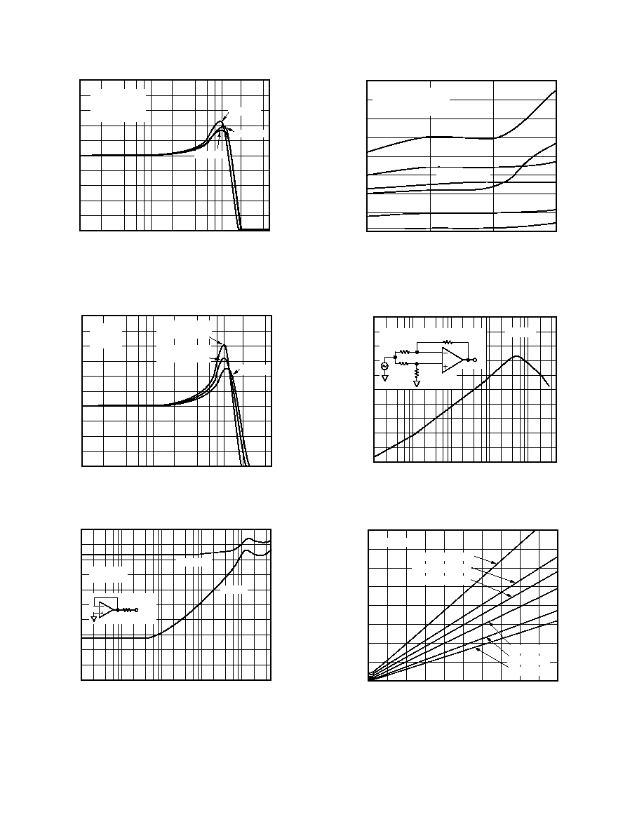
OUTPUT VOLTAGE Volts
100
70
40
90
80
60
50
0
5
0.5
1
1.5
2
2.5
3
3.5
4
4.5
R
L
= 500 TO 2.5V
V
S
= +5V
R
L
= 50 TO 2.5V
OPEN-LOOP GAIN dB
Figure 9. Open-Loop Gain vs. Output Voltage
AD8042
REV. A
7
10
100
1k
10k
100k
1M
10M
100M
1G
300
100
30
10
3
1
FREQUENCY Hz
INPUT VOLTAGE NOISE nV/ Hz
Figure 10. Input Voltage Noise vs. Frequency
FUNDAMENTAL FREQUENCY MHz
30
40
100
1
10
3
TOTAL HARMONIC DISTORTION dBc
50
70
80
60
2
4
5
6
7 8 9
90
V
S
= +5V, A
V
= +1,
R
L
= 1k TO 2.5V
V
S
= +5V, A
V
= +2,
R
L
= 1k TO 2.5V
V
S
= +5V, A
V
= +1,
R
L
= 100 TO 2.5V
V
S
= +5V, A
V
= +2,
R
L
= 100 TO 2.5V
V
S
= +3V, A
V
= 1,
R
L
= 100 TO 1.5V
Figure 11. Total Harmonic Distortion
OUTPUT VOLTAGE V p-p
30
40
100
0.0
5.0
1.5
WORST HARMONIC dBc
50
70
80
60
1.0
3.0
3.5
4.0
4.5
90
110
0.5
2.0
2.5
10MHz
5MHz
1MHz
V
S
= +5V, G = +2,
R
L
= 1k TO 2.5V
Figure 12. Worst Harmonic vs. Output Voltage
MODULATING RAMP LEVEL IRE
0.04
0.03
0
100
30
0.02
0.00
0.01
20
60
70
80
90
10
40
50
0.01
DIFFERENTIAL
PHASE ERROR deg
0.01
0.03
0.02
0
0.04
0.01
0.05
DIFFERENTIAL
GAIN ERROR %
NTSC Subcarrier (3.579 MHz)
R
L
= 150
V
S
= 5V
G = +2
R
L
= 150 TO 2.5V
V
S
= +5V
G = +2
R
L
= 150
V
S
= 5V
G = +2
R
L
= 150 TO 2.5V
V
S
= +5V
G = +2
Figure 13. Differential Gain and Phase Errors
0.6
0.5
0.4
0.3
0.2
0.1
0
0.1
0.2
0.3
0.4
1
10
100
500
NORMALIZED GAIN dB
FREQUENCY MHz
14MHz
V
S
= +5V
G = +2
R
F
= 200
R
L
= 150 TO 2.5V
Figure 14. 0.1 dB Gain Flatness
120
100
80
60
40
20
0
20
40
60
80
0.01
0.1
100
500
OPENLOOP GAIN dB
FREQUENCY MHz
1
10
45
0
45
90
135
180
225
270
PHASE Degrees
GAIN
PHASE
V
S
= +5V
G = +2
R
F
= 200
R
L
= 150 TO 2.5V
Figure 15. Open-Loop Gain and Phase
vs. Frequency
10
8
6
4
2
0
2
4
6
8
10
1
10
100
500
CLOSEDLOOP GAIN dB
FREQUENCY MHz
T = +85 C
T = 40 C
T = +25 C
V
S
= +5V
G = +1
C
L
= 5pF
R
L
= 2k TO 2.5V
Figure 16. Closed-Loop Frequency Response
vs. Temperature
G = +1
C
L
= 5pF
R
L
= 2k
12
10
8
6
4
2
0
4
6
8
2
1
10
100
500
CLOSEDLOOP GAIN dB
FREQUENCY MHz
V
S
= +3V
R
L
& C
L
TO 1.5V
V
S
= +5V
R
L
& C
L
TO 2.5V
V
S
= 5V
Figure 17. Closed-Loop Frequency Response vs. Supply
100
10
1
0.1
0.01
0.01
0.1
100
500
OUTPUT RESISTANCE
FREQUENCY MHz
1
10
V
S
= +5V
G = +1
R
BT
V
OUT
R
BT
= 50
R
BT
= 0
Figure 18. Output Resistance vs. Frequency
0.5
2
BIPOLAR INPUT STEP V
1
1.5
SETTING TIME ns
35
60
50
40
30
20
25
G
= 1
R
L
= 2k TO MIDPOINT
C
L
= 5pF
V
S
= +3V, 0.1%
45
55
V
S
= +3V, 1%
V
S
= +5V, 0.1%
V
S
= 5V, 0.1%
V
S
= +5V, 1%
V
S
= 5V, 1%
Figure 19. Settling Time
10
40
60
80
0
20
30
50
70
90
1M
10M
100M
100k
10k
COMMON MODE REJECTION dB
FREQUENCY Hz
Vs
= +5V
IN
CM
OUT
1.02k
TEST CIRCUIT:
1.02k
1.02k
1.02k
500M
Figure 20. CMRR vs. Frequency
0
50
LOAD CURRENT mA
5
35
OUTPUT SATURATION VOLTAGE V
0.80
0.70
0.60
0.50
0.40
0.30
0.20
0.10
0
V
S
= +5V
+5V V
OH
(+125 C)
10
15
20
25
30
40
45
+5V V
OH
(+25 C)
+5V V
OH
(55 C)
+V
OL
(+25 C)
+V
OL
(55 C)
+V
OL
(+125 C)
Figure 21. Output Saturation Voltage vs. Load Current
AD8042Typical Performance Characteristics
REV. A
8
AD8042
REV. A
9
40
80
TEMPERATURE C
30
40
SUPPLY CURRENT mA
12
11.5
11
10.5
10
9.5
9
8.5
8
V
S
= 5V
20 10
0
10
30
60
20
50
70
V
S
= +5V
V
S
= +3V
90
Figure 22. Supply Current vs. Temperature
FREQUENCY Hz
10
40
60
80
0
20
30
50
70
90
1M
10M
100M
100k
10k
PSRR
dB
500M
V
S
= +5V
PSRR
+PSRR
Figure 23. PSRR vs. Frequency
10
9
0
6
3
2
1
8
7
4
5
OUTPUT VOLTAGE V p-p
FREQUENCY MHz
0.1
1.0
10.0
100.0
V
S
= 5V
R
L
= 2k
G = 1
Figure 24. Output Voltage Swing vs. Frequency
0
200
LOAD CAPACITANCE pF
20
120
% OVERSHOOT
50
40
30
10
0
40
60
80
100
160
140
180
20
V
S
= +5V
V
OUT
= 100mV STEP
G = +2
G = +3
Figure 25. % Overshoot vs. Load Capacitance
0
1
2
3
4
1
10
100
500
NORMALIZED GAIN dB
FREQUENCY MHz
V
S
= +5V
R
F
= 2k
R
L
= 2k TO +2.5V
G = +10
G = +2
G = +5
1
2
3
4
5
6
G = +2
R
F
= 200
Figure 26. Frequency Response vs. Closed-Loop Gain
70
80
90
100
110
0.1
10
100
200
CROSSTALK dB
FREQUENCY MHz
60
50
40
30
20
10
1
V
OUT
1
V
OUT
2
, R
L
= 1k TO +2.5V
V
OUT
2
V
OUT
1
, R
L
= 1k TO +2.5V
, R
L
= 150 TO +2.5V
V
OUT
1
V
OUT
2
V
S
= +5V
V
IN
= 0.6V p-p
G = +2
R
F
= 1k
V
OUT
2
V
OUT
1
, R
L
= 150 TO +2.5V
Figure 27. Crosstalk (Output-to-Output) vs. Frequency
AD8042Typical Performance Characteristics
5V
4V
3V
2V
1V
0V
200 s
0.5V
0.160V
V
S
= +5V
G = 1
R
L
= 150 TO +2.5V
4.770V
Figure 28a. Output Swing with Load Reference to Supply
Midpoint
5V
4V
3V
2V
1V
0V
200 s
0.5V
V
S
= +5V
G = 1
R
L
= 150 TO GND
4.59V
0.035V
Figure 28b. Output Swing with Load Reference to Negative
Supply
4.5V
3.5V
2.5V
1.5V
0.5V
10ns
0.5V
A
V
= +2
V
S
= +5V
C
L
= 5pF
R
L
= 1k TO +2.5V
V
IN
= 1V p-p
Figure 29. One Volt Pulse Response, V
S
= +5 V
+2.6V
+2.5V
+2.4V
A
V
= +1
V
S
= +5V
V
IN
= 100mV p-p
R
L
= 1k TO 2.5V
C
L
= 5pF
10ns
25mV
Figure 30. 100 mV Pulse Response, V
S
= +5 V
3V
1.5V
0V
1 s
0.5V
G = 1
R
L
= 2k TO +1.5V
Figure 31. Rail-to-Rail Output Swing, V
S
= +3 V
+1.6V
+1.5V
+1.4V
10ns
25mV
V
IN
= 100mV p-p
R
L
= 1k TO 1.5V
V
S
= +3V
C
L
= 5pF
A
V
= +1V
Figure 32. 100 mV Pulse Response, V
S
= +3 V
10
REV. A
AD8042
REV. A
11
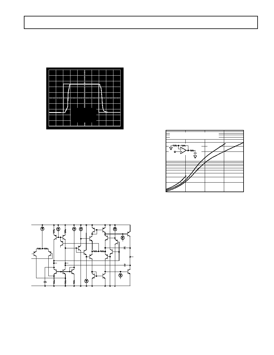
Overdrive Recovery
Overdrive of an amplifier occurs when the output and/or input
range are exceeded. The amplifier must recover from this over-
drive condition. As shown in Figure 33, the AD8042 recovers
within 30 ns from negative overdrive and within 25 ns from
positive overdrive.
+5V
+2.5V
0V
50ns
1V
V
S
= +5V
V
IN
= +5V p-p
G = +2
R
L
= 1k TO +2.5V
Figure 33. Overdrive Recovery
Circuit Description
The AD8042 is fabricated on Analog Devices' proprietary
eXtra-Fast Complementary Bipolar (XFCB) process which
enables the construction of PNP and NPN transistors with
similar f
T
s in the 2 GHz4 GHz region. The process is dielectri-
cally isolated to eliminate the parasitic and latch-up problems
caused by junction isolation. These features allow the construc-
tion of high frequency, low distortion amplifiers with low supply
currents. This design uses a differential output input stage to
maximize bandwidth and headroom (see Figure 34). The
smaller signal swings required on the first stage outputs (nodes
S1P, S1N) reduce the effect of nonlinear currents due to
junction capacitances and improve the distortion performance.
With this design harmonic distortion of better than 77 dB
@ 1 MHz into 100
with V
OUT
= 2 V p-p (Gain = +2) on a
single 5 volt supply is achieved.
SIN
R21
R3
V
EE
Q11
Q3
I10
R26
R39
Q5
Q4
Q40
I7
R2
R15
Q13
Q17
R5
C7
Q2
SIP
Q22
Q7
Q21
Q24
R23 R27
I2
I 3
I1
Q51
Q25
Q50
Q39
Q47
Q27
Q31
Q23
I9
I5
V
EE
V
CC
I8
Q36
Q8
V
OUT
C3
C9
V
CC
V
IN
P
V
IN
N
V
EE
Figure 34. AD8042 Simplified Schematic
The AD8042's rail-to-rail output range is provided by a
complementary common-emitter output stage. High output
drive capability is provided by injecting all output stage
predriver currents directly into the bases of the output devices
Q8 and Q36. Biasing of Q8 and Q36 is accomplished by I8 and
I5, along with a common-mode feedback loop (not shown).
This circuit topology allows the AD8042 to drive 40 mA of
output current with the outputs within 0.5 V of the supply rails.
On the input side, the device can handle voltages from 0.2 V
below the negative rail to within 1.2 V of the positive rail. Ex-
ceeding these values will not cause phase reversal; however, the
input ESD devices will begin to conduct if the input voltages
exceed the rails by greater than 0.5 V.
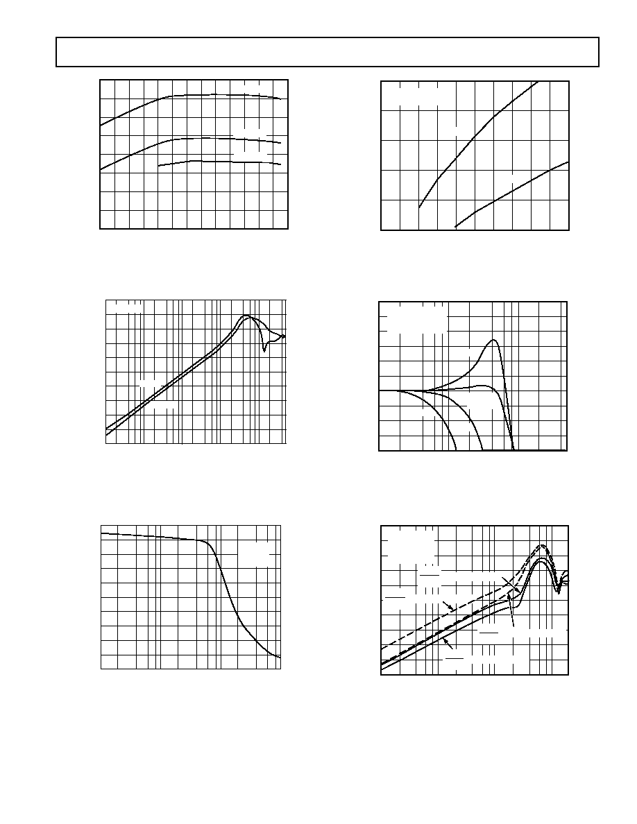
DRIVING CAPACITIVE LOADS
The capacitive load drive of the AD8042 can be increased by
adding a low valued resistor in series with the load. Figure 35
shows the effects of a series resistor on capacitive drive for vary-
ing voltage gains. As the closed-loop gain is increased, the larger
phase margin allows for larger capacitive loads with less over-
shoot. Adding a series resistor with lower closed-loop gains
accomplishes this same effect. For large capacitive loads, the
frequency response of the amplifier will be dominated by the
roll-off of the series resistor and capacitive load.
1000
10
100
1
2
5
CAPACITIVE LOAD pF
CLOSED-LOOP GAIN V/V
3
4
R
S
C
L
V
S
= +5V
200mV STEP WITH 30% OVERSHOOT
R
S
= 20
R
S
= 5
R
S
= 0
Figure 35. Capacitive Load Drive vs. Closed-Loop Gain
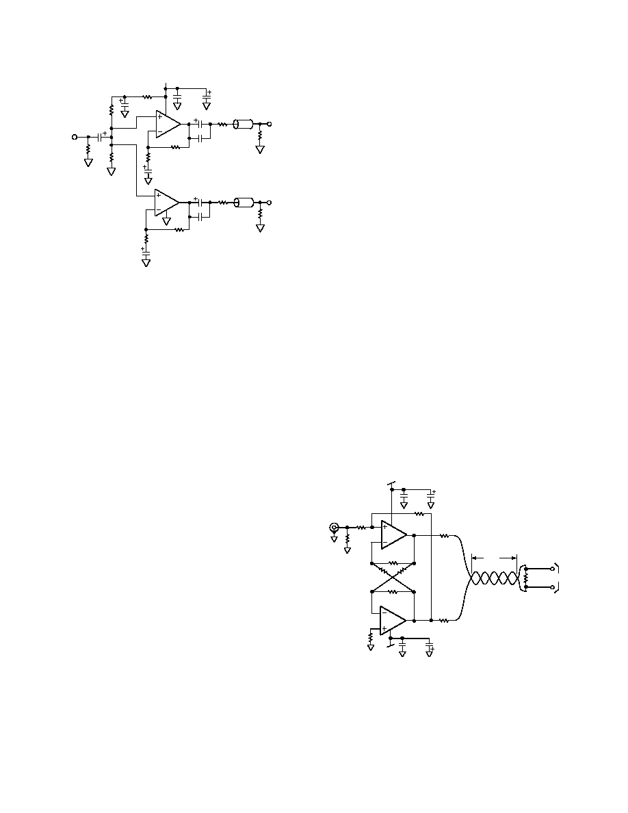
Single Supply Composite Video Line Driver
The two op amps of an AD8042 can be configured as a single
supply dual line driver for composite video. The wide signal
swing of the AD8042 enables this function to be performed
without using any type of clamping or dc restore circuit which
can cause signal distortion.
Figure 36 shows a schematic for a circuit that is driven by a
single composite video source that is ac coupled, level shifted
and applied to both + inputs of the two amplifiers. Each op amp
provides a separate 75
composite video output. To obtain
single supply operation, ac coupling is used throughout. The
large capacitor values are required to ensure that there is mini-
mal tilting of the video signals due to their low frequency
(30 Hz) signal content. The circuit shown was measured to have
a differential gain of 0.06% and a differential phase of 0.06
°
.
The input is terminated in 75
and ac coupled via C
IN
to a
voltage divider that provides the dc bias point to the input.
Setting the optimal bias point requires some understanding of
the nature of composite video signals and the video performance
of the AD8042.
AD8042
REV. A
12
+5V
0.1µF
10 F
8
3
2
R
F
1000 F
0.1 F
R
T
75
COAX
75
R
L
75
V
OUT
R
G
1k
R
T
75
V
OUT
1000 F
0.1 F
4
6
5
1
7
R
F
1k
R
G
1k
220 F
220 F
10 F
4.99k
4.99k
75
10k
COMPOSITE
VIDEO
IN
1k
R
L
75
Figure 36. Single Supply Composite Video Line Driver
Using AD8042
Signals of bounded peak-to-peak amplitude that vary in duty
cycle require larger dynamic swing capability than their peak-to-
peak amplitude after ac coupling. As a worst case, the dynamic
signal swing required will approach twice the peak-to-peak
value. The two bounding cases are for a duty cycle that is mostly
low, but occasionally goes high at a fraction of a percent duty
cycle and vice versa.
Composite video is not quite this demanding. One bounding
extreme is for a signal that is mostly black for an entire frame,
but has a white (full intensity), minimum width spike at least
once per frame.
The other extreme is for a video signal that is full white every-
where. The blanking intervals and sync tips of such a signal will
have negative going excursions in compliance with composite
video specifications. The combination of horizontal and vertical
blanking intervals limit such a signal to being at its highest level
(white) for only about 75% of the time.
As a result of the duty cycle variations between the two extremes
presented above, a 1 V p-p composite video signal that is multi-
plied by a gain of two requires about 3.2 V p-p of dynamic volt-
age swing at the output for an op amp to pass a composite video
signal of arbitrary duty cycle without distortion.
Some circuits use a sync tip clamp along with ac coupling to
hold the sync tips at a relatively constant level in order to lower
the amount of dynamic signal swing required. However, these
circuits can have artifacts like sync tip compression unless they
are driven by sources with very low output impedance.
The AD8042 not only has ample signal swing capability to
handle the dynamic range required without using a sync tip
clamp, but also has good video specifications like differential
gain and differential phase when buffering these signals in an
ac-coupled configuration.
To test this, the differential gain and differential phase were
measured for the AD8042 while the supplies were varied. As the
lower supply is raised to approach the video signal, the first
effect to be observed is that the sync tips become compressed
before the differential gain and differential phase are adversely
affected. Thus, there must be adequate swing in the negative
direction to pass the sync tips without compression.
As the upper supply is lowered to approach the video, the differ-
ential gain and differential phase were not significantly adversely
affected until the difference between the peak video output and
the supply reached 0.6 V. Thus, the highest video level should
be kept at least 0.6 V below the positive supply rail.
Taking the above into account, it was found that the optimal
point to bias the noninverting input is at 2.2 V dc. Operating at
this point, the worst case differential gain is measured at 0.06%
and the worst case differential phase is 0.06
°
.
The ac coupling capacitors used in the circuit at first glance
appear quite large. A composite video signal has a lower fre-
quency band edge of 30 Hz. The resistances at the various ac
coupling points--especially at the output--are quite small. In
order to minimize phase shifts and baseline tilt, the large value
capacitors are required. For video system performance that is
not to be of the highest quality, the value of these capacitors can
be reduced by a factor of up to five with only a slightly observ-
able change in the picture quality.
Single-Ended-to-Differential Driver
Using a cross-coupled single-ended-to-differential converter, the
AD8042 makes a good general purpose differential line driver.
This can be used for applications such as driving category 5
twisted pair wire which is becoming common for data communi-
cations in buildings. Figure 37 shows a configuration for a cir-
cuit that performs this function that can be used for video
transmission over a differential pair or various data communica-
tion purposes.
50m
AMP1
8
3
2
6
5
7
4
5V
1
AD8042
100
0.1 F
10 F
60.4
60.4
1k
V
IN
49.9
R
IN
1k
R
A
R
A
1k
1k
1k
R
F
1k
121
R
B
R
B
0.1 F
10 F
V
OUT
AMP2
Figure 37. Single-Ended-to-Differential Twisted Pair Line
Driver
AD8042
REV. A
13
Each of the AD8042's op amps is configured as a unity gain
follower by the feedback resistors (R
A
). Each op amp output
also drives the other as a unity gain inverter via the two R
B
s,
creating a totally symmetrical circuit.
If the + input to Amp 2 is grounded and a small positive signal
is applied to the + input of Amp 1, the output of Amp 1 will be
driven to saturation in the positive direction and the input of
Amp 2 driven to saturation in the negative direction. This is
similar to the way a conventional op amp behaves without any
feedback.
If a resistor (R
F
) is connected from the output of Amp 2 to the
+ input of Amp 1, negative feedback is provided which closes
the loop. An input resistor (R
I
) will make the circuit look like a
conventional inverting op amp configuration with differential
outputs.
The gain of this circuit from input to either output will be
±
R
F
/
R
I
. Or the single-ended-to-differential gain will be 2
×
R
F
/R
I.
This gives the circuit the advantage of being able to adjust its
gain by changing a single resistor.
The cable has a characteristic impedance of about 120
. Each
driver output is back terminated with a pair of 60.4
resistors
to make the source look like 120
. The receive end is termi-
nated with 121
, and the signal is measured differentially with
a pair of scope probes. One channel on the oscilloscope is in-
verted and then the signals are added.
The scope photo in Figure 38 shows a 10 MHz, 2 V p-p input
signal driving the circuit with 50 m of category 5 twisted pair
wire.
10
0%
100
90
50ns
200mV
1V
200mV
V
IN
V
OUT
Figure 38. Differential Driver Frequency Response
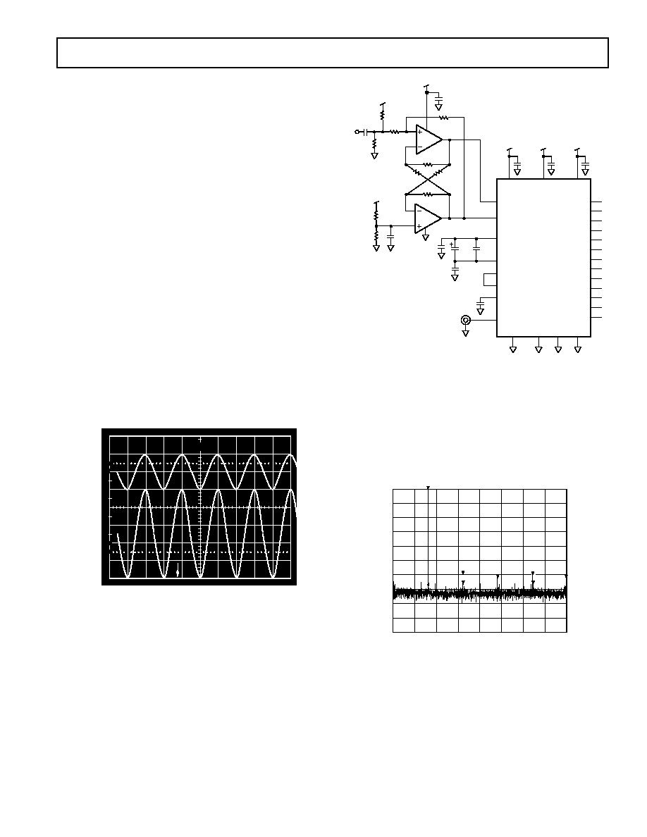
Single Supply Differential A/D Driver
The single-ended-to-differential converter circuit is also useful
as a differential driver for video speed, single-ended, differential
input A/D converters. Figure 39 is a schematic that shows such
a circuit differentially driving an AD9220, a 12-bit, 10 MSPS
A/D converter.
AD9220
V
IN
A
V
IN
B
CAPT
CAPB
V
REF
SENSE
CML
CLK
19
27
25
14
13
12
11
10
9
8
7
6
5
4
3
2
+5V
0.1 F
DV
DD
AV
DD
AV
DD
REFCOM
DV
SS
AV
SS
AV
SS
16
28
15
26
OTR
BIT1
BIT2
BIT3
BIT4
BIT5
BIT6
BIT7
BIT8
BIT9
BIT10
BIT11
BIT12
CLOCK
1
0.1 F
0.1 F
18
17
22
10/16
8
3
2
6
5
7
4
+5V
1
AD8042
2.49k
0.1 F
1k
V
IN
1k
1k
1k
1k
1k
0.1 F
+5V
+5V
0.1 F
2.49k
0.1 F
0.1 F
+5V
0.1 F
+5V
0.1 F
Figure 39. AD8042 Differential Driver for the AD9220
12-Bit, 10 MSPS A/D Converter
The circuit was tested with a 1 MHz input signal and clocked at
10 MHz. An FFT response of the digital output is shown in
Figure 40.
Pin 5 is biased at 2.5 V by the voltage divider and bypassed.
This biases each output at 2.5 V. V
IN
is ac coupled such that V
IN
going positive makes V
IN
A go positive and V
IN
B go in the nega-
tive direction. The opposite happens for a negative going V
IN
.
VERTICAL SCALE 15dB/DIV
1
4
9
7
2
3
6
8
5
FUND FRQ 1000977
SMPL FRQ 10000000
THD 82.00
SNR 71.13
SINAD 70.79
SFDR 86.74
2nd 88.34
3rd 86.74
4th 99.26
5th 90.67
6th 99.47
7th 91.16
8th 97.25
9th 91.61
HARMONICS (dBc)
Figure 40. FFT of AD9220 Output When Driven by AD8042
AD8042
REV. A
14
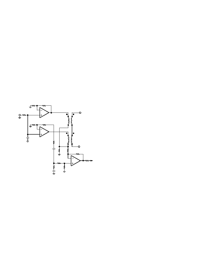
HDSL Line Driver
HDSL or high-bit-rate digital subscriber line is becoming popu-
lar as a means to provide data communication at DS1 rates
(1.544 MBPS) over moderate distances via conventional tele-
phone twisted pair wires. In these systems, the transceiver at the
customer's end is sometimes powered via the twisted pair from a
power source at the central office. It is sometimes required to
raise the dc voltage of the power source to compensate for IR
drops in long lines or lines with narrow gauge wires.
Because of this, it is highly desirable to keep the power con-
sumption of the customer's transceiver as low as possible. One
means to realize significant power savings is to run the trans-
ceiver from a
±
5 V supply instead of the more conventional
±
12 V.
The high output swing and current drive capability of the
AD8042 make it ideally suited to this application. Figure 41
shows a circuit for the analog portion of an HDSL transceiver
using the AD8042 as the line driver.
2k
3k
232
V
IN
0.001 F
V
OUT
6
5
7
1
4
10
5
ATT
2718AF
93DJ39
34
2k
2k
249
2k
2k
2k
0.001 F
2
3
1
V
REC
1/2
AD8042
2k
3k
2
3
1
1/2
AD8042
912
0.0027 F
2
7
9
6
1/4
AD8044
Figure 41. HDSL Line Driver
Layout Considerations
The specified high speed performance of the AD8042 requires
careful attention to board layout and component selection.
Proper RF design techniques and low-pass parasitic component
selection are necessary.
The PCB should have a ground plane covering all unused por-
tions of the component side of the board to provide a low im-
pedance path. The ground plane should be removed from the
area near the input pins to reduce the stray capacitance.
Chip capacitors should be used for the supply bypassing.
One end should be connected to the ground plane and the
other within 1/8 inch of each power pin. An additional large
(0.47
µ
F10
µ
F) tantalum electrolytic capacitor should be con-
nected in parallel, but not necessarily so close, to supply current
for fast, large signal changes at the output.
The feedback resistor should be located close to the inverting
input pin in order to keep the stray capacitance at this node to a
minimum. Capacitance variations of less than 1 pF at the in-
verting input will significantly affect high speed performance.
Stripline design techniques should be used for long signal traces
(greater than about 1 inch). These should be designed with a
characteristic impedance of 50
or 75
and be properly termi-
nated at each end.
AD8042
REV. A
15
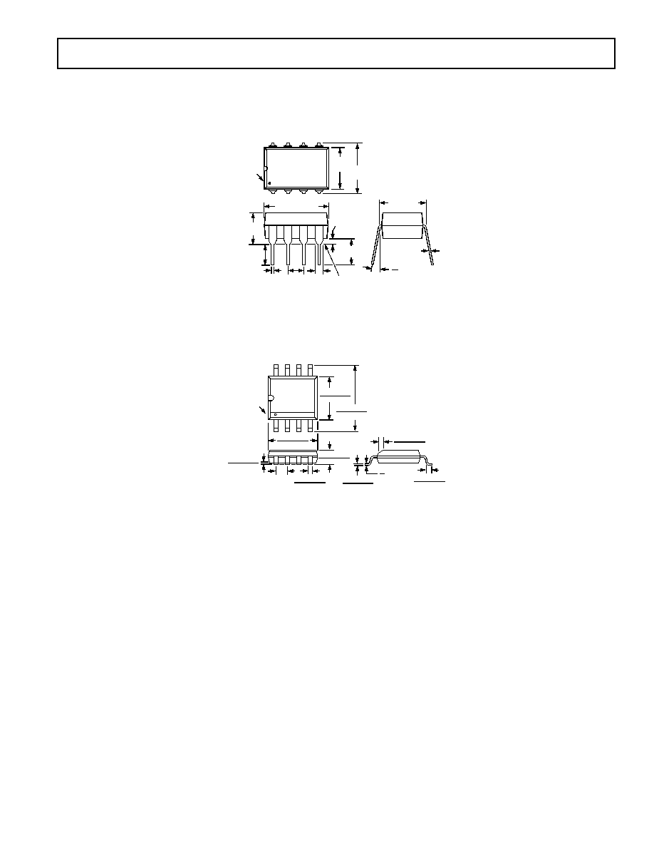
OUTLINE DIMENSIONS
Dimensions shown in inches and (mm).
8-Lead Plastic DIP
(N-8)
0.011±0.003
(0.28±0.08)
0.30 (7.62)
REF
15
°
0
°
PIN 1
4
5
8
1
0.25
(6.35)
0.31
(7.87)
0.10
(2.54)
BSC
SEATING
PLANE
0.035±0.01
(0.89±0.25)
0.18±0.03
(4.57±0.76)
0.033
(0.84)
NOM
0.018±0.003
(0.46±0.08)
0.125
(3.18)
MIN
0.165±0.01
(4.19±0.25)
0.39 (9.91) MAX
8-Lead Plastic SOIC
(SO-8)
0.0098 (0.25)
0.0075 (0.19)
0.0500 (1.27)
0.0160 (0.41)
8
°
0
°
0.0196 (0.50)
0.0099 (0.25)
x 45
°
PIN 1
0.1574 (4.00)
0.1497 (3.80)
0.2440 (6.20)
0.2284 (5.80)
4
5
1
8
0.0192 (0.49)
0.0138 (0.35)
0.0500
(1.27)
BSC
0.0688 (1.75)
0.0532 (1.35)
0.0098 (0.25)
0.0040 (0.10)
0.1968 (5.00)
0.1890 (4.80)
PRINTED IN U.S.A.
C2082a09/99