 | ÐлекÑÑоннÑй компоненÑ: AD8048 | СкаÑаÑÑ:  PDF PDF  ZIP ZIP |
Äîêóìåíòàöèÿ è îïèñàíèÿ www.docs.chipfind.ru
REV. 0
Information furnished by Analog Devices is believed to be accurate and
reliable. However, no responsibility is assumed by Analog Devices for its
use, nor for any infringements of patents or other rights of third parties
which may result from its use. No license is granted by implication or
otherwise under any patent or patent rights of Analog Devices.
a
250 MHz, General Purpose
Voltage Feedback Op Amps
AD8047/AD8048
The AD8047 and AD8048's low distortion and cap load drive
make the AD8047/AD8048 ideal for buffering high speed
ADCs. They are suitable for 12 bit/10 MSPS or 8 bit/60 MSPS
ADCs. Additionally, the balanced high impedance inputs of the
voltage feedback architecture allow maximum flexibility when
designing active filters.
The AD8047 and AD8048 are offered in industrial (40
°
C to
+85
°
C) temperature ranges and are available in 8-pin plastic
DIP and SOIC packages.
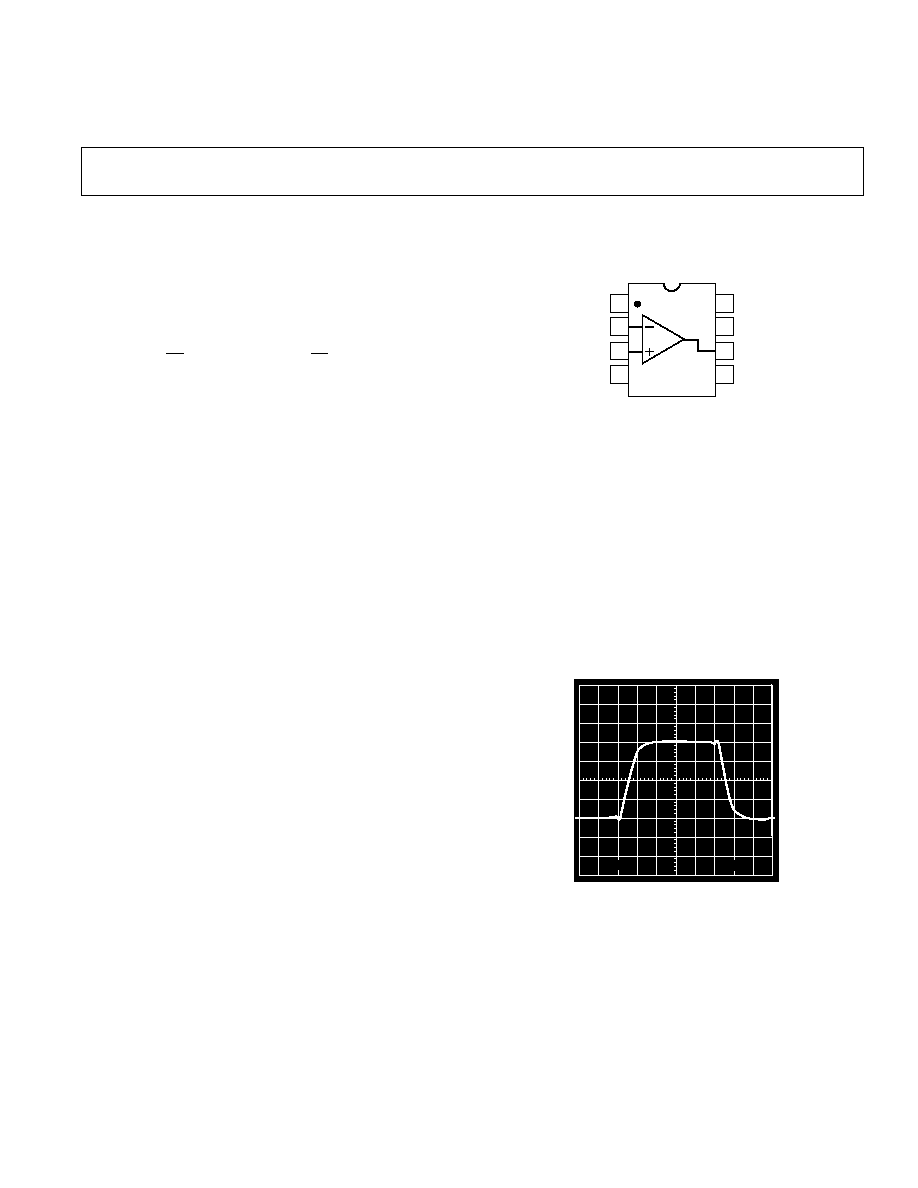
5ns
1V
Figure 1. AD8047 Large Signal Transient Response,
V
O
= 4 V p-p, G = +1
FEATURES
Wide Bandwidth
AD8047, G = +1 AD8048, G = +2
Small Signal
250 MHz
260 MHz
Large Signal (2 V p-p)
130 MHz
160 MHz
5.8 mA Typical Supply Current
Low Distortion, (SFDR) Low Noise
66 dBc typ @ 5 MHz
54 dBc typ @ 20 MHz
5.2 nV/
Hz (AD8047), 3.8 nV/
Hz (AD8048) Noise
Drives 50 pF Capacitive Load
High Speed
Slew Rate 750 V/
µ
s (AD8047), 1000 V/
µ
s (AD8048)
Settling 30 ns to 0.01%, 2 V Step
±
3 V to
±
6 V Supply Operation
APPLICATIONS
Low Power ADC Input Driver
Differential Amplifiers
IF/RF Amplifiers
Pulse Amplifiers
Professional Video
DAC Current to Voltage Conversion
Baseband and Video Communications
Pin Diode Receivers
Active Filters/Integrators
PRODUCT DESCRIPTION
The AD8047 and AD8048 are very high speed and wide band-
width amplifiers. The AD8047 is unity gain stable. The
AD8048 is stable at gains of two or greater. The AD8047 and
AD8048, which utilize a voltage feedback architecture, meet the
requirements of many applications that previously depended on
current feedback amplifiers.
A proprietary circuit has produced an amplifier that combines
many of the best characteristics of both current feedback and
voltage feedback amplifiers. For the power (6.6 mA max) the
AD8047 and AD8048 exhibit fast and accurate pulse response
(30 ns to 0.01%) as well as extremely wide small signal and
large signal bandwidth and low distortion. The AD8047
achieves 54 dBc distortion at 20 MHz and 250 MHz small sig-
nal and 130 MHz large signal bandwidths.
FUNCTIONAL BLOCK DIAGRAM
8-Pin Plastic Mini-DIP (N), Cerdip (Q)
and SO (R) Packages
1
2
3
4
8
7
6
5
AD8047/48
NC
INPUT
+INPUT
V
S
NC
+V
S
OUTPUT
NC
(Top View)
NC = NO CONNECT
© Analog Devices, Inc., 1995
One Technology Way, P.O. Box 9106, Norwood. MA 02062-9106, U.S.A.
Tel: 617/329-4700
Fax: 617/326-8703

AD8047A
AD8048A
Parameter
Conditions
Min
Typ Max
Min
Typ Max
Units
DYNAMIC PERFORMANCE
Bandwidth (3 dB)
Small Signal
V
OUT
0.4 V p-p
170
250
180
260
MHz
Large Signal
1
V
OUT
= 2 V p-p
100
130
135
160
MHz
Bandwidth for 0.1 dB Flatness
V
OUT
= 300 mV p-p
8047, R
F
= 0
; 8048, R
F
= 200
35
50
MHz
Slew Rate, Average +/
V
OUT
= 4 V Step
475
750
740
1000
V/
µ
s
Rise/Fall Time
V
OUT
= 0.5 V Step
1.1
1.2
ns
V
OUT
= 4 V Step
4.3
3.2
ns
Settling Time
To 0.1%
V
OUT
= 2 V Step
13
13
ns
To 0.01%
V
OUT
= 2 V Step
30
30
ns
HARMONIC/NOISE PERFORMANCE
2nd Harmonic Distortion
2 V p-p; 20 MHz
54
48
dBc
R
L
= 1 k
64
60
dBc
3rd Harmonic Distortion
2 V p-p; 20 MHz
60
56
dBc
R
L
= 1 k
61
65
dBc
Input Voltage Noise
f = 100 kHz
5.2
3.8
nV/
Hz
Input Current Noise
f = 100 kHz
1.0
1.0
pA/
Hz
Average Equivalent Integrated
Input Noise Voltage
0.1 MHz to 10 MHz
16
11
µ
V rms
Differential Gain Error (3.58 MHz)
R
L
= 150
, G = +2
0.02
0.01
%
Differential Phase Error (3.58 MHz)
R
L
= 150
, G = +2
0.03
0.02
Degree
DC PERFORMANCE
2
,
R
L
= 150
Input Offset Voltage
3
1
3
1
3
mV
T
MIN
T
MAX
4
4
mV
Offset Voltage Drift
±
5
±
5
µ
V/
°
C
Input Bias Current
1
3.5
1
3.5
µ
A
T
MIN
T
MAX
6.5
6.5
µ
A
Input Offset Current
0.5
2
0.5
2
µ
A
T
MIN
T
MAX
3
3
µ
A
Common-Mode Rejection Ratio
V
CM
=
±
2.5 V
74
80
74
80
dB
Open-Loop Gain
V
OUT
=
±
2.5 V
58
62
65
68
dB
T
MIN
T
MAX
54
56
dB
INPUT CHARACTERISTICS
Input Resistance
500
500
k
Input Capacitance
1.5
1.5
pF
Input Common-Mode Voltage Range
±
3.4
±
3.4
V
OUTPUT CHARACTERISTICS
Output Voltage Range, R
L
= 150
±
2.8
±
3.0
±
2.8
±
3.0
V
Output Current
50
50
mA
Output Resistance
0.2
0.2
Short Circuit Current
130
130
mA
POWER SUPPLY
Operating Range
±
3.0
±
5.0
±
6.0
±
3.0
±
5.0
±
6.0
V
Quiescent Current
5.8
6.6
5.9
6.6
mA
T
MIN
T
MAX
7.5
7.5
mA
Power Supply Rejection Ratio
72
78
72
78
dB
NOTES
1
See Max Ratings and Theory of Operation sections of data sheet.
2
Measured at A
V
= 50.
3
Measured with respect to the inverting input.
Specifications subject to change without notice.
(
±
V
S
=
±
5 V; R
LOAD
= 100
; A
V
= 1 (AD8047); A
V
= 2 (AD8048), unless otherwise noted)
AD8047/AD8048SPECIFICATIONS
ELECTRICAL CHARACTERISTICS
REV. 0
2
AD8047/AD8048
REV. 0
3
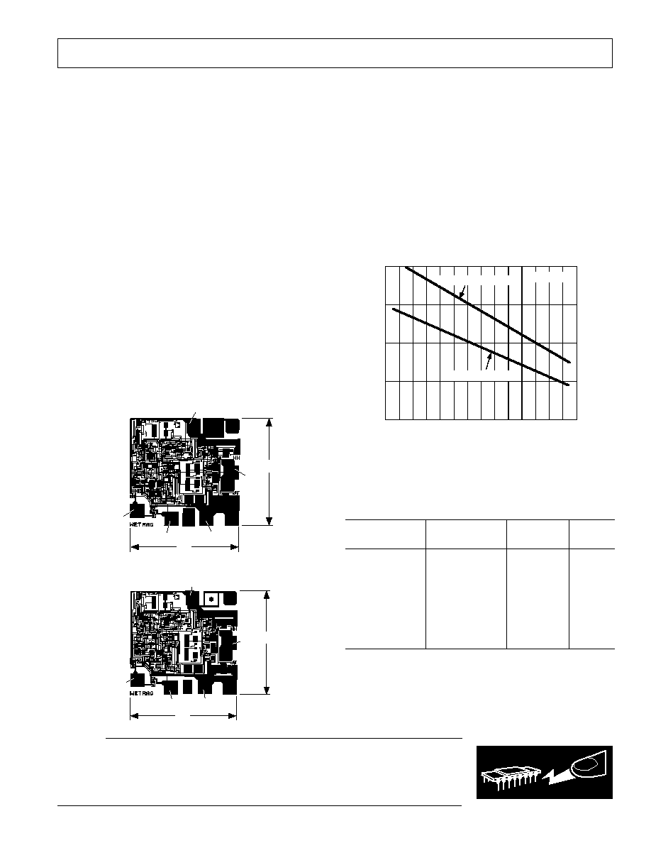
MAXIMUM POWER DISSIPATION
The maximum power that can be safely dissipated by these de-
vices is limited by the associated rise in junction temperature.
The maximum safe junction temperature for plastic encapsu-
lated devices is determined by the glass transition temperature
of the plastic, approximately +150
°
C. Exceeding this limit tem-
porarily may cause a shift in parametric performance due to a
change in the stresses exerted on the die by the package. Exceed-
ing a junction temperature of +175
°
C for an extended period can
result in device failure.
While the AD8047 and AD8048 are internally short circuit pro-
tected, this may not be sufficient to guarantee that the maxi-
mum junction temperature (+150
°
C) is not exceeded under all
conditions. To ensure proper operation, it is necessary to ob-
serve the maximum power derating curves.
2.0
0
50 80
1.5
0.5
40
1.0
0
10
10
20
30
20 30 40 50 60 70
90
AMBIENT TEMPERATURE
°
C
MAXIMUM POWER DISSIPATION Watts
T
J
= +150
°
C
8-PIN MINI-DIP PACKAGE
8-PIN SOIC PACKAGE
Figure 2. Plot of Maximum Power Dissipation vs.
Temperature
ORDERING GUIDE
Temperature
Package
Package
Model
Range
Description Option*
AD8047AN
40
°
C to +85
°
C
Plastic DIP
N-8
AD8047AR
40
°
C to +85
°
C
SOIC
R-8
AD8047-EB
Evaluation
Board
AD8048AN
40
°
C to +85
°
C
Plastic DIP
N-8
AD8048AR
40
°
C to +85
°
C
SOIC
R-8
AD8048-EB
Evaluation
Board
*N = Plastic DIP; R= SOIC (Small Outline Integrated Circuit)
ABSOLUTE MAXIMUM RATINGS
1
Supply Voltage . . . . . . . . . . . . . . . . . . . . . . . . . . . . . . . . 12.6 V
Voltage Swing
×
Bandwidth Product (AD8047) . . . 180 V MHz
(AD8048) . . . 250 V
MHz
Internal Power Dissipation
2
Plastic Package (N) . . . . . . . . . . . . . . . . . . . . . . . . 1.3 Watts
Small Outline Package (R) . . . . . . . . . . . . . . . . . . . 0.9 Watts
Input Voltage (Common Mode) . . . . . . . . . . . . . . . . . . . .
±
V
S
Differential Input Voltage . . . . . . . . . . . . . . . . . . . . . . .
±
1.2 V
Output Short Circuit Duration
. . . . . . . . . . . . . . . . . . . . . . Observe Power Derating Curves
Storage Temperature Range (N, R) . . . . . . . . 65
°
C to +125
°
C
Operating Temperature Range (A Grade) . . . 40
°
C to +85
°
C
Lead Temperature Range (Soldering 10 sec) . . . . . . . . +300
°
C
NOTES
1
Stresses above those listed under "Absolute Maximum Ratings" may cause
permanent damage to the device. This is a stress rating only, and functional
operation of the device at these or any other conditions above those indicated in the
operational section of this specification is not implied. Exposure to absolute
maximum rating conditions for extended periods may affect device reliability.
2
Specification is for device in free air:
8-Pin Plastic DIP Package:
JA
= 90
°
C/Watt
8-Pin SOIC Package:
JA
= 140
°
C/Watt
WARNING!
ESD SENSITIVE DEVICE
CAUTION
ESD (electrostatic discharge) sensitive device. Electrostatic charges as high as 4000 V readily
accumulate on the human body and test equipment and can discharge without detection.
Although these devices feature proprietary ESD protection circuitry, permanent damage may
occur on devices subjected to high energy electrostatic discharges. Therefore, proper ESD
precautions are recommended to avoid performance degradation or loss of functionality.
METALIZATION PHOTOS
Dimensions shown in inches and (mm).
Connect Substrate to V
S
.
AD8047
+V
S
V
OUT
V
S
IN
+IN
0.045
(1.14)
0.044
(1.13)
AD8048
+V
S
V
S
OUT
IN
+IN
0.045
(1.14)
0.044
(1.13)
REV. 0
4
AD8047/AD8048
AD8047Typical Characteristics
+V
S
PULSE
GENERATOR
R
L
= 100
V
S
V
IN
V
OUT
0.1
µ
F
10
µ
F
AD8047
3
2
7
6
0.1
µ
F
10
µ
F
4
T
R
/T
F
= 500ps
R
T
= 49.9
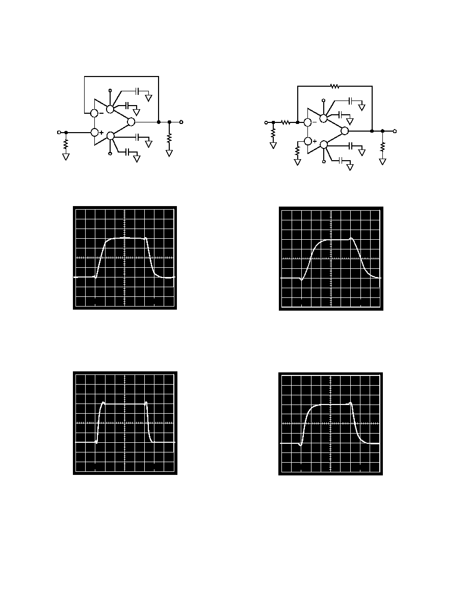
Figure 3. Noninverting Configuration, G = +1
5ns
1V
Figure 4. Large Signal Transient Response;
V
O
= 4 V p-p, G = +1
5ns
100mV
Figure 5. Small Signal Transient Response;
V
O
= 400 mV p-p, G = +1
100
+V
S
V
S
0.1
µ
F
10
µ
F
AD8047
3
2
7
6
0.1
µ
F
10
µ
F
4
R
IN
R
F
R
L
= 100
V
OUT
T
R
/T
F
= 500ps
PULSE
GENERATOR
V
IN
R
T
= 66.5
Figure 6. Inverting Configuration, G = 1
5ns
1V
Figure 7. Large Signal Transient Response;
V
O
= 4 V p-p, G = 1, R
F
= R
IN
= 200
5ns
100mV
Figure 8. Small Signal Transient Response;
V
O
= 400 mV p-p, G = 1, R
F
= R
IN
= 200
AD8047/AD8048
REV. 0
5
AD8048Typical Characteristics
PULSE
GENERATOR
R
F
+V
S
R
L
= 100
V
S
V
IN
V
OUT
0.1
µ
F
10
µ
F
AD8048
3
2
7
6
0.1
µ
F
10
µ
F
4
T
R
/T
F
= 500ps
R
IN
R
T
= 49.9
Figure 9. Noninverting Configuration, G = +2
5ns
1V
Figure 10. Large Signal Transient Response;
V
O
= 4 V p-p, G = +2, R
F
= R
IN
= 200
5ns
100mV
Figure 11. Small Signal Transient Response;
V
O
= 400 mV p-p, G = +2, R
F
= R
IN
= 200
R
S
= 100
R
F
+V
S
R
L
= 100
V
S
V
OUT
0.1
µ
F
10
µ
F
AD8048
3
2
7
6
0.1
µ
F
10
µ
F
4
T
R
/T
F
= 500ps
V
IN
PULSE
GENERATOR
R
T
= 66.5
R
IN
Figure 12. Inverting Configuration, G= 1
5ns
1V
Figure 13. Large Signal Transient Response;
V
O
= 4 V p-p, G = 1, R
F
=
R
IN
= 200
5ns
100mV
Figure 14. Small Signal Transient Response;
V
O
= 400 mV p-p, G = 1, R
F
= R
IN
= 200
REV. 0
6
AD8047/AD8048
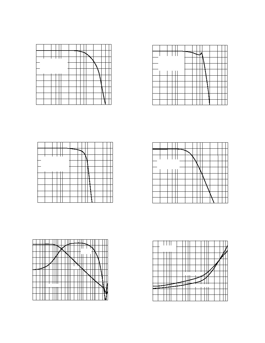
AD8047Typical Characteristics
6
8
4
2
0
FREQUENCY Hz
1G
100M
10M
R
L
= 100
R
F
= 0
FOR DIP
R
F
= 66.5
FOR SOIC
V
OUT
= 300mV p-p
1M
1
1
3
5
7
OUTPUT dBm
9
Figure 15. AD8047 Small Signal Frequency Response
G = +1
0.6
0.8
0.4
0.2
0
FREQUENCY Hz
1G
100M
10M
OUTPUT dBm
R
L
= 100
R
F
= 0
FOR DIP
R
F
= 66.5
FOR SOIC
V
OUT
= 300mV p-p
1M
0.1
0.1
0.3
0.5
0.7
0.9
Figure 16. AD8047 0.1 dB Flatness, G = +1
0
20
20
40
60
FREQUENCY Hz
1G
10M
10k
GAIN dB
1k
70
50
30
10
10
30
40
80
0
40
80
100
60
20
20
60
100
PHASE MARGIN Degrees
PHASE
MARGIN
GAIN
100k
1M
100M
R
L
= 100
Figure 17. AD8047 Open-Loop Gain and Phase Margin vs.
Frequency
6
8
4
2
0
FREQUENCY Hz
1G
100M
10M
1M
1
1
3
5
7
9
OUTPUT dBm
R
L
= 100
R
F
= 0
FOR DIP
R
F
= 66.5
FOR SOIC
V
OUT
= 2V p-p
Figure 18. AD8047 Large Signal Frequency Response,
G = +1
6
8
4
2
0
FREQUENCY Hz
1G
100M
10M
1M
1
1
3
5
7
9
OUTPUT dBm
R
L
= 100
R
F
= R
IN
= 200
V
OUT
= 300mV p-p
Figure 19. AD8047 Small Signal Frequency Response,
G = 1
90
110
70
50
30
FREQUENCY Hz
100M
1M
100k
10k
40
20
60
80
100
120
OUTPUT dBm
10M
2ND HARMONIC
3RD HARMONIC
R
L
= 1k
V
OUT
= 2V p-p
Figure 20. AD8047 Harmonic Distortion vs. Frequency,
G = +1
AD8047/AD8048
REV. 0
7
90
110
70
50
30
FREQUENCY Hz
100M
1M
100k
10k
40
20
60
80
100
120
10M
2ND HARMONIC
3RD HARMONIC
R
L
= 100
V
OUT
= 2V p-p
HARMONIC DISTORTION dBc
Figure 21. AD8047 Harmonic Distortion vs. Frequency,
G = +1
OUTPUT SWING V p-p
25
30
HARMONIC DISTORTION dBc
65
1.6
6.5
2.5
3.5
4.5
5.5
45
50
55
60
35
40
2ND HARMONIC
3RD HARMONIC
f = 20MHz
R
L
= 1k
R
F
= 0
Figure 22. AD8047 Harmonic Distortion vs. Output Swing,
G = +1
0.04
DIFF GAIN %
0.04
0.00
0.02
0.02
11th
1st
2nd
3rd
4th
5th
6th
7th
8th
9th
10th
11th
1st
2nd
3rd
4th
5th
6th
7th
8th
9th
10th
0.04
DIFF PHASE Degrees 0.04
0.00
0.02
0.02
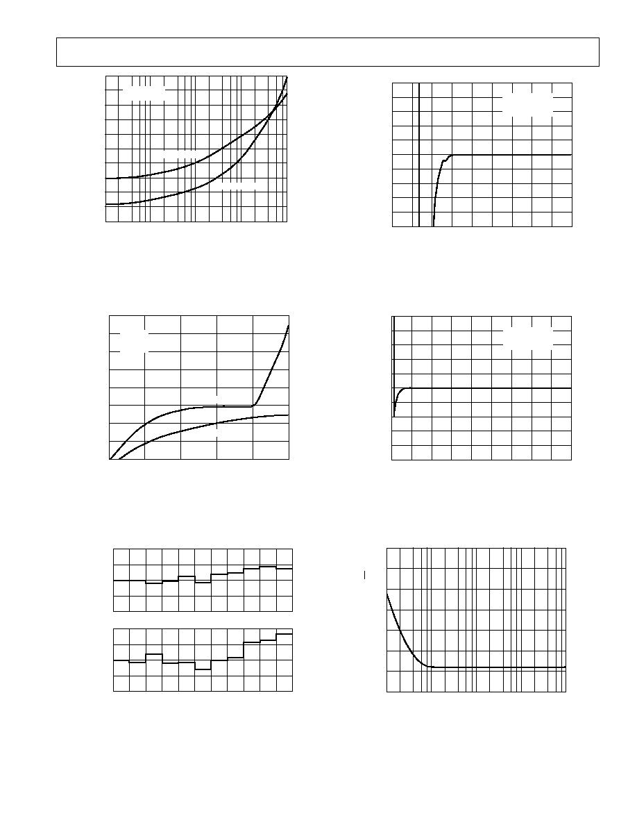
Figure 23. AD8047 Differential Gain and Phase Error,
G = +2, R
L
= 150
, R
F
= 200
, R
IN
= 200
SETTLING TIME ns
0.5
0.4
0.4
0
10
ERROR %
20
0.0
0.1
0.2
0.3
0.2
0.1
0.3
0.5
5
15
25
35
45
30
40
R
L
= 100
R
F
= 0
V
OUT
= 2V STEP
Figure 24. AD8047 Short-Term Settling Time, G = +1
SETTLING TIME µs
0.25
0.20
0.20
0
4
ERROR %
8
0.00
0.05
0.10
0.15
0.10
0.05
0.15
0.25
2
6
10
14
18
12
16
R
L
= 100
R
F
= 0
V
OUT
= 2V STEP
Figure 25. AD8047 Long-Term Settling Time, G = +1
17
13
3
100
100k
10k
1k
10
15
9
11
5
7
FREQUENCY Hz
INPUT NOISE VOLTAGE nV/
Hz
Figure 26. AD8047 Noise vs. Frequency
REV. 0
8
AD8047/AD8048
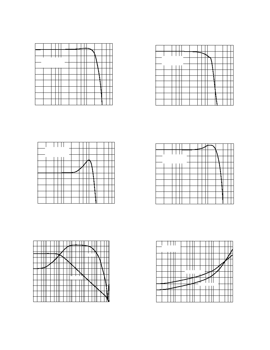
AD8048Typical Characteristics
3
10M
1G
100M
1M
5
1
3
1
FREQUENCY Hz
OUTPUT dBm
6
4
0
2
2
R
L
= 100
R
F
= R
IN
= 200
V
OUT
= 2V p-p
7
Figure 30. AD8048 Large Signal Frequency Response,
G = +2
9
10M
1G
100M
1M
1
5
3
7
FREQUENCY Hz
0
2
6
4
8
R
L
= 100
R
F
= R
IN
= 200
V
OUT
= 300mV p-p
OUTPUT dBm
1
Figure 31. AD8048 Small Signal Frequency Response,
G = 1
HARMONIC DISTORTION dBc
90
110
70
50
30
FREQUENCY Hz
100M
1M
100k
10k
40
20
60
80
100
120
10M
2ND HARMONIC
3RD HARMONIC
R
L
= 1k
V
OUT
= 2V p-p
Figure 32. AD8048 Harmonic Distortion vs. Frequency,
G = +2
Figure 27. AD8048 Small Signal Frequency Response,
G = +2
6.5
5.5
10M
1G
100M
1M
6.3
5.9
6.1
5.7
FREQUENCY Hz
OUTPUT dBm
6.4
6.2
5.8
6.0
5.6
R
L
= 100
R
F
= R
IN
= 200
V
OUT
= 300mV p-p
Figure 28. AD8048 0.1 dB Flatness, G = +2
70
20
10k
100k
1G
100M
10M
1M
FREQUENCY Hz
60
20
30
40
50
10
0
10
GAIN dB
40
120
20
0
20
100
80
60
PHASE Degrees
R
L
= 100
PHASE
1k
40
60
80
100
80
90
Figure 29. AD8048 Open-Loop Gain and Phase Margin vs.
Frequency
7
3
10M
1G
100M
1M
5
1
3
1
FREQUENCY Hz
OUTPUT dBm
6
4
0
2
2
R
L
= 100
R
F
= R
IN
= 200
V
OUT
= 300mV p-p
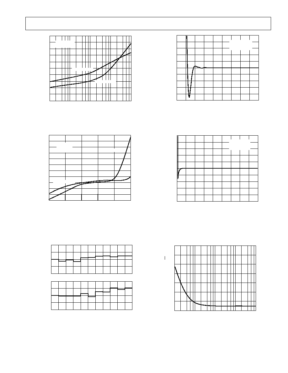
AD8047/AD8048
REV. 0
9
SETTLING TIME ns
0.5
0.4
0.4
0
10
ERROR %
20
0.0
0.1
0.2
0.3
0.2
0.1
0.3
0.5
5
15
25
35
45
30
40
R
L
= 100
R
F
= 200
V
OUT
= 2V STEP
Figure 36. AD8048 Short-Term Settling Time, G = +2
SETTLING TIME µs
0.25
0.20
0.20
0
4
ERROR %
8
0.0
0.05
0.10
0.15
0.10
0.05
0.15
0.25
2
6
10
14
18
12
16
R
L
= 100
R
F
= 200
V
OUT
= 2V STEP
Figure 37. AD8048 Long-Term Settling Time 2 V Step,
G = +2
17
13
3
100
100k
10k
1k
10
15
9
11
5
7
FREQUENCY Hz
INPUT NOISE VOLTAGE nV/
Hz
Figure 38. AD8048 Noise vs. Frequency
OUTPUT SWING Volts p-p
15
70
1.5
5.5
2.5
3.5
4.5
6.5
HARMONIC DISTORTION dBc
55
65
25
35
45
f = 20MHz
R
L
= 1k
R
F
= 200
2ND HARMONIC
3RD HARMONIC
20
60
30
40
50
Figure 34. AD8048 Harmonic Distortion vs. Output Swing,
G = +2
0.04
DIFF GAIN %
0.04
0.00
0.02
0.02
11th
1st
2nd
3rd
4th
5th
6th
7th
8th
9th
10th
11th
1st
2nd
3rd
4th
5th
6th
7th
8th
9th
10th
0.04
DIFF PHASE Degrees 0.04
0.00
0.02
0.02
Figure 35. AD8048 Differential Gain and Phase Error,
G = +2, R
L
= 150
, R
F
= 200
, R
IN
= 200
Figure 33. AD8048 Harmonic Distortion vs. Frequency,
G = +2
HARMONIC DISTORTION dBc
90
110
70
50
30
FREQUENCY Hz
100M
1M
100k
10k
40
20
60
80
100
120
10M
2ND HARMONIC
3RD HARMONIC
R
L
= 100
V
OUT
= 2V p-p
REV. 0
10
30
60
80
90
FREQUENCY Hz
1G
10M
1M
100k
100
70
50
40
20
100M
CMRR dB
V
CM
= 1V
R
L
= 100
Figure 39. AD8047 CMRR vs. Frequency
100
0.01
1G
1
0.1
100k
10k
10
100M
10M
1M
FREQUENCY Hz
R
OUT
Figure 40. AD8047 Output Resistance vs. Frequency,
G = +1
90
80
70
50
40
30
20
10
0
PSRR dB
10k
100k
1G
100M
10M
1M
FREQUENCY Hz
60
+PSRR
PSRR
Figure 41. AD8047 PSRR vs. Frequency
AD8047/AD8048Typical Characteristics
30
60
80
90
FREQUENCY Hz
1G
10M
1M
100k
100
70
50
40
20
100M
CMRR dB
V
CM
= 1V
R
L
= 100
Figure 42. AD8048 CMRR vs. Frequency
100
0.01
1G
1
0.1
100k
10k
10
100M
10M
1M
FREQUENCY Hz
R
OUT
Figure 43. AD8048 Output Resistance vs. Frequency,
G = +2
90
70
60
50
40
30
20
10
0
3k
10k
100M
1M
100k
FREQUENCY Hz
PSRR dB
80
PSRR
+PSRR
500M
Figure 44. AD8048 PSRR vs. Frequency,
G = +2
AD8047/AD8048
REV. 0
11
JUNCTION TEMPERATURE
°
C
3.9
2.9
2.3
60
140
40
OUTPUT SWING Volts
20
0
20
40
60
80
100
120
3.7
3.1
2.7
2.5
3.5
3.3
4.1
+V
OUT
V
OUT
+V
OUT
V
OUT
+V
OUT
V
OUT
R
L
= 1k
R
L
= 50
R
L
= 150
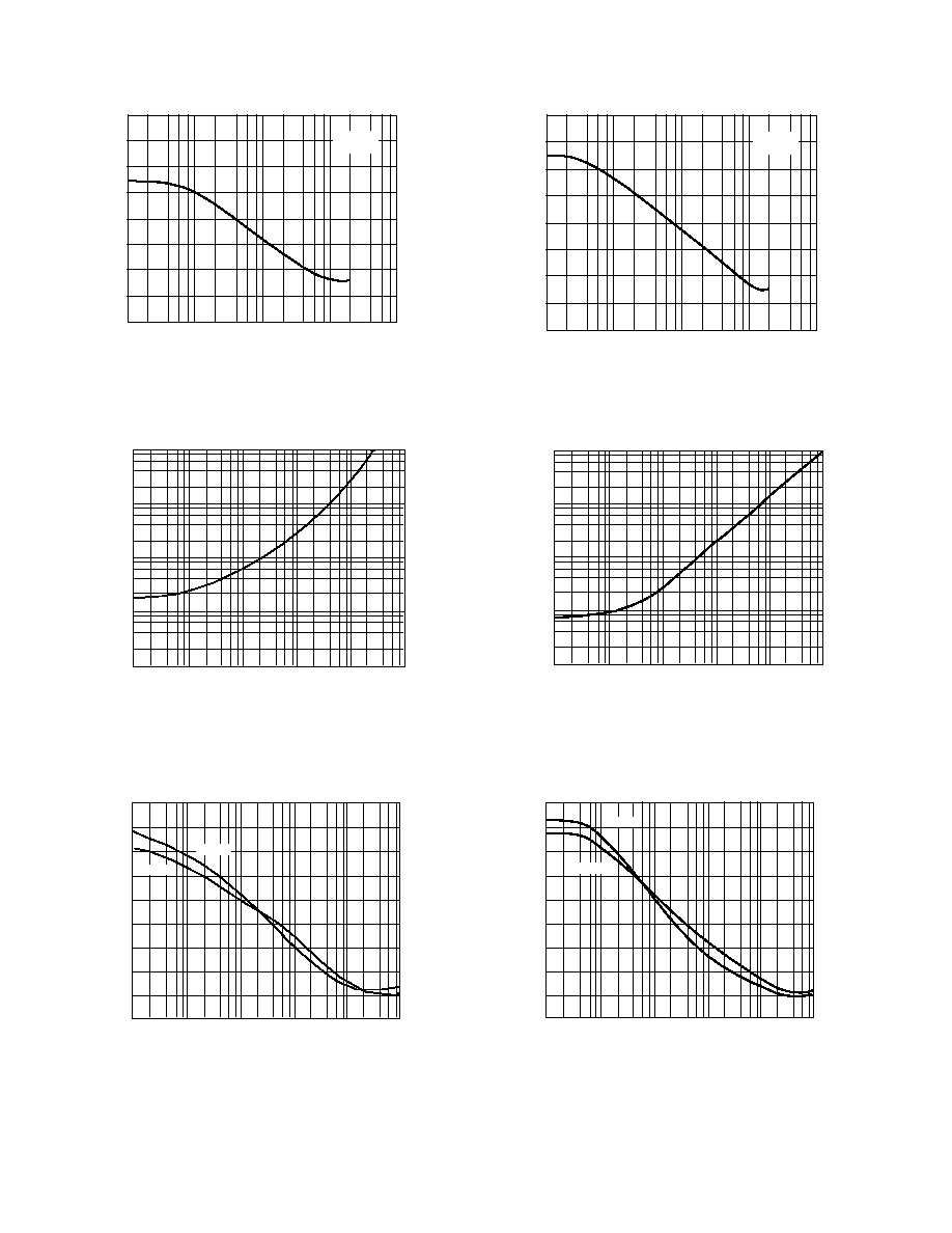
Figure 45. AD8047/AD8048 Output Swing vs. Temperature
JUNCTION TEMPERATURE
°
C
OPEN-LOOP GAIN V/V
2400
1600
1000
60
140
40
20
0
20
40
60
80
100
120
2200
1400
1200
2000
1800
2600
AD8048
AD8047
Figure 46. AD8047/AD8048 Open-Loop Gain vs.
Temperature
JUNCTION TEMPERATURE
°
C
94
60
92
90
88
86
84
82
80
78
76
40
20
0
20
40
60
80
100
120
140
+PSRR
AD8048
PSRR
PSRR
AD8047
+PSRR
AD8047
PSRR dB
AD8048
Figure 47. AD8047/AD8048 PSRR vs. Temperature
83.0
140
40
60
120
80
60
40
100
20
0
20
JUNCTION TEMPERATURE
°
C
CMRR dB
82.0
81.0
80.0
79.0
78.0
77.0
76.0
AD8047
AD8048
Figure 48. AD8047/AD8048 CMRR vs. Temperature
JUNCTION TEMPERATURE
°
C
7.5
5.5
60
140
40
20
0
20
40
60
80
100
120
7.0
6.0
5.0
4.5
6.5
8.0
SUPPLY CURRENT mA
±
6V
±
6V
±
5V
±
5V
AD8048
AD8047
AD8048
AD8047
Figure 49. AD8047/AD8048 Supply Current vs.
Temperature
JUNCTION TEMPERATURE
°
C
800
400
100
60
140
40
20
0
20
40
60
80
100
120
700
300
200
600
500
900
INPUT OFFSET VOLTAGE µV
AD8048
AD8047
Figure 50. AD8047/AD8048 Input Offset Voltage vs.
Temperature
REV. 0
12
AD8047/AD8048
THEORY OF OPERATION
General
The AD8047 and AD8048 are wide bandwidth, voltage feed-
back amplifiers. Since their open-loop frequency response fol-
lows the conventional 6 dB/octave roll-off, their gain bandwidth
product is basically constant. Increasing their closed-loop gain
results in a corresponding decrease in small signal bandwidth.
This can be observed by noting the bandwidth specification
between the AD8047 (gain of 1) and AD8048 (gain of 2).
Feedback Resistor Choice
The value of the feedback resistor is critical for optimum perfor-
mance on the AD8047 and AD8048. For maximum flatness at a
gain of 2, R
F
and R
G
should be set to 200
for the AD8048.
When the AD8047 is configured as a unity gain follower, R
F
should be set to 0
(no feedback resistor should be used) for
the plastic DIP and 66.5
for the SOIC.
V
IN
+V
S
6
7
2
4
3
V
OUT
G = 1 +
R
F
R
G
AD8047/48
R
TERM
0.1
µ
F
10
µ
F
V
S
0.1
µ
F
10
µ
F
R
G
R
F
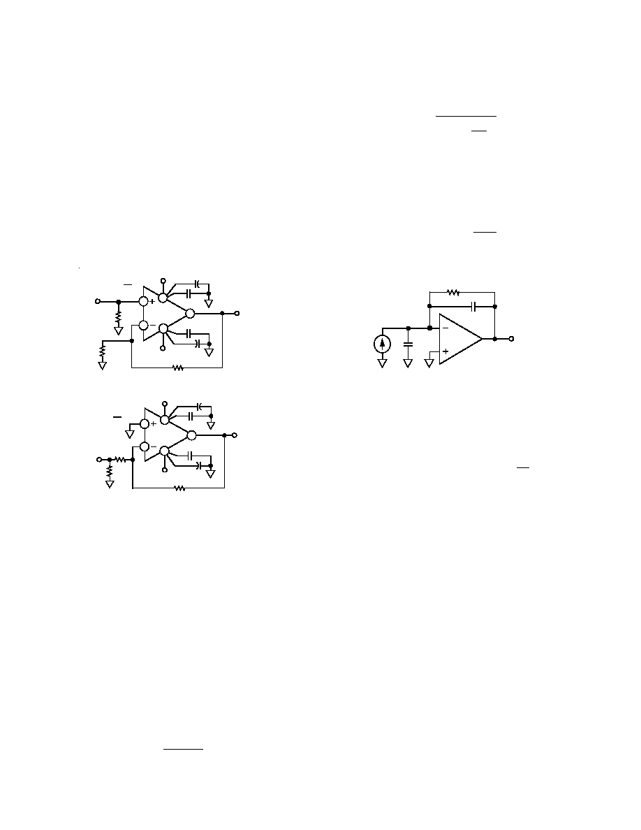
Figure 51. Noninverting Operation
V
IN
6
2
3
R
G
R
TERM
V
OUT
G =
R
F
R
G
AD8047/48
+V
S
7
0.1
µ
F
10
µ
F
4
V
S
0.1
µ
F
10
µ
F
R
F
Figure 52. Inverting Operation
When the AD8047 is used in the transimpedance (I to V) mode,
such as in photodiode detection, the value of R
F
and diode
capacitance (C
I
) are usually known. Generally, the value of R
F
selected will be in the k
range, and a shunt capacitor (C
F
)
across R
F
will be required to maintain good amplifier stability.
The value of C
F
required to maintain optimal flatness (<1 dB
Peaking) and settling time can be estimated as:
C
F
(2
O
C
I
R
F
1)/
O
2
R
F
2
[
]
1/2
where
O
is equal to the unity gain bandwidth product of the
amplifier in rad/sec, and C
I
is the equivalent total input
capacitance at the inverting input. Typically
O
= 800
×
10
6
rad/sec (see Open-Loop Frequency Response curve, Fig-
ure 17).
As an example, choosing R
F
= 10 k
and C
I
= 5 pF, requires
C
F
to be 1.1 pF (Note: C
I
includes both source and parasitic
circuit capacitance). The bandwidth of the amplifier can be
estimated using the C
F
calculated as:
f
3 dB
1.6
2
R
F
C
F
For general voltage gain applications, the amplifier bandwidth
can be closely estimated as:
f
3 dB
O
2
1
+
R
F
R
G
This estimation loses accuracy for gains of +2/1 or lower due
to the amplifier's damping factor. For these "low gain" cases,
the bandwidth will actually extend beyond the calculated value
(see Closed-Loop BW plots, Figures 15 and 26).
As a rule of thumb, capacitor C
F
will not be required if:
(R
F
R
G
)
×
C
I
NG
4
O
where NG is the Noise Gain (1 + R
F
/R
G
) of the circuit. For
most voltage gain applications, this should be the case.
R
F
V
OUT
AD8047
C
F
C
I
I
I
Figure 53. Transimpedance Configuration
Pulse Response
Unlike a traditional voltage feedback amplifier, where the slew
speed is dictated by its front end dc quiescent current and gain
bandwidth product, the AD8047 and AD8048 provide "on de-
mand" current that increases proportionally to the input "step"
signal amplitude. This results in slew rates (1000 V/
µ
s) compa-
rable to wideband current feedback designs. This, combined
with relatively low input noise current (1.0 pA/
Hz
), gives the
AD8047 and AD8048 the best attributes of both voltage and
current feedback amplifiers.
Large Signal Performance
The outstanding large signal operation of the AD8047 and
AD8048 is due to a unique, proprietary design architecture.
In order to maintain this level of performance, the maximum
180 V-MHz product must be observed, (e.g., @ 100 MHz,
V
O
1.8 V p-p) on the AD8047 and 250 V-MHz product on
the AD8048.
Power Supply Bypassing
Adequate power supply bypassing can be critical when optimiz-
ing the performance of a high frequency circuit. Inductance in
the power supply leads can form resonant circuits that produce
peaking in the amplifier's response. In addition, if large current
transients must be delivered to the load, then bypass capacitors
(typically greater than 1
µ
F) will be required to provide the best
settling time and lowest distortion. A parallel combination of at
least 4.7
µ
F, and between 0.1
µ
F and 0.01
µ
F, is recommended.
Some brands of electrolytic capacitors will require a small series
damping resistor
4.7
for optimum results.
Driving Capacitive Loads
The AD8047/AD8048 have excellent cap load drive capability
for high speed op amps as shown in Figures 55 and 57. How-
ever, when driving cap loads greater than 25 pF, the best fre-
quency response is obtained by the addition of a small series
resistance. It is worth noting that the frequency response of the
AD8047/AD8048
REV. 0
13
circuit when driving large capacitive loads will be dominated by
the passive roll-off of R
SERIES
and C
L
.
R
F
R
SERIES
R
L
1k
C
L
AD8047
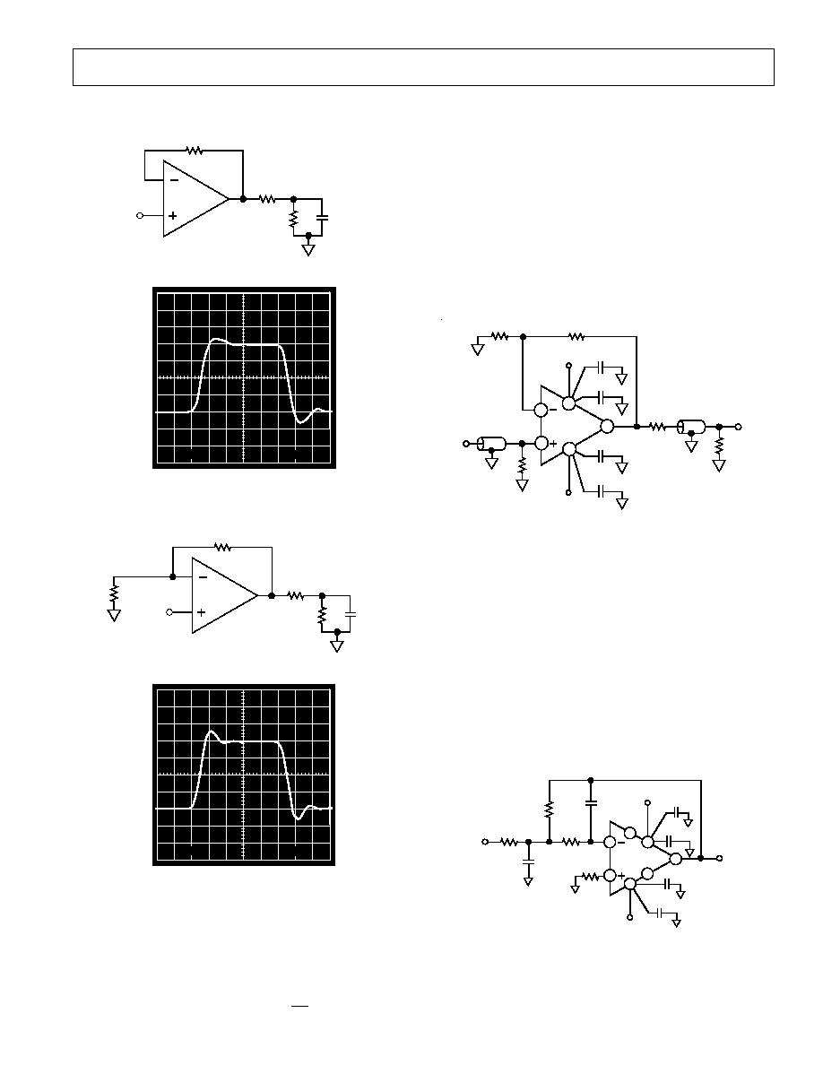
Figure 54. Driving Capacitive Loads
5ns
500mV
Figure 55. AD8047 Large Signal Transient Response;
V
O
= 2 V p-p, G = +1, R
F
= 0
, R
SERIES
= 0
, C
L
= 27 pF
R
F
R
SERIES
R
L
1k
C
L
AD8048
R
IN
Figure 56. Driving Capacitive Loads
5ns
500mV
Figure 57. AD8048 Large Signal Transient Response;
V
O
= 2 V p-p, G = +2, R
F
= R
IN
= 200
, R
SERIES
= 0
,
C
L
= 27 pF
APPLICATIONS
The AD8047 and AD8048 are voltage feedback amplifiers well
suited for such applications as photodetectors, active filters, and
log amplifiers. The devices' wide bandwidth (260 MHz), phase
margin (65
°
), low noise current (1.0 pA/
Hz
), and slew rate
(1000 V/
µ
s) give higher performance capabilities to these appli-
cations over previous voltage feedback designs.
With a settling time of 30 ns to 0.01% and 13 ns to 0.1%, the
devices are an excellent choice for DAC I/V conversion. The
same characteristics along with low harmonic distortion make
them a good choice for ADC buffering/amplification. With su-
perb linearity at relatively high signal frequencies, the AD8047
and AD8048 are ideal drivers for ADCs up to 12 bits.
Operation as a Video Line Driver
The AD8047 and AD8048 have been designed to offer out-
standing performance as video line drivers. The important
specifications of differential gain (0.01%) and differential phase
(0.02
°
) meet the most exacting HDTV demands for driving
video loads.
75
CABLE
200
200
75
CABLE
75
75
V
OUT
+V
S
V
S
75
V
IN
0.1
µ
F
10
µ
F
AD8047/
AD8048
3
2
7
0.1
µ
F
10
µ
F
4
6
Figure 58. Video Line Driver
Active Filters
The wide bandwidth and low distortion of the AD8047 and
AD8048 are ideal for the realization of higher bandwidth active
filters. These characteristics, while being more common in many
current feedback op amps, are offered in the AD8047 and AD8048
in a voltage feedback configuration. Many active filter configu-
rations are not realizable with current feedback amplifiers.
A multiple feedback active filter requires a voltage feedback
amplifier and is more demanding of op amp performance than
other active filter configurations such as the Sallen-Key. In
general, the amplifier should have a bandwidth that is at least
ten times the bandwidth of the filter if problems due to phase
shift of the amplifier are to be avoided.
Figure 59 is an example of a 20 MHz low pass multiple feed-
back active filter using an AD8048.
1
V
IN
R4
154
C1
50pF
C2
100pF
R1
154
AD8048
R3
78.7
+5V
0.1
µ
F
3
2
100
6
V
OUT
10
µ
F
5
0.1
µ
F
5V
10
µ
F
4
7
Figure 59. Active Filter Circuit
Choose:
F
O
= Cutoff Frequency = 20 MHz
= Damping Ratio = 1/Q = 2
REV. 0
14
AD8047/AD8048
H = Absolute Value of Circuit Gain =
R4
R1 = 1
Then:
k
=
2
F
O
C1
C2
=
4 C1(H
+
1)
2
R1
=
2 HK
R3
=
2 K (H
+
1)
R4
=
H(R1)
A/D Converter Driver
As A/D converters move toward higher speeds with higher reso-
lutions, there becomes a need for high performance drivers that
will not degrade the analog signal to the converter. It is desir-
able from a system's standpoint that the A/D be the element in
the signal chain that ultimately limits overall distortion. This
places new demands on the amplifiers used to drive fast, high
resolution A/Ds.
With high bandwidth, low distortion and fast settling time the
AD8047 and AD8048 make high performance A/D drivers for
advanced converters. Figure 60 is an example of an AD8047
used as an input driver for an AD872, a 12-bit, 10 MSPS A/D
converter.
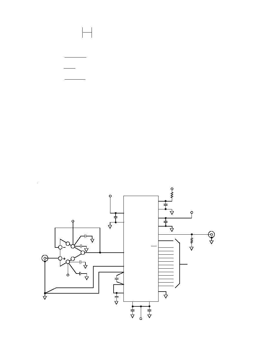
Layout Considerations
The specified high speed performance of the AD8047 and
AD8048 requires careful attention to board layout and compo-
nent selection. Proper RF design techniques and low pass para-
sitic component selection are mandatory
Figure 60. AD8047 Used as Driver for an AD872, a 12-Bit, 10 MSPS A/D Converter
MSB
BIT2
BIT3
BIT4
BIT5
BIT6
BIT7
BIT8
BIT9
BIT10
BIT11
BIT12
AV
DD
AGND
V
INA
REF GND
REF IN
REF OUT
AV
SS
AV
SS
AGND
OTR
CLK
DRGND
DRV
DD
DGND
DV
DD
19
18
17
16
15
14
13
12
11
10
9
8
24
25
3
26
28
27
1
20
21
23
22
6
7
4
5
V
INB
0.1
µ
F
5V ANALOG
AD872
1
6
3
2
5
1
µ
F
+5V ANALOG
AD8047
ANALOG IN
0.1
µ
F
0.1
µ
F
0.1
µ
F
DIGITAL OUTPUT
0.1
µ
F
0.1
µ
F
10
49.9
CLOCK INPUT
0.1
µ
F
0.1
µ
F
+5V ANALOG
+5V DIGITAL
+5V DIGITAL
5V
ANALOG
2
10
µ
F
10
µ
F
4
7
The PCB should have a ground plane covering all unused por-
tions of the component side of the board to provide a low im-
pedance path. The ground plane should be removed from the
area near the input pins to reduce stray capacitance.
Chip capacitors should be used for the supply bypassing (see
Figure 60). One end should be connected to the ground plane
and the other within 1/8 inch of each power pin. An additional
large (0.47
µ
F10
µ
F) tantalum electrolytic capacitor should be
connected in parallel, though not necessarily so close, to supply
current for fast, large signal changes at the output.
The feedback resistor should be located close to the inverting
input pin in order to keep the stray capacitance at this node to a
minimum. Capacitance variations of less than 1 pF at the in-
verting input will significantly affect high speed performance.
Stripline design techniques should be used for long signal traces
(greater than about 1 inch). These should be designed with a
characteristic impedance of 50
or 75
and be properly termi-
nated at each end.
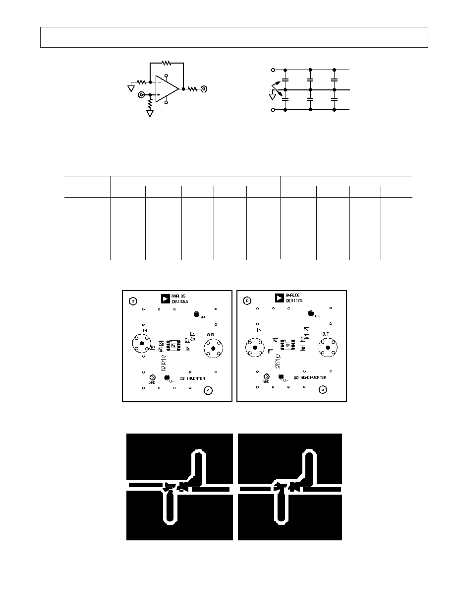
Evaluation Board
An evaluation board for both the AD8047 and AD8048 is avail-
able that has been carefully laid out and tested to demonstrate
that the specified high speed performance of the device can be
realized. For ordering information, please refer to the Ordering
Guide.
The layout of the evaluation board can be used as shown or
serve as a guide for a board layout.
AD8047/AD8048
REV. 0
15
Table I.
AD8047
AD8048
Component
1
+1
+2
+10
+101
1
+2
+10
+101
R
F
200
66.5
1 k
1 k
1 k
200
200
1 k
1 k
R
G
200
1 k
110
10
200
200
110
10
R
O
49.9
49.9
49.9
49.9
49.9
49.9
49.9
49.9
49.9
R
S
0
0
0
0
0
0
0
R
T
66.5
49.9
49.9
49.9
49.9
66.5
49.9
49.9
49.9
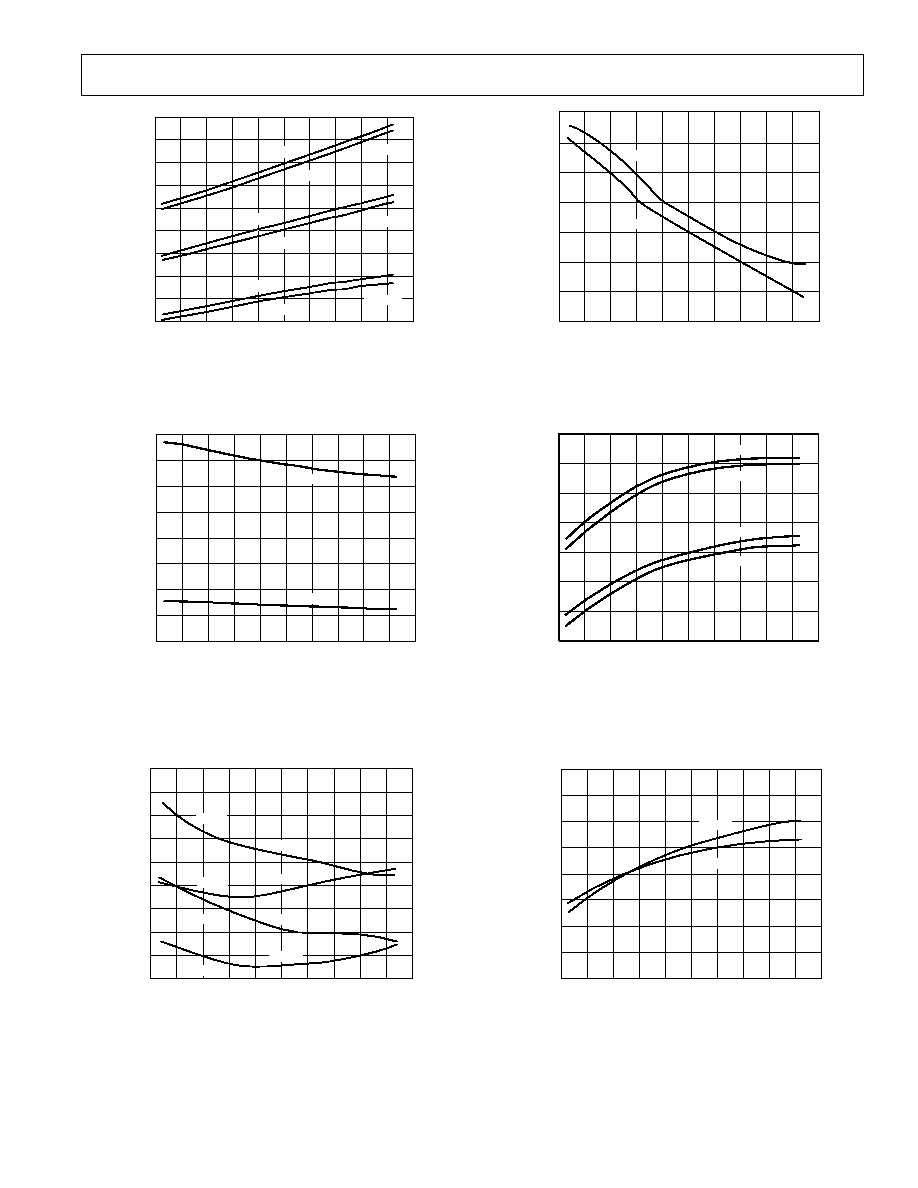
Small Signal
BW (3 dB)
90 MHz
260 MHz 95 MHz
10 MHz
1 MHz
250 MHz 250 MHz 22 MHz
2 MHz
Figure 61. Noninverting Configurations for Evaluation Boards
Figure 62. Evaluation Board Silkscreen (Top)
Figure 63. Board Layout (Solder Side)
SOIC (R)
INVERTER
SOIC (R)
NONINVERTER
SOIC (R)
INVERTER
SOIC (R)
NONINVERTER
C1
1000pF
C3
0.1
µ
F
C5
10
µ
F
C2
1000pF
C4
0.1
µ
F
C6
10
µ
F
+V
S
V
S
OPTIONAL
Noninverting Configuration
Supply Bypassing
R
F
R
O
+V
S
V
S
R
T
R
G
OUT
N
I
REV. 0
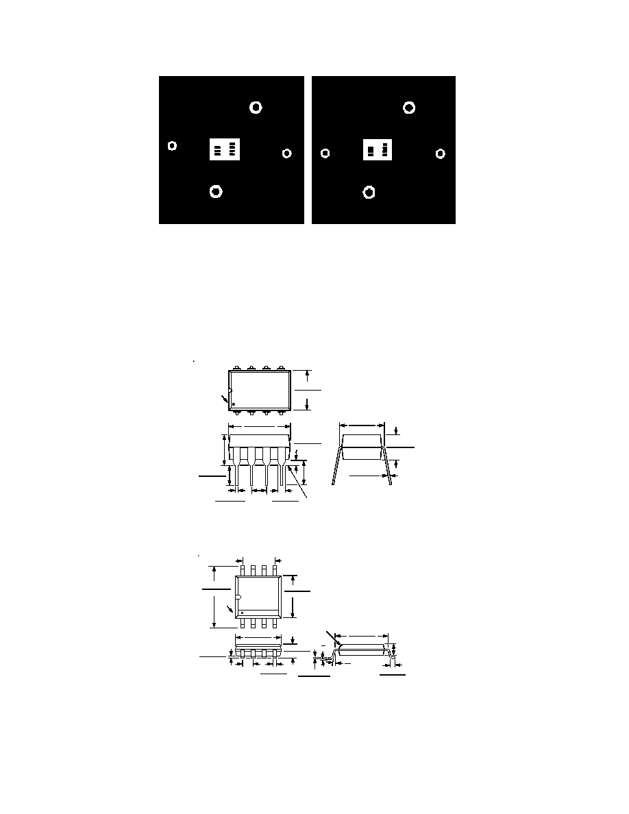
16
AD8047/AD8048
SOIC (R)
NONINVERTER
SOIC (R)
INVERTER
Figure 64. Board Layout (Component Side)
PRINTED IN U.S.A.
OUTLINE DIMENSIONS
Dimensions shown in inches and (mm).
8-Pin Plastic DIP
(N Package)
PIN 1
0.280 (7.11)
0.240 (6.10)
4
5
8
1
0.060 (1.52)
0.015 (0.38)
0.130
(3.30)
MIN
0.210
(5.33)
MAX
0.160 (4.06)
0.115 (2.93)
0.430 (10.92)
0.348 (8.84)
SEATING
PLANE
0.022 (0.558)
0.014 (0.356)
0.070 (1.77)
0.045 (1.15)
0.100
(2.54)
BSC
0.325 (8.25)
0.300 (7.62)
0.015 (0.381)
0.008 (0.204)
0.195 (4.95)
0.115 (2.93)
8-Pin Plastic SOIC
(R Package)
0.019 (0.48)
0.014 (0.36)
0.050
(1.27)
BSC
0.102 (2.59)
0.094 (2.39)
0.197 (5.01)
0.189 (4.80)
0.010 (0.25)
0.004 (0.10)
0.098 (0.2482)
0.075 (0.1905)
0.190 (4.82)
0.170 (4.32)
0.030 (0.76)
0.018 (0.46)
10
°
0
°
0.090
(2.29)
8
°
0
°
0.020 (0.051) x 45
°
CHAMF
1
8
5
4
PIN 1
0.157 (3.99)
0.150 (3.81)
0.244 (6.20)
0.228 (5.79)
0.150 (3.81)
C1995101/95