 | –≠–ª–µ–∫—Ç—Ä–æ–Ω–Ω—ã–π –∫–æ–º–ø–æ–Ω–µ–Ω—Ç: AD8051AR | –°–∫–∞—á–∞—Ç—å:  PDF PDF  ZIP ZIP |
REV. B
Information furnished by Analog Devices is believed to be accurate and
reliable. However, no responsibility is assumed by Analog Devices for its
use, nor for any infringements of patents or other rights of third parties
which may result from its use. No license is granted by implication or
otherwise under any patent or patent rights of Analog Devices.
a
AD8051/AD8052/AD8054
One Technology Way, P.O. Box 9106, Norwood, MA 02062-9106, U.S.A.
Tel: 781/329-4700
World Wide Web Site: http://www.analog.com
Fax: 781/326-8703
© Analog Devices, Inc., 1999
Low Cost, High Speed
Rail-to-Rail Amplifiers
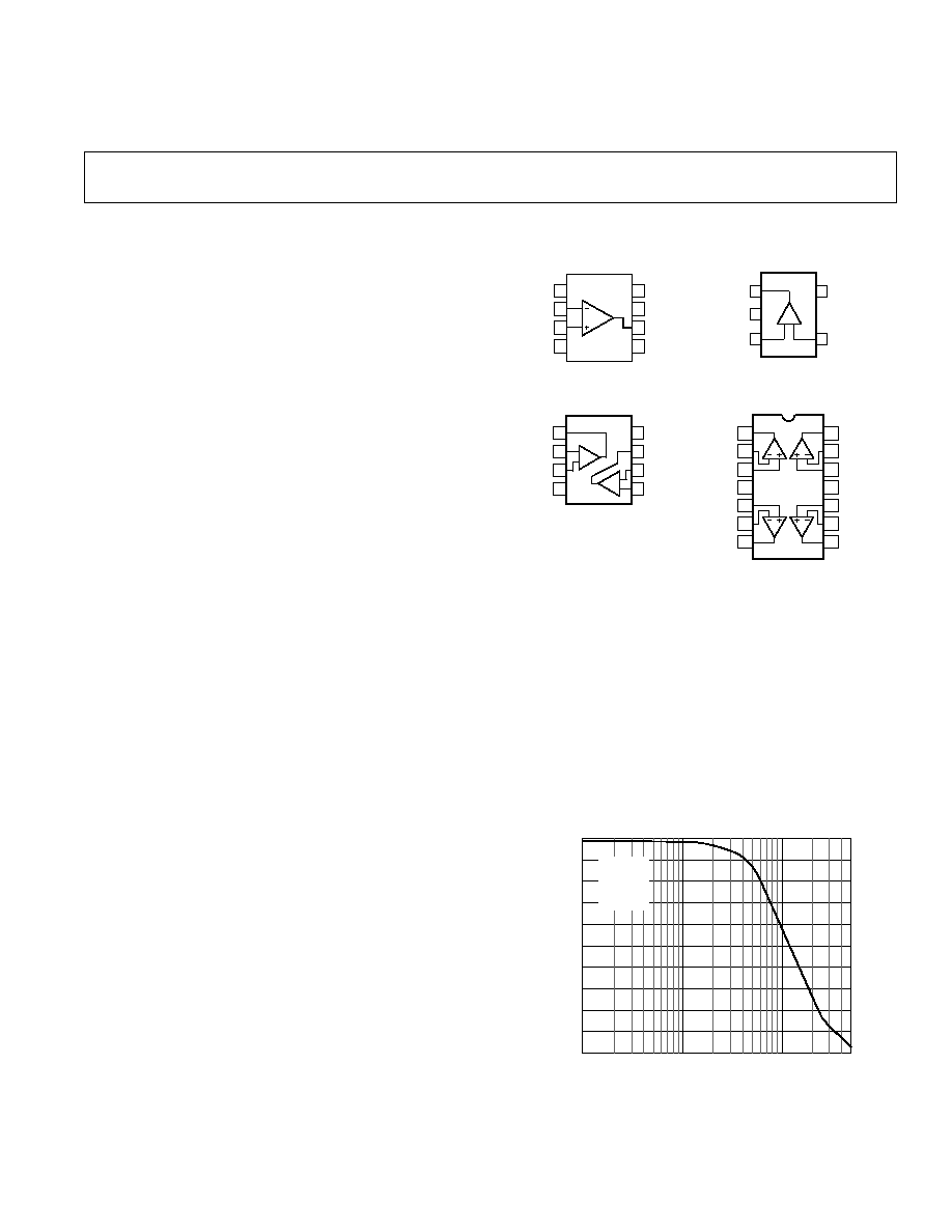
CONNECTION DIAGRAMS
(Top Views)
FEATURES
Low Cost Single (AD8051), Dual (AD8052) and Quad
(AD8054)
Voltage Feedback Architecture
Fully Specified at +3 V, +5 V and 5 V Supplies
Single Supply Operation
Output Swings to Within 25 mV of Either Rail
Input Voltage Range: ≠0.2 V to +4 V; V
S
= +5 V
High Speed and Fast Settling on +5 V:
110 MHz ≠3 dB Bandwidth (G = +1) (AD8051/AD8052)
150 MHz ≠3 dB Bandwidth (G = +1) (AD8054)
145 V/ s Slew Rate
50 ns Settling Time to 0.1%
Small Packaging
AD8051 Available in SOT-23-5
AD8052 Available in SOIC-8
AD8054 Available in TSSOP-14
Good Video Specifications (G = +2)
Gain Flatness of 0.1 dB to 20 MHz; R
L
= 150
0.03% Differential Gain Error; R
L
= 1K
0.03 Differential Phase Error; R
L
= 1K
Low Distortion
≠80 dBc Total Harmonic @ 1 MHz, R
L
= 100
Outstanding Load Drive Capability
Drives 45 mA, 0.5 V from Supply Rails (AD8051/AD8052)
Drives 50 pF Capacitive Load (G = +1) (AD8051/AD8052)
Low Power of 2.75 mA/Amplifier (AD8054)
Low Power of 4.4 mA/Amplifier (AD8051/AD8052)
APPLICATIONS
Coax Cable Driver
Active Filters
Video Switchers
A/D Driver
Professional Cameras
CCD Imaging Systems
CD/DVD ROM
PRODUCT DESCRIPTION
The AD8051 (single), AD8052 (dual) and AD8054 (quad) are
low cost, voltage feedback, high speed amplifiers designed to
operate on +3 V, +5 V or
±
5 V supplies. They have true single
supply capability with an input voltage range extending 200 mV
below the negative rail and within 1 V of the positive rail.
Despite their low cost, the AD8051/AD8052/AD8054 provide
excellent overall performance and versatility. The output volt-
age swing extends to within 25 mV of each rail, providing the
maximum output dynamic range with excellent overdrive recov-
ery. This makes the AD8051/AD8052/AD8054 useful for video
electronics such as cameras, video switchers or any high speed
portable equipment. Low distortion and fast settling make them
ideal for active filter applications.
The AD8051/AD8052/AD8054 offer low power supply cur-
rent and can operate on a single +3 V power supply. These
features are ideally suited for portable and battery powered
applications where size and power are critical.
The wide bandwidth and fast slew rate on a single +5 V supply
make these amplifiers useful in many general purpose, high speed
applications where dual power supplies of up to
±
6 V and single
supplies from +3 V to +12 V are needed.
All of this low cost performance is offered in an 8-lead SOIC,
along with a tiny SOT-23-5 package (AD8051), a
µ
SOIC
package (AD8052) and a TSSOP-14 (AD8054).
FREQUENCY ≠ MHz
4.5
0
50
0.1
1
10
3.0
1.5
1.0
0.5
4.0
3.5
2.0
2.5
5.0
PEAK-TO-PEAK OUTPUT VOLTAGE SWING
(THD
0.5%) ≠ Volts
V
S
= +5V
G = ≠1
R
F
= 2k
R
L
= 2k
Figure 1. Low Distortion Rail-to-Rail Output Swing
SOT-23-5 (RT)
R-8, SOIC (RM)
R-14, TSSOP-14 (RU-14)
SO-8
8
7
6
5
1
2
3
4
NC
≠IN
+IN
NC
+V
S
V
OUT
NC
≠V
S
AD8051
NC = NO CONNECT
8
7
6
5
1
2
3
4
+
≠
+
≠
OUT1
≠IN1
+IN1
OUT
+V
S
≠IN2
≠V
S
AD8052
+IN2
1
2
3
5
4 ≠IN
+IN
+V
S
V
OUT
AD8051
+ ≠
≠V
S
V+
+IN B
OUT B
OUT D
+IN D
V
+IN C
OUT C
AD8054
+IN A
OUT A
IN A
IN B
IN C
IN D
1
2
3
4
5
6
7
14
13
12
11
10
9
8

≠2≠
REV. B
AD8051/AD8052/AD8054≠SPECIFICATIONS
AD8051A/AD8052A
AD8054A
Parameter
Conditions
Min
Typ
Max Min
Typ
Max
Units
DYNAMIC PERFORMANCE
≠3 dB Small Signal Bandwidth
G = +1, V
O
= 0.2 V p-p
70
110
80
150
MHz
G = ≠1, +2, V
O
= 0.2 V p-p
50
60
MHz
Bandwidth for 0.1 dB Flatness
G = +2, V
O
= 0.2 V p-p,
R
L
= 150
to +2.5 V,
R
F
= 806
for AD8051A/AD8052A
20
MHz
R
F
= 200
for AD8054A
12
MHz
Slew Rate
G = ≠1, V
O
= 2 V Step
100
145
140
170
V/
µ
s
Full Power Response
G = +1, V
O
= 2 V p-p
35
45
MHz
Settling Time to 0.1%
G = ≠1, V
O
= 2 V Step
50
40
ns
NOISE/DISTORTION PERFORMANCE
Total Harmonic Distortion
1
f
C
= 5 MHz, V
O
= 2 V p-p, G = +2
≠67
≠68
dB
Input Voltage Noise
f = 10 kHz
16
16
nV/
Hz
Input Current Noise
f = 10 kHz
850
850
fA/
Hz
Differential Gain Error (NTSC)
G = +2, R
L
= 150
to +2.5 V
0.09
0.07
%
R
L
= 1 k
to +2.5 V
0.03
0.02
%
Differential Phase Error (NTSC)
G = +2, R
L
= 150
to +2.5 V
0.19
0.26
Degrees
R
L
= 1 k
to +2.5 V
0.03
0.05
Degrees
Crosstalk
f = 5 MHz, G = +2
≠60
≠60
dB
DC PERFORMANCE
Input Offset Voltage
1.7
10
1.7
12
mV
T
MIN
≠T
MAX
25
30
mV
Offset Drift
10
15
µ
V/
∞
C
Input Bias Current
1.4
2.5
2
4.5
µ
A
T
MIN
≠T
MAX
3.25
4.5
µ
A
Input Offset Current
0.1
0.75
0.2
1.2
µ
A
Open-Loop Gain
R
L
= 2 k
to +2.5 V
86
98
82
98
dB
T
MIN
≠T
MAX
96
96
dB
R
L
= 150
to +2.5 V
76
82
74
82
dB
T
MIN
≠T
MAX
78
78
dB
INPUT CHARACTERISTICS
Input Resistance
290
300
k
Input Capacitance
1.4
1.5
pF
Input Common-Mode Voltage Range
≠0.2 to 4
≠0.2 to 4
V
Common-Mode Rejection Ratio
V
CM
= 0 V to +3.5 V
72
88
70
86
dB
OUTPUT CHARACTERISTICS
Output Voltage Swing
R
L
= 10 k
to +2.5 V
0.015 to 4.985
0.03 to 4.975
V
R
L
= 2 k
to +2.5 V
0.1 to 4.9
0.025 to 4.975
0.125 to 4.875 0.05 to 4.95
V
R
L
= 150
to +2.5 V
0.3 to 4.625 0.2 to 4.8
0.55 to 4.4
0.25 to 4.65
V
Output Current
V
OUT
= 0.5 V to +4.5 V
45
30
mA
T
MIN
≠T
MAX
45
30
mA
Short Circuit Current
Sourcing
80
45
mA
Sinking
130
85
mA
Capacitive Load Drive
G = +1 (AD8051/AD8052)
50
pF
G = +2 (AD8054)
40
pF
POWER SUPPLY
Operating Range
3
12
3
12
V
Quiescent Current/Amplifier
4.4
5
2.75
3.275 mA
Power Supply Rejection Ratio
V
S
=
±
1 V
70
80
68
80
dB
OPERATING TEMPERATURE RANGE
≠40
+85
≠40
+85
∞
C
NOTES
1
Refer to Figure 15.
Specifications subject to change without notice.
(@ T
A
= +25 C, V
S
= +5 V, R
L
= 2 k to +2.5 V,
unless otherwise noted)

≠3≠
REV. B
AD8051/AD8052/AD8054
(@ T
A
= +25 C, V
S
= +3 V, R
L
= 2 k to +1.5 V, unless otherwise noted)
SPECIFICATIONS
AD8051A/AD8052A
AD8054A
Parameter
Conditions
Min
Typ
Max Min
Typ
Max
Units
DYNAMIC PERFORMANCE
≠3 dB Small Signal Bandwidth
G = +1, V
O
= 0.2 V p-p
70
110
80
135
MHz
G = ≠1, +2, V
O
= 0.2 V p-p
50
65
MHz
Bandwidth for 0.1 dB Flatness
G = +2, V
O
= 0.2 V p-p,
R
L
= 150
to 2.5 V,
R
F
= 402
for AD8051A/AD8052A
17
MHz
R
F
= 200
for AD8054A
10
MHz
Slew Rate
G = ≠1, V
O
= 2 V Step
90
135
110
150
V/
µ
s
Full Power Response
G = +1, V
O
= 1 V p-p
65
85
MHz
Settling Time to 0.1%
G = ≠1, V
O
= 2 V Step
55
55
ns
NOISE/DISTORTION PERFORMANCE
Total Harmonic Distortion
1
f
C
= 5 MHz, V
O
= 2 V p-p,
G = ≠1, R
L
= 100
to +1.5 V
≠47
≠48
dB
Input Voltage Noise
f = 10 kHz
16
16
nV/
Hz
Input Current Noise
f = 10 kHz
600
600
fA/
Hz
Differential Gain Error (NTSC)
G = +2, V
CM
= +1 V
R
L
= 150
to +1.5 V,
0.11
0.13
%
R
L
= 1 k
to +1.5 V
0.09
0.09
%
Differential Phase Error (NTSC)
G = +2, V
CM
= +1 V
R
L
= 150
to +1.5 V
0.24
0.3
Degrees
R
L
= 1 k
to +1.5 V
0.10
0.1
Degrees
Crosstalk
f = 5 MHz, G = +2
≠60
≠60
dB
DC PERFORMANCE
Input Offset Voltage
1.6
10
1.6
12
mV
T
MIN
≠T
MAX
25
30
mV
Offset Drift
10
15
µ
V/
∞
C
Input Bias Current
1.3
2.6
2
4.5
µ
A
T
MIN
≠T
MAX
3.25
4.5
µ
A
Input Offset Current
0.15
0.8
0.2
1.2
µ
A
Open-Loop Gain
R
L
= 2 k
80
96
80
96
dB
T
MIN
≠T
MAX
94
94
dB
R
L
= 150
74
82
72
80
dB
T
MIN
≠T
MAX
76
76
dB
INPUT CHARACTERISTICS
Input Resistance
290
300
k
Input Capacitance
1.4
1.5
pF
Input Common-Mode Voltage Range
≠0.2 to 2
≠0.2 to 2
V
Common-Mode Rejection Ratio
V
CM
= 0 V to 1.5 V
72
88
70
86
dB
OUTPUT CHARACTERISTICS
Output Voltage Swing
R
L
= 10 k
to +1.5 V
0.01 to 2.99
0.025 to 2.98
V
R
L
= 2 k
to +1.5 V
0.075 to 2.9 0.02 to 2.98
0.1 to 2.9
0.35 to 2.965
V
R
L
= 150
to +1.5 V
0.2 to 2.75
0.125 to 2.875
0.35 to 2.55
0.15 to 2.75
V
Output Current
V
OUT
= 0.5 V to +2.5 V
45
25
mA
T
MIN
≠T
MAX
45
25
mA
Short Circuit Current
Sourcing
60
30
mA
Sinking
90
50
mA
Capacitive Load Drive
G = +1 (AD8051/AD8052)
45
pF
G = +2 (AD8054)
35
pF
POWER SUPPLY
Operating Range
3
12
3
12
V
Quiescent Current/Amplifier
4.2
4.8
2.625
3.125 mA
Power Supply Rejection Ratio
V
S
= +0.5 V
68
80
68
80
dB
OPERATING TEMPERATURE RANGE
≠40
+85
≠40
+85
∞
C
NOTES
1
Refer to Figure 15.
Specifications subject to change without notice.

≠4≠
REV. B
AD8051/AD8052/AD8054≠SPECIFICATIONS
(@ T
A
= +25 C, V
S
= 5 V, R
L
= 2 k to Ground,
unless otherwise noted)
AD8051A/AD8052A
AD8054A
Parameter
Conditions
Min
Typ
Max Min
Typ
Max Units
DYNAMIC PERFORMANCE
≠3 dB Small Signal Bandwidth
G = +1, V
O
= 0.2 V p-p
70
110
85
160
MHz
G = ≠1, +2, V
O
= 0.2 V p-p
50
65
MHz
Bandwidth for 0.1 dB Flatness
G = +2, V
O
= 0.2 V p-p,
R
L
= 150
,
R
F
= 1.1 k
for AD8051A/AD8052A
20
MHz
R
F
= 200
for AD8054A
15
MHz
Slew Rate
G = ≠1, V
O
= 2 V Step
105
170
150
190
V/
µ
s
Full Power Response
G = +1, V
O
= 2 V p-p
40
50
MHz
Settling Time to 0.1%
G = ≠1, V
O
= 2 V Step
50
40
ns
NOISE/DISTORTION PERFORMANCE
Total Harmonic Distortion
f
C
= 5 MHz, V
O
= 2 V p-p, G = +2
≠71
≠72
dB
Input Voltage Noise
f = 10 kHz
16
16
nV/
Hz
Input Current Noise
f = 10 kHz
900
900
fA/
Hz
Differential Gain Error (NTSC)
G = +2, R
L
= 150
0.02
0.06
%
R
L
= 1 k
0.02
0.02
%
Differential Phase Error (NTSC)
G = +2, R
L
= 150
0.11
0.15
Degrees
R
L
= 1 k
0.02
0.03
Degrees
Crosstalk
f = 5 MHz, G = +2
≠60
≠60
dB
DC PERFORMANCE
Input Offset Voltage
1.8
11
1.8
13
mV
T
MIN
≠T
MAX
27
32
mV
Offset Drift
10
15
µ
V/
∞
C
Input Bias Current
1.4
2.6
2
4.5
µ
A
T
MIN
≠T
MAX
3.5
4.5
µ
A
Input Offset Current
0.1
0.75
0.2
1.2
µ
A
Open-Loop Gain
R
L
= 2 k
88
96
84
96
dB
T
MIN
≠T
MAX
96
96
dB
R
L
= 150
78
82
76
82
dB
T
MIN
≠T
MAX
80
80
dB
INPUT CHARACTERISTICS
Input Resistance
290
300
k
Input Capacitance
1.4
1.5
pF
Input Common-Mode Voltage Range
≠5.2 to 4
≠5.2 to 4
V
Common-Mode Rejection Ratio
V
CM
= ≠5 V to +3.5 V
72
88
70
86
dB
OUTPUT CHARACTERISTICS
Output Voltage Swing
R
L
= 10 k
≠4.98 to +4.98
≠4.97 to +4.97
V
R
L
= 2 k
≠4.85 to +4.85 ≠4.97 to +4.97
≠4.8 to +4.8 ≠4.9 to +4.9
V
R
L
= 150
≠4.45 to +4.3
≠4.6 to +4.6
≠4.0 to +3.8 ≠4.5 to +4.5
V
Output Current
V
OUT
= ≠ 4.5 V to +4.5 V
45
30
mA
T
MIN
≠T
MAX
45
30
mA
Short Circuit Current
Sourcing
100
60
mA
Sinking
160
100
mA
Capacitive Load Drive
G = +1 (AD8051/AD8052)
50
pF
G = +2 (AD8054)
40
pF
POWER SUPPLY
Operating Range
3
12
3
12
V
Quiescent Current/Amplifier
4.8
5.5
2.875
3.4
mA
Power Supply Rejection Ratio
V
S
=
±
1 V
68
80
68
80
dB
OPERATING TEMPERATURE RANGE
≠40
+85
≠40
+85
∞
C
Specifications subject to change without notice.

≠5≠
AD8051/AD8052/AD8054
REV. B
ABSOLUTE MAXIMUM RATINGS
1
Supply Voltage . . . . . . . . . . . . . . . . . . . . . . . . . . . . . . . . 12.6 V
Internal Power Dissipation
2
Small Outline Package (R) . . . Observe Power Derating Curves
SOT-23-5 Package . . . . . . . . Observe Power Derating Curves
µ
SOIC Package . . . . . . . . . . Observe Power Derating Curves
TSSOP-14 Package . . . . . . . Observe Power Derating Curves
Input Voltage (Common Mode) . . . . . . . . . . . . . . . . . . . .
±
V
S
Differential Input Voltage . . . . . . . . . . . . . . . . . . . . . . .
±
2.5 V
Output Short Circuit Duration
. . . . . . . . . . . . . . . . . . . . . . Observe Power Derating Curves
Storage Temperature Range (R) . . . . . . . . . ≠65
∞
C to +125
∞
C
Operating Temperature Range (A Grade) . . . ≠40
∞
C to +85
∞
C
Lead Temperature Range (Soldering 10 sec) . . . . . . . . +300
∞
C
NOTES
1
Stresses above those listed under Absolute Maximum Ratings may cause perma-
nent damage to the device. This is a stress rating only; functional operation of the
device at these or any other conditions above those indicated in the operational
section of this specification is not implied. Exposure to absolute maximum rating
conditions for extended periods may affect device reliability.
2
Specification is for device in free air:
8-Lead SOIC:
JA
= 155
∞
C/W
5-Lead SOT-23-5:
JA
= 240
∞
C/W
8-Lead
µ
SOIC:
JA
= 200
∞
C/W
14-Lead SOIC:
JA
= 120
∞
C/W
14-Lead TSSOP:
JA
= 180
∞
C/W
MAXIMUM POWER DISSIPATION
The maximum power that can be safely dissipated by the AD8051/
AD8052/AD8054 is limited by the associated rise in junction
temperature. The maximum safe junction temperature for
plastic encapsulated devices is determined by the glass transi-
tion temperature of the plastic, approximately +150
∞
C. Tempo-
rarily exceeding this limit may cause a shift in parametric
performance due to a change in the stresses exerted on the die by
the package. Exceeding a junction temperature of +175
∞
C for an
extended period can result in device failure.
While the AD8051/AD8052/AD8054 are internally short circuit
protected, this may not be sufficient to guarantee that the maxi-
mum junction temperature (+150
∞
C) is not exceeded under
all conditions. To ensure proper operation, it is necessary to ob-
serve the maximum power derating curves.
AMBIENT TEMPERATURE ≠ C
≠50
0
T
J
= +150 C
2.0
1.5
1.0
0.5
8-LEAD SOIC
PACKAGE
≠40 ≠30 ≠20 ≠10
0
10
20
30
40
50
60
70 80
90
SOIC
SOT-23-5
14-LEAD SOIC
MAXIMUM POWER DISSIPATION ≠ Watts
14-LEAD TSSOP-14
Figure 2. Plot of Maximum Power Dissipation vs.
Temperature for AD8051/AD8052/AD8054
CAUTION
ESD (electrostatic discharge) sensitive device. Electrostatic charges as high as 4000 V readily
accumulate on the human body and test equipment and can discharge without detection.
Although the AD8051/AD8052/AD8054 feature proprietary ESD protection circuitry, perma-
nent damage may occur on devices subjected to high energy electrostatic discharges. Therefore, proper
ESD precautions are recommended to avoid performance degradation or loss of functionality.
WARNING!
ESD SENSITIVE DEVICE
ORDERING GUIDE
Temperature
Package
Package
Brand
Model
Range
Descriptions
Options*
Code
AD8051AR
≠40
∞
C to +85
∞
C
8-Lead SOIC
SO-8
AD8051AR-REEL
≠40
∞
C to +85
∞
C
13" Tape and Reel
SO-8
AD8051AR-REEL7
≠40
∞
C to +85
∞
C
7" Tape and Reel
SO-8
AD8051ART-REEL
≠40
∞
C to +85
∞
C
13" Tape and Reel
RT-5
H2A
AD8051ART-REEL7
≠40
∞
C to +85
∞
C
7" Tape and Reel
RT-5
H2A
AD8052AR
≠40
∞
C to +85
∞
C
8-Lead SOIC
SO-8
AD8052AR-REEL
≠40
∞
C to +85
∞
C
13" Tape and Reel
SO-8
AD8052AR-REEL7
≠40
∞
C to +85
∞
C
7" Tape and Reel
SO-8
AD8052ARM
≠40
∞
C to +85
∞
C
8-Lead
µ
SOIC
RM-8
H4A
AD8052ARM-REEL
≠40
∞
C to +85
∞
C
13" Tape and Reel
RM-8
H4A
AD8052ARM-REEL7
≠40
∞
C to +85
∞
C
7" Tape and Reel
RM-8
H4A
AD8054AR
≠40
∞
C to +85
∞
C
14-Lead SOIC
R-14
AD8054AR-REEL
≠40
∞
C to +85
∞
C
13" Tape and Reel
R-14
AD8054AR-REEL7
≠40
∞
C to +85
∞
C
7" Tape and Reel
R-14
AD8054ARU
≠40
∞
C to +85
∞
C
14-Lead
µ
SOIC
RU-14
AD8054ARU-REEL
≠40
∞
C to +85
∞
C
13" Tape and Reel
RU-14
AD8054ARU-REEL7
≠40
∞
C to +85
∞
C
7" Tape and Reel
RU-14
*R = Small Outline; RM = Micro Small Outline; RT = Surface Mount; RU = TSSOP .

AD8051/AD8052/AD8054
≠6≠
REV. B
FREQUENCY ≠ MHz
3
2
≠7
0.1
1
10
100
V
S
= +5V
GAIN AS SHOWN
R
F
AS SHOWN
R
L
= 2k
V
O
= 0.2V p-p
G = +10
R
F
= 2k
G = +5
R
F
= 2k
G = +1
R
F
= 0
G = +2
R
F
= 2k
≠1
≠4
≠5
≠6
1
0
≠3
≠2
500
NORMALIZED GAIN ≠ dB
Figure 3. AD8051/AD8052 Normalized Gain vs.
Frequency; V
S
= +5 V
FREQUENCY ≠ MHz
3
2
≠7
0.1
500
1
10
100
≠1
≠4
≠5
≠6
1
0
≠3
≠2
V
S
= +3V
V
S
= 5V
V
S
= +5V
V
S
AS SHOWN
G = +1
R
L
= 2k
V
O
= 0.2V p-p
GAIN ≠ dB
Figure 4. AD8051/AD8052 Gain vs. Frequency
vs. Supply
FREQUENCY ≠ MHz
3
2
≠7
0.1
500
1
10
100
≠1
≠4
≠5
≠6
1
0
≠3
≠2
≠40 C
+25 C
+85 C
V
S
= +5V
G = +1
R
L
= 2k
V
O
= 0.2V p-p
TEMPERATURE AS SHOWN
GAIN ≠ dB
Figure 5. AD8051/AD8052 Gain vs. Frequency vs.
Temperature
1M
10M
100M
FREQUENCY ≠ Hz
3
0
≠3
≠6
≠7
100k
G = +1
R
F
= 0
V
S
= +5V
GAIN AS SHOWN
R
F
AS SHOWN
R
L
= 5k
V
O
= 0.2V p-p
G = +5
R
F
= 2k
G = +2
R
F
= 2k
G = +10
R
F
= 2k
≠5
≠4
≠2
≠1
5
4
2
1
500M
NORMALIZED GAIN ≠ dB
Figure 6. AD8054 Normalized Gain vs. Frequency;
V
S
= +5 V
G = +1
R
L
= 2k
C
L
= 5pF
V
O
= 0.2V p-p
+3V
+5V
5V
+3V
+5V
5V
6
2
≠3
100k
5
4
3
1
0
≠1
≠2
≠4
1M
10M
100M
FREQUENCY ≠ Hz
500M
GAIN ≠ dB
Figure 7. AD8054 Gain vs. Frequency vs. Supply
4
0
≠4
3
2
1
≠1
≠2
≠3
≠5
1
10
100
FREQUENCY ≠ MHz
V
S
= +5V
R
L
= 2k TO 2.5V
C
L
= 5pF
G = +1
V
O
= 0.2V p-p
≠40 C
+25 C
+85 C
GAIN ≠ dB
500
Figure 8. AD8054 Gain vs. Frequency vs. Temperature

≠7≠
AD8051/AD8052/AD8054
REV. B
FREQUENCY ≠ MHz
6.3
6.2
5.3
0.1
1
10
100
V
S
= +5V
G = +2
R
L
= 150
R
F
= 806
V
O
= 0.2V p-p
5.9
5.6
5.5
5.4
6.1
6.0
5.7
5.8
GAIN FLATNESS ≠ dB
Figure 9. AD8051/AD8052 0.1 dB Gain Flatness vs.
Frequency; G = +2
FREQUENCY ≠ MHz
9
8
≠1
0.1
500
1
10
100
5
2
1
0
7
6
3
4
V
S
AS SHOWN
G = +2
R
L
= 2k
R
F
= 2k
V
O
AS SHOWN
V
S
= +5V
V
O
= 2V p-p
V
S
= 5V
V
O
= 4V p-p
GAIN ≠ dB
Figure 10. AD8051/AD8052 Large Signal Frequency
Response; G = +2
FREQUENCY ≠ MHz
80
70
≠20
0.01
500
0.1
1
10
100
40
10
0
≠10
60
50
20
30
0
≠45
≠90
≠135
≠180
GAIN
PHASE
50
PHASE
MARGIN
V
S
= +5V
R
L
= 2k
OPEN-LOOP GAIN ≠ dB
PHASE ≠ Degrees
Figure 11. AD8051/AD8052 Open-Loop Gain and
Phase vs. Frequency
6.3
5.9
5.4
6.2
6.1
6.0
5.8
5.7
5.6
5.5
1
100
10
V
S
= +5V
R
F
= 200
R
L
= 150
G = +2
V
O
= 0.2V p-p
FREQUENCY ≠ MHz
GAIN FLATNESS ≠ dB
5.3
Figure 12. AD8054 0.1 dB Gain Flatness vs. Frequency;
G = +2
FREQUENCY ≠ MHz
0.1
500
1
10
100
V
S
= +5V
V
O
= 2V p-p
V
S
= 5V
V
O
= 4V p-p
V
S
AS SHOWN
G = +2
R
L
= 2k
R
F
= 2k
V
O
AS SHOWN
9
8
7
6
5
4
3
2
1
0
≠1
GAIN ≠ dB
Figure 13. AD8054 Large Signal Frequency Response;
G = +2
80
40
≠10
70
60
50
30
20
10
0
≠20
30k
100k
1M
10M
100M
GAIN
PHASE
45 PHASE
MARGIN
V
S
= +5V
R
L
= 2k
C
L
= 5pF
FREQUENCY ≠ Hz
180
135
90
45
0
500M
OPEN-LOOP GAIN ≠ dB
PHASE MARGIN ≠ Degrees
Figure 14. AD8054 Open-Loop Gain and Phase
Margin vs. Frequency

AD8051/AD8052/AD8054
≠8≠
REV. B
FUNDAMENTAL FREQUENCY ≠ MHz
1
2
3
4
5
6
7
8
9 10
20
30
110
70
80
90
100
50
60
40
V
O
= 2V p-p
V
S
= +3V, G = 1
R
F
= 2k , R
L
= 100
V
S
= +5V, G = +2
R
F
= 2k , R
L
= 100
V
S
= +5V, G = +1
R
L
= 100
V
S
= +5V, G = +2
R
F
= 2k , R
L
= 2k
V
S
= +5V, G = +1
R
L
= 2k
TOTAL HARMONIC DISTORTION ≠ dBc
Figure 15. Total Harmonic Distortion
OUTPUT VOLTAGE ≠ V p-p
0
5.0
0.5
1.0
1.5
2.0
2.5
3.0
3.5
4.0
4.5
30
40
120
80
90
100
110
60
70
50
130
140
V
S
= +5V
R
L
= 2k
G = +2
1MHz
5MHz
10MHz
WORST HARMONIC ≠ dBc
Figure 16. Worst Harmonic vs. Output Voltage
0.05
0.00
0.05
0.10
0.15
0.20
0.25
0.10
0
100
50
10
60
20
70
30
80
40
90
MODULATING RAMP LEVEL ≠ IRE
0.10
0.06
0
100
50
0.08
0.06
0.04
0.02
0.00
0.02
0.04
10
60
20
70
30
80
40
90
NTSC SUBSCRIBER (3.58MHz)
V
S
= +5, G = +2
R
F
= 2k , R
L
AS SHOWN
V
S
= +5, G = +2
R
F
= 2k , R
L
AS SHOWN
R
L
= 150
R
L
= 1k
R
L
= 1k
R
L
= 150
DIFFERENTIAL
GAIN ERROR ≠ %
DIFFERENTIAL
PHASE ERROR ≠ Degrees
Figure 17. AD8051/AD8052 Differential Gain and Phase
Errors
1000
100
1
10
10M
100
VOLTAGE NOISE ≠ nA
Hz
1k
10k
100k
1M
10
V
S
= +5V
FREQUENCY ≠ Hz
Figure 18. Input Voltage Noise vs. Frequency
100
10
0.1
10
10M
100
1k
10k
100k
1M
1
V
S
= +5V
FREQUENCY ≠ Hz
CURRENT NOISE ≠ pA
Hz
Figure 19. Input Current Noise vs. Frequency
0.10
≠0.10
0.05
0.00
≠0.05
1st
6th
2nd
7th
3rd
8th
4th
9th
5th
10th 11th
0.2
0.1
0.0
≠0.1
≠0.2
≠0.3
0.3
V
S
= +5, G = +2
R
F
= 2k , R
L
AS SHOWN
V
S
= +5, G = +2
R
F
= 2k ,
R
L
AS SHOWN
R
L
= 150
R
L
= 1k
R
L
= 1k
R
L
= 150
NTSC SUBSCRIBER (3.58MHz)
1st
6th
2nd
7th
3rd
8th
4th
9th
5th
10th 11th
DIFFERENTIAL
GAIN ≠ %
DIFFERENTIAL
PHASE ≠ Degrees
MODULATING RAMP LEVEL ≠ IRE
Figure 20. AD8054 Differential Gain and Phase Errors

≠9≠
AD8051/AD8052/AD8054
REV. B
FREQUENCY ≠ MHz
≠10
≠20
0.1
500
1
10
100
≠50
≠80
≠90
≠100
≠30
≠40
≠70
≠60
V
S
= +5V
R
F
= 2k
R
L
= 2k
V
O
= 2V p-p
CROSSTALK ≠ dB
Figure 21. AD8052 Crosstalk (Output-to-Output) vs.
Frequency
FREQUENCY ≠ MHz
0
≠10
≠100
0.03
500
0.1
1
10
100
≠40
≠70
≠80
≠90
≠20
≠30
≠60
≠50
V
S
= +5V
CMRR ≠ dB
Figure 22. CMRR vs. Frequency
FREQUENCY ≠ MHz
100
0.1
1
10
100
500
3.1
0.1
0.031
0.01
31
10
0.31
1
V
S
= 5V
G = 1
OUTPUT RESISTANCE ≠
Figure 23. Closed Loop Output Resistance vs. Frequency
≠10
≠50
≠100
≠20
≠30
≠40
≠60
≠70
≠80
≠90
≠110
0.1
1
10
100
FREQUENCY ≠ MHz
500
V
S
= 5V
R
F
= 1k
R
L
= AS SHOWN
V
O
= 2V p-p
R
L
= 1k
R
L
= 100
CROSSTALK ≠ dB
Figure 24. AD8054 Crosstalk (Output-to-Output) vs.
Frequency
FREQUENCY ≠ MHz
20
≠10
≠30
≠50
≠70
10
0
≠20
≠40
≠60
≠80
1
500
10
100
0.1
0.01
V
S
= +5V
≠PSRR
+PSRR
PSRR ≠ dB
Figure 25. PSRR vs. Frequency
INPUT STEPS ≠ Volts p-p
60
0
40
30
20
10
50
70
0.5
2
1
1.5
SETTING TIME TO 0.1%
ns
AD8051/AD8052
AD8054
V
S
= 5V
G = 1
R
L
= 2k
Figure 26. Settling Time vs. Input Step
AD8051/AD8052/AD8054
≠10≠
REV. B
LOAD CURRENT ≠ mA
1.00
0.30
0
0
65
5 10 15 20 25 30 35 40 45 50 55 60
0.90
0.40
0.20
0.10
0.70
0.50
0.80
0.60
70 75 80 85
V
OH
= +85 C
V
OH
= +25 C
V
OH
= ≠40 C
V
OL
= +85 C
V
OL
= +25 C
V
OL
= ≠40 C
V
S
= +5V
OUTPUT SATURATION VOLTAGE ≠ Volts
Figure 27. AD8051/AD8052 Output Saturation Voltage vs.
Load Current
100
90
60
0
5
0.5
1
1.5
2
2.5
3
3.5
4
4.5
80
70
R
L
= 2k
R
L
= 150
V
S
= +5V
OPEN-LOOP GAIN ≠ dB
OUTPUT VOLTAGE ≠ Volts
Figure 28. Open-Loop Gain vs. Output Voltage
LOAD CURRENT ≠ mA
1.00
0.500
0.00
0.875
0.750
0.250
0.125
0.625
0.375
0
30
3
6
9
12
15
18
21
24
27
V
S
= +5V
+5V ≠V
OH
(+25 C)
+5V ≠V
OH
(≠55 C)
+5V ≠V
OH
(+125 C)
V
OL
(+125 C)
V
OL
(+25 C)
V
OL
(≠55 C)
OUTPUT SATURATION VOLTAGE ≠ Volts
Figure 29. AD8054 Output Saturation Voltage vs. Load
Current

≠11≠
AD8051/AD8052/AD8054
REV. B
1.50V
Figure 30. 100 mV Step Response, G = +1
20ns
2.50
2.60
2.40
Figure 31. AD8051/AD8052 200 mV Step Response;
V
S
= +5 V, G = +1
3.5
2.5
1.5
VOLTS
Figure 32. Large Signal Step Response; V
S
= +5 V, G = +2
5
2.5
VOLTS
Figure 33. Output Swing; G = ≠1, R
L
= +2 k
2.55
2.50
2.45
VOLTS
Figure 34. AD8054 100 mV Step Response; V
S
= +5 V,
G = +1
4
3
2
1
1
2
3
4
Figure 35. Large Signal Step Response; V
S
=
±
5 V, G = +1
AD8051/AD8052/AD8054
≠12≠
REV. B
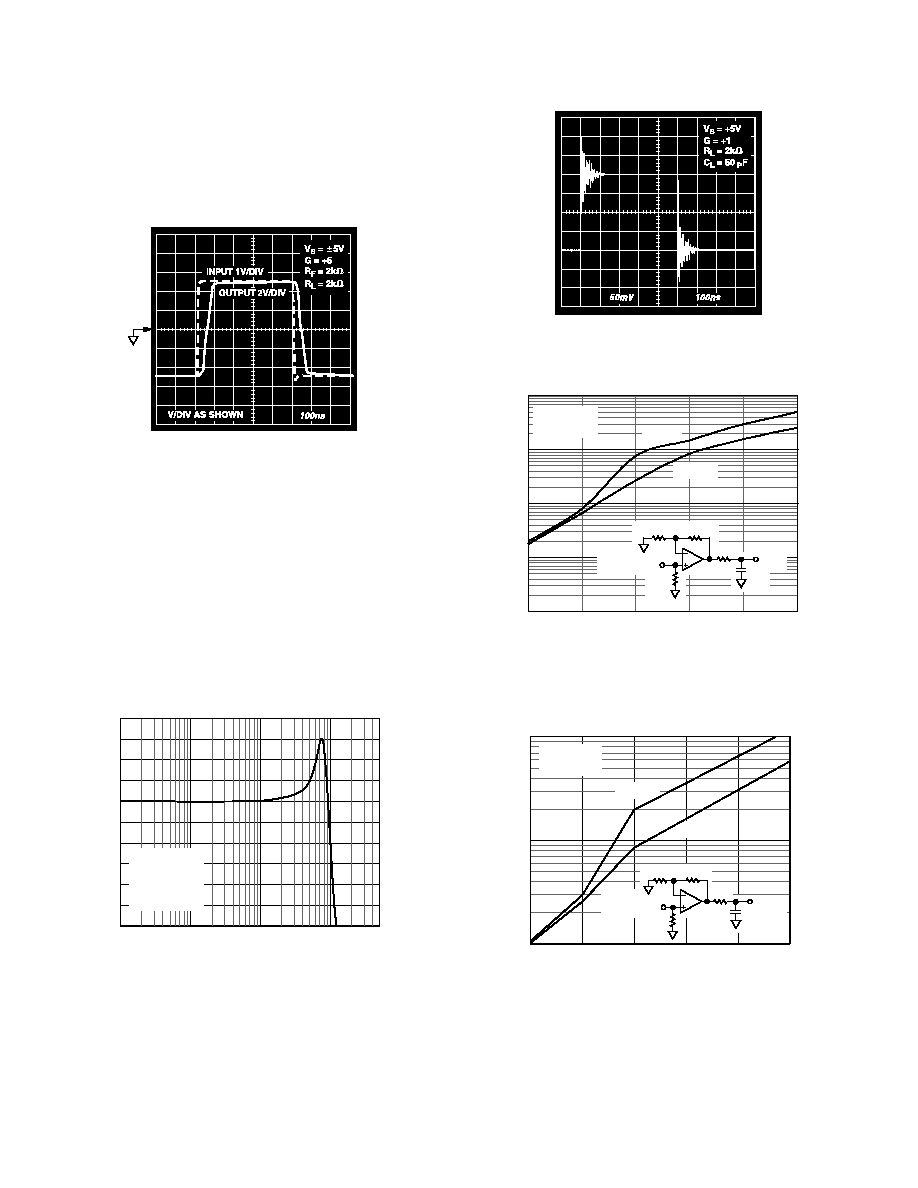
Overdrive Recovery
Overdrive of an amplifier occurs when the output and/or input
range are exceeded. The amplifier must recover from this over-
drive condition. As shown in Figure 36, the AD8051/AD8052/
AD8054 recovers within 60 ns from negative overdrive and
within 45 ns from positive overdrive.
Figure 36. Overdrive Recovery
Driving Capacitive Loads
Consider the AD8051/AD8052 in a closed-loop gain of +1 with
+V
S
= 5 V and a load of 2 k
in parallel with 50 pF. Figures 37
and 38 show its frequency and time domain responses, respec-
tively, to a small-signal excitation. The capacitive load drive of
the AD8051/AD8052/AD8054 can be increased by adding a
low valued resistor in series with the load. Figures 39 and 40
show the effect of a series resistor on capacitive drive for varying
voltage gains. As the closed-loop gain is increased, the larger
phase margin allows for larger capacitive loads with less peak-
ing. Adding a series resistor with lower closed-loop gains ac-
complishes the same effect. For large capacitive loads, the
frequency response of the amplifier will be dominated by the
roll-off of the series resistor and the load capacitance.
FREQUENCY ≠ MHz
500
0.1
1
10
100
V
S
= +5V
G = +1
R
L
= 2k
C
L
= 50pF
V
O
= 200mV p-p
8
6
4
2
0
2
4
6
8
10
GAIN ≠ dB
Figure 37. AD8051/AD8052 Closed-Loop Frequency
Response: C
L
= 50 pF
2.60
2.55
2.50
2.45
2.40
Figure 38. AD8051/AD8052 200 mV Step Response:
C
L
= 50 pF
V
S
= +5V
30%
OVERSHOOT
R
S
= 3
R
S
= 0
R
G
R
F
C
L
R
S
V
OUT
V
IN
100mV STEP
50
10000
1000
1
1
6
2
CAPACITIVE LOAD
P
F
3
4
5
100
10
A
C L
≠ V/V
Figure 39. AD8051/AD8052 Capacitive Load Drive vs.
Closed-Loop Gain
V
S
= +5V
30%
OVERSHOOT
R
G
R
F
C
L
R
S
V
OUT
V
IN
100mV STEP
50
R
S
= 10
R
S
= 0
A
C L
≠ V/V
1000
100
10
1
6
2
3
4
5
CAPACITIVE LOAD ≠ pF
Figure 40. AD8054 Capacitive Load Drive vs. Closed-Loop
Gain
Circuit Description
The AD8051/AD8052/AD8054 is fabricated on Analog Devices'
proprietary eXtra-Fast Complementary Bipolar (XFCB) pro-
cess, which enables the construction of PNP and NPN transis-
tors with similar f
T
s in the 2 GHz≠4 GHz region. The process is
dielectrically isolated to eliminate the parasitic and latch-up
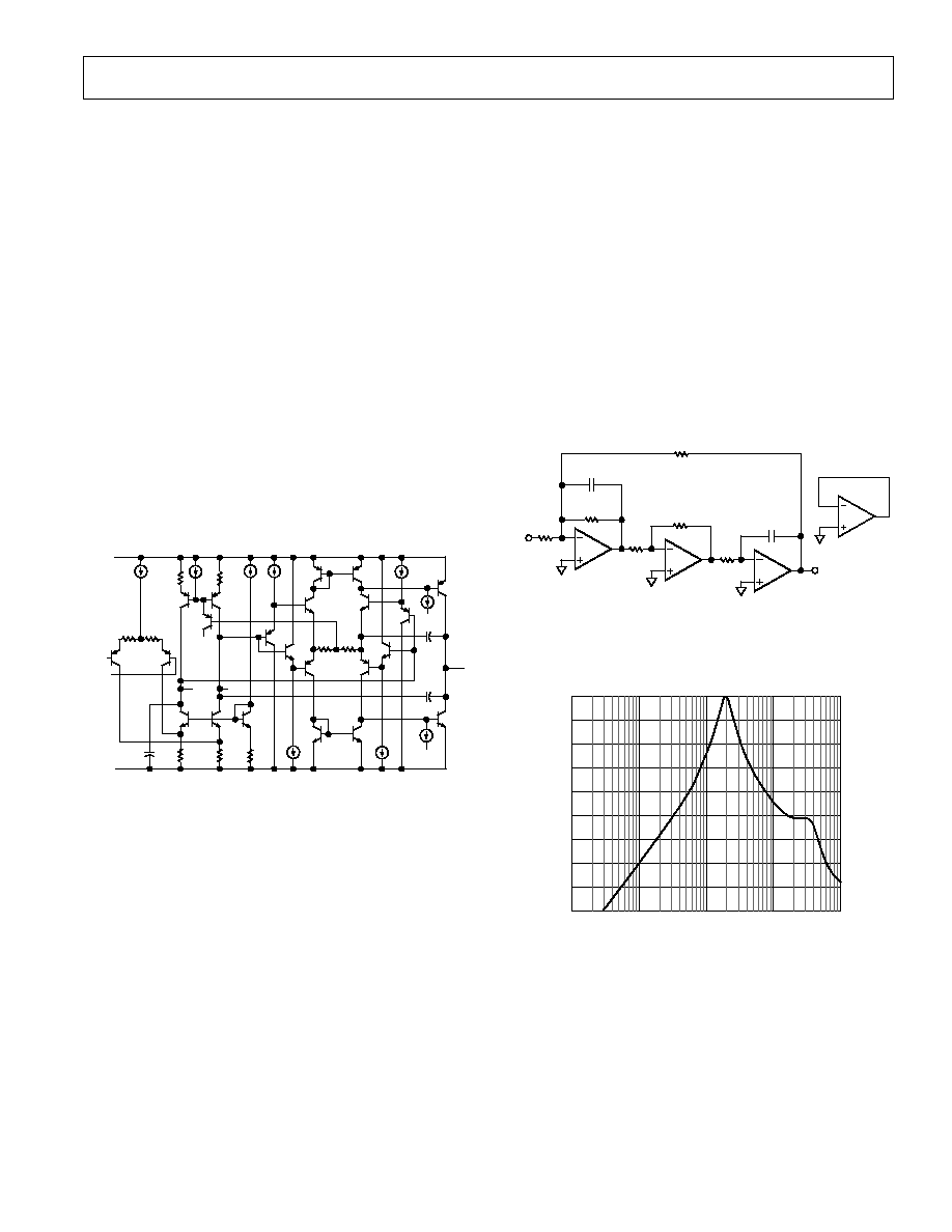
≠13≠
AD8051/AD8052/AD8054
REV. B
problems caused by junction isolation. These features allow the
construction of high frequency, low distortion amplifiers with low
supply currents. This design uses a differential output input stage
to maximize bandwidth and headroom (see Figure 1). The smaller
signal swings required on the first stage outputs (nodes S1P, S1N)
reduce the effect of nonlinear currents due to junction capacitances
and improve the distortion performance. With this design har-
monic distortion of ≠80 dBc @ 1 MHz into 100
with V
OUT
=
2 V p-p (Gain = +1) on a single 5 V supply is achieved.
The inputs of the device can handle voltages from ≠0.2 V below
the negative rail to within 1 V of the positive rail. Exceeding
these values will not cause phase reversal; however, the input
ESD devices will begin to conduct if the input voltages exceed
the rails by greater than 0.5 V. During this overdrive condition,
the output stays at the rail.
The rail-to-rail output range of the AD8051/AD8052/AD8054
is provided by a complementary common-emitter output stage.
High output drive capability is provided by injecting all out-
put stage predriver currents directly into the bases of the output
devices Q8 and Q36. Biasing of Q8 and Q36 is accomplished by
I8 and I5, along with a common-mode feedback loop (not
shown). This circuit topology allows the AD8051/AD8052 to drive
45 mA of output current and the AD8054 to drive 30 mA of out-
put current with the outputs within 0.5 V of the supply rails.
I10
R39
V
EE
I2
I3
Q25
Q51
R23 R27
I9
Q36
I5
V
EE
C3
V
OUT
C9
I8
V
CC
I11
I7
R3
R21
R5
Q3
SIP
SIN
C7
V
EE
V
IN
N
V
IN
P
Q4
R15 R2
V
CC
R26
Q50
Q22
Q21
Q27
Q7
Q8
Q23
Q31
Q39
Q13
Q1
Q24
Q47
Q11
Q2
Q5
Q40
Figure 41. AD8051/AD8052 Simplified Schematic
APPLICATIONS
Layout Considerations
The specified high speed performance of the AD8051/AD8052/
AD8054 requires careful attention to board layout and compo-
nent selection. Proper RF design techniques and low-parasitic
component selection are necessary.
The PCB should have a ground plane covering all unused por-
tions of the component side of the board to provide a low im-
pedance path. The ground plane should be removed from the
area near the input pins to reduce the parasitic capacitance.
Chip capacitors should be used for the supply bypassing. One
end should be connected to the ground plane and the other
within 3 mm of each power pin. An additional large (4.7
µ
F to
10
µ
F) tantalum electrolytic capacitor should be connected in
parallel, but not necessarily so close, to supply current for fast,
large signal changes at the output.
The feedback resistor should be located close to the inverting
input pin in order to keep the parasitic capacitance at this node
to a minimum. Parasitic capacitance of less than 1 pF at the
inverting input can significantly affect high speed performance.
Stripline design techniques should be used for long signal traces
(greater than about 25 mm). These should be designed with a
characteristic impedance of 50
or 75
and be properly termi-
nated at each end.
Active Filters
Active filters at higher frequencies require wider bandwidth op
amps to work effectively. Excessive phase shift produced by
lower frequency op amps can significantly impact active filter
performance.
Figure 42 shows an example of a 2 MHz biquad bandwidth
filter that uses three op amps of an AD8054. Such circuits are
sometimes used in medical ultrasound systems to lower the
noise bandwidth of the analog signal before A/D conversion.
Please note that the unused amplifiers' inputs should be tied to
ground.
12
13
14
2
1
R1
3k
V
IN
R2
2k
C1
50pF
R3
2k
6
5
7
R6
1k
R5
2k
9
10
8
AD8054
AD8054
C2
50pF
V
OUT
R4
2k
3
AD8054
Figure 42. 2 MHz Biquad Bandpass Filter Using AD8054
The frequency response of the circuit is shown in Figure 43.
FREQUENCY ≠ Hz
10k
100M
100k
1M
10M
0
10
20
30
40
GAIN ≠ dB
Figure 43. Frequency Response of 2 MHz Bandpass
Biquad Filter
A/D and D/A Applications
Figure 44 is a schematic showing the AD8051 used as a driver
for an AD9201, a 10-bit 20 MSPS dual A/D converter. This
converter is designed to convert I and Q signals in communica-
tion systems. In this application, only the I channel is being
driven. The I channel is enabled by applying a logic HIGH to
SELECT, Pin 27.
The AD8051 is running from a dual supply and is configured
for a gain of +2. The input signal is terminated in 50
and
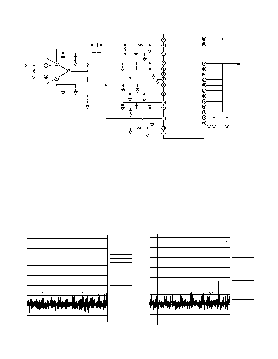
AD8051/AD8052/AD8054
≠14≠
REV. B
AD8051
+5V
0.1 F
10 F
10 F
0.1 F
V
REF
AVDD
SELECT
INA-I
V
DD
10pF
CLK
SLEEP
D9
D1
D2
D3
D4
D5
D6
D7
D0
DVDD
AVSS
REFSENSE
AD9201
DVSS
THREE≠STATE
INB-I
REFT-I
REFB-I
REFB-Q
REFT-Q
INB-Q
INA-Q
D8
5V
DATA OUT
0.1 F
22
10pF
22
10 F
0.1 F
5V
0.1 F
10 F
0.1 F
22
22
5V
22
1k
50
1k
10pF
10pF
0.1 F
10 F
0.1 F
0.1 F
10 F
0.1 F
1k
0.1 F
10 F
0.01 F
0.33 F
Figure 44. AD8051 Driving an AD9201, a 10-Bit 20 MSPS A/D Converter
applied to the noninverting input of the AD8051. The amplifier
output is 2 V p-p, which is the maximum input range of the
AD9201. The 22
series resistor limits the maximum current
that flows and helps to lower the distortion of the A/D.
The AD9201 has differential inputs for each channel. These are
designated the A and B inputs. The B inputs of each channel are
connected to VREF (Pin 8) which supplies a positive reference
of 2.5 V. Each of the B inputs has a small low pass filter that
also helps to reduce distortion.
The output of the op amp is ac coupled into INA-I (Pin 2) via
two parallel capacitors to provide good high frequency and low
frequency coupling. The 1 k
resistor references the signal to
VREF that is applied to INB-I. Thus, INA-I will swing both
positive and negative with respect to the bias voltage applied to
INB-I.
With the sampling clock running at 20 MSPS, the A/D output
was analyzed with a digital analyzer. Two input frequencies
were used, 1 MHz and 9.5 MHz, which is just short of the
Nyquist frequency. These signals were well filtered to minimize
any harmonics.
Figure 45 shows the FFT response of the A/D for the case of
1 MHz analog input. The SFDR is 71.66 dB and the A/D is
producing 8.8 ENOB (effective number of bits). When the
analog frequency was raised to 9.5 MHz, the SFDR was re-
duced to 60.18 dB and the A/D operated with 8.46 ENOBs as
shown in Figure 46. The inclusion of the AD8051 in the circuit
had no worsening of the distortion performance of the AD9201.
PART#
0
FCLK
FUND
VIN
THD
SNR
SINAD
ENOB
SFDR
2ND
3RD
4TH
5TH
6TH
7TH
8TH
9TH
FFTSIZE 8192
20.0E 6
998.5E 3
0.51dB
68.13
54.97
54.76
8.80
71.66
74.53
76.06
76.35
79.05
80.36
75.08
88.12
77.87
10.0
5.0
0.0
5.0
10.0
15.0
20.0
25.0
30.0
35.0
40.0
45.0
50.0
55.0
60.0
65.0
70.0
75.0
80.0
85.0
90.0
95.0
100.0
105.0
110.0
115.0
120.0
0.0E 0
1.0E 6
2.0E 6
3.0E 6
4.0E 6
5.0E 6
6.0E 6
7.0E 6
8.0E 6
9.0E 6
10.0E 6
2ND
3RD
4TH
5TH
6TH
7TH
8TH
9TH
FUND
Figure 45. FFT Plot for AD8051 Driving the AD9201 at
1 MHz
10.0
5.0
0.0
5.0
10.0
15.0
20.0
25.0
30.0
35.0
40.0
45.0
50.0
55.0
60.0
65.0
70.0
75.0
80.0
85.0
90.0
95.0
100.0
105.0
110.0
115.0
120.0
0.0E 0
1.0E 6
2.0E 6
3.0E 6
4.0E 6
5.0E 6
6.0E 6
7.0E 6
8.0E 6
9.0E 6
10.0E 6
PART#
0
FCLK
FUND
VIN
THD
SNR
SINAD
ENOB
SFDR
2ND
3RD
4TH
5TH
6TH
7TH
8TH
9TH
FFTSIZE 8192
20.0E 6
9.5E 6
0.44dB
57.08
54.65
52.69
8.46
60.18
60.18
60.23
82.01
78.83
81.28
77.28
84.54
92.78
FUND
3RD
4TH
6TH
7TH
8TH
2ND
Figure 46. FFT Plot for AD8051 Driving the AD9201 at
9.5 MHz

≠15≠
AD8051/AD8052/AD8054
REV. B
Sync Stripper
Synchronizing pulses are sometimes carried on video signals so
as not to require a separate channel to carry the synchronizing
information. However, for some functions, like A/D conversion,
it is not desirable to have the sync pulses on the video signal.
These pulses will reduce the dynamic range of the video signal
and do not provide any useful information for such a function.
A sync stripper will remove the synchronizing pulses from a
video signal while passing all the useful video information. Fig-
ure 47 shows a practical single supply circuit that uses only a
single AD8051. It is capable of directly driving a reverse termi-
nated video line.
AD8051
0.1 F
10 F
+
R1
1k
R2
1k
100
TO A/D
+0.8V
(OR 2 V
BLANK
)
V
IN
+3V OR +5V
V
BLANK
GROUND
+0.4V
VIDEO WITH SYNC
GROUND
VIDEO WITHOUT SYNC
Figure 47. Sync Stripper
The video signal plus sync is applied to the noninverting input
with the proper termination. The amplifier gain is set equal to
two via the two 1 k
resistors in the feedback circuit. A bias
voltage must be applied to R1 in order that the input signal has
the sync pulses stripped at the proper level.
The blanking level of the input video pulse is the desired place
to remove the sync information. This level is multiplied by two
by the amplifier. This level must be at ground at the output in
order for the sync stripping action to take place. Since the gain
of the amplifier from the input of R1 to the output is ≠1, a volt-
age equal to 2
◊
V
BLANK
must be applied to make the blanking
level come out at ground.
Single Supply Composite Video Line Driver
Many composite video signals have their blanking level at
ground and have video information that is both positive and
negative. Such signals require dual supply amplifiers to pass
them. However, by ac level shifting a single supply amplifier can
be used to pass these signals. The following complications may
arise from such techniques.
Signals of bounded peak-to-peak amplitude that vary in duty
cycle require larger dynamic swing capacity than their (bounded)
peak to peak amplitude after they are ac coupled. As a worst
case, the dynamic signal swing will approach twice the peak-
to-peak value. The two conditions that define the maximum
dynamic wing requirements are a signal that is mostly low, but
goes high with a duty cycle that is a small fraction of a percent.
The opposite condition defines the other extreme.
The worst case of composite video is not quite this demanding.
One bounding condition is a signal that is mostly black for an
entire frame, but has a white (full amplitude) minimum width
spike at least once in a frame.
The other extreme is for a full white video signal. The blanking
intervals and sync tips of such a signal will have negative-going
excursions is compliance with the composite video specifica-
tions. The combination of horizontal and vertical blanking inter-
vals limit such a signal to being at the highest (white) level for a
maximum of about 75% of the time.
As a result of the duty cycles between the two extremes pre-
sented above, a 1 V p-p composite video signal that is multiplied
by a gain of two requires about 3.2 V p-p of dynamic voltage
swing at the output for an op amp to pass a composite video
signal of arbitrary varying duty cycle without distortion.
Some circuits use a sync tip clamp to hold the sync tips at a
relatively constant level in order to lower the amount of dynamic
signal swing required. However, these circuits can have artifacts
like sync tip compression unless they are driven by a source with
a very low output impedance. The AD8051/AD8052/AD8054
have adequate signal swing when running on a single +5 V
supply to handle an ac coupled composite video signal.
The input to the circuit in Figure 48 is a standard composite
(1 V p-p) video signal that has the blanking level at ground. The
input network level shifts the video signal by means of ac cou-
pling. The noninverting input of the op amp is biased to half of
the supply voltage.
The feedback circuit provides unity gain for the dc biasing of the
input, and provides a gain of two for any signals that are in the
video bandwidth. The output is ac coupled and terminated to
drive the line.
The capacitor values were selected for providing minimum "tilt"
or field time distortion of the video signal. These values would
be required for video that is considered to be studio or broad-
cast quality. However, if a lower consumer grade of video,
sometimes referred to as "consumer video" is all that is desired,
the values and the cost of the capacitors can be reduced by as
much as a factor of five with minimum visible degradation in the
picture.
AD8051
R
G
1k
R
F
1k
+5V
IN
+
10 F
4.99k
220 F
+
1000 F
0.1 F
R
BT
75
10 F
+
47 F
4.99k
R
T
75
R
L
75
V
OUT
COMPOSITE
VIDEO
0.1 F
10 F
+
Figure 48. Single Supply Composite Video Line Driver

≠16≠
C3139b≠0≠9/99
PRINTED IN U.S.A.
AD8051/AD8052/AD8054
REV. B
8-Lead SOIC
(SO-8)
0.1968 (5.00)
0.1890 (4.80)
8
5
4
1
0.2440 (6.20)
0.2284 (5.80)
PIN 1
0.1574 (4.00)
0.1497 (3.80)
0.0688 (1.75)
0.0532 (1.35)
SEATING
PLANE
0.0098 (0.25)
0.0040 (0.10)
0.0192 (0.49)
0.0138 (0.35)
0.0500
(1.27)
BSC
0.0098 (0.25)
0.0075 (0.19)
0.0500 (1.27)
0.0160 (0.41)
8
∞
0
∞
0.0196 (0.50)
0.0099 (0.25)
x 45
∞
8-Lead SOIC
(RM-8)
8
5
4
1
0.122 (3.10)
0.114 (2.90)
0.199 (5.05)
0.187 (4.75)
PIN 1
0.0256 (0.65) BSC
0.122 (3.10)
0.114 (2.90)
SEATING
PLANE
0.006 (0.15)
0.002 (0.05)
0.018 (0.46)
0.008 (0.20)
0.043 (1.09)
0.037 (0.94)
0.120 (3.05)
0.112 (2.84)
0.011 (0.28)
0.003 (0.08)
0.028 (0.71)
0.016 (0.41)
33
∞
27
∞
0.120 (3.05)
0.112 (2.84)
5-Lead Plastic Surface Mount
(RT-5)
0.1220 (3.100)
0.1063 (2.700)
PIN 1
0.0709 (1.800)
0.0590 (1.500)
0.1181 (3.000)
0.0984 (2.500)
1
3
4
5
0.0748 (1.900)
REF
0.0374 (0.950) REF
2
0.0079 (0.200)
0.0035 (0.090)
0.0236 (0.600)
0.0039 (0.100)
10
∞
0
∞
0.0197 (0.500)
0.0118 (0.300)
0.0590 (0.150)
0.0000 (0.000)
0.0512 (1.300)
0.0354 (0.900)
SEATING
PLANE
0.0571 (1.450)
0.0354 (0.900)
OUTLINE DIMENSIONS
Dimensions shown in inches and (mm).
14-Lead SOIC
(R-14)
14
8
7
1
0.3444 (8.75)
0.3367 (8.55)
0.2440 (6.20)
0.2284 (5.80)
0.1574 (4.00)
0.1497 (3.80)
PIN 1
SEATING
PLANE
0.0098 (0.25)
0.0040 (0.10)
0.0192 (0.49)
0.0138 (0.35)
0.0688 (1.75)
0.0532 (1.35)
0.0500
(1.27)
BSC
0.0098 (0.25)
0.0075 (0.19)
0.0500 (1.27)
0.0160 (0.41)
8
∞
0
∞
0.0196 (0.50)
0.0099 (0.25)
x 45
∞
14-Lead TSSOP
(RU-14)
14
8
7
1
0.201 (5.10)
0.193 (4.90)
0.256 (6.50)
0.246 (6.25)
0.177 (4.50)
0.169 (4.30)
PIN 1
SEATING
PLANE
0.006 (0.15)
0.002 (0.05)
0.0118 (0.30)
0.0075 (0.19)
0.0256
(0.65)
BSC
0.0433
(1.10)
MAX
0.0079 (0.20)
0.0035 (0.090)
0.028 (0.70)
0.020 (0.50)
8
∞
0
∞