REV. B
Information furnished by Analog Devices is believed to be accurate and
reliable. However, no responsibility is assumed by Analog Devices for its
use, nor for any infringements of patents or other rights of third parties
which may result from its use. No license is granted by implication or
otherwise under any patent or patent rights of Analog Devices.
a
AD8055/AD8056
One Technology Way, P.O. Box 9106, Norwood, MA 02062-9106, U.S.A.
Tel: 781/329-4700
World Wide Web Site: http://www.analog.com
Fax: 781/326-8703
© Analog Devices, Inc., 2000
Low Cost, 300 MHz
Voltage Feedback Amplifiers
FUNCTIONAL BLOCK DIAGRAMS
FEATURES
Low Cost Single (AD8055) and Dual (AD8056)
Easy to Use Voltage Feedback Architecture
High Speed
300 MHz, ≠3 dB Bandwidth (G = +1)
1400 V/ s Slew Rate
20 ns Settling to 0.1%
Low Distortion: ≠72 dBc @ 10 MHz
Low Noise: 6 nV/
Hz
Low DC Errors: 5 mV Max V
OS
, 1.2 A Max I
B
Small Packaging
AD8055 Available in SOT-23-5
AD8056 Available in 8-Lead microSOIC
Excellent Video Specifications (R
L
= 150 , G = +2)
Gain Flatness 0.1 dB to 40 MHz
0.01% Differential Gain Error
0.02 Differential Phase Error
Drives Four Video Loads (37.5 ) with 0.02% and
0.1 Differential Gain and Differential Phase
Low Power, 5 V Supplies
5 mA Typ/Amplifier Power Supply Current
High Output Drive Current: Over 60 mA
APPLICATIONS
Imaging
Photodiode Preamp
Video Line Driver
Differential Line Driver
Professional Cameras
Video Switchers
Special Effects
A-to-D Driver
Active Filters
PRODUCT DESCRIPTION
The AD8055 (single) and AD8056 (dual) voltage feedback
amplifiers offer bandwidth and slew rate typically found in cur-
rent feedback amplifiers. Additionally, these amplifiers are easy
to use and available at a very low cost.
Despite their low cost, the AD8055 and AD8056 provide excel-
lent overall performance. For video applications, their differen-
tial gain and phase error are 0.01% and 0.02
∞ into a 150 load,
and 0.02% and 0.1
∞ while driving four video loads (37.5 ).
Their 0.1 dB flatness out to 40 MHz, wide bandwidth out to
300 MHz, along with 1400 V/
µs slew rate and 20 ns settling
time, make them useful for a variety of high speed applications.
The AD8055 and AD8056 require only 5 mA typ/amplifier of
supply current and operate on dual
±5 V or single +12 V power
supply, while being capable of delivering over 60 mA of load
current. All this is offered in a small 8-lead plastic DIP, 8-lead
SOIC packages, 5-lead SOT-23-5 package (AD8055) and an
8-lead microSOIC package (AD8056). These features make
the AD8055/AD8056 ideal for portable and battery powered
applications where size and power are critical. These amplifiers are
available in the industrial temperature range of ≠40
∞C to +85∞C.
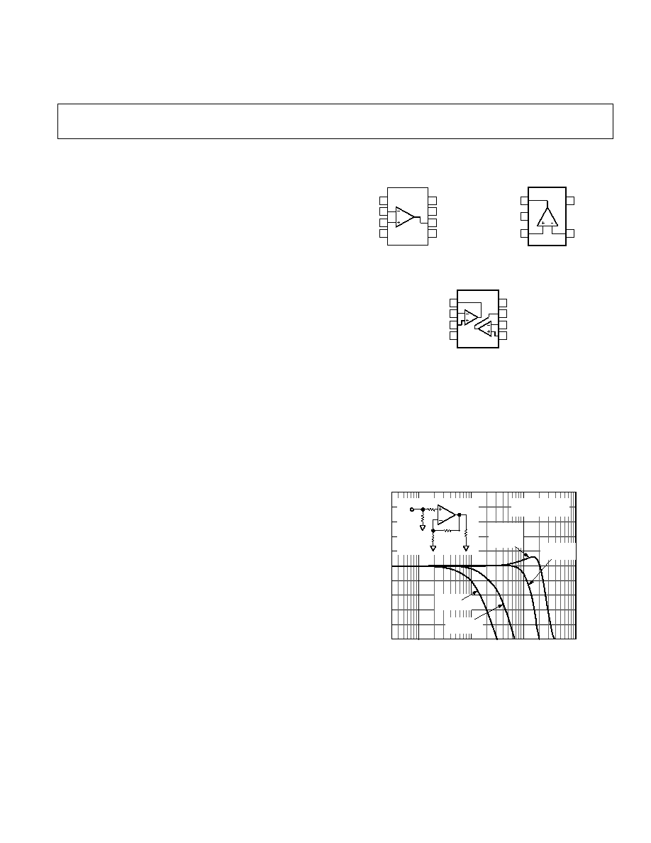
FREQUENCY ≠ Hz
0.3M
1G
GAIN ≠ dB
1M
10M
100M
5
4
≠5
3
2
1
0
≠1
≠2
≠3
≠4
G = +1
R
F
= 0
R
C
= 100
G = +2
R
F
= 402
G = +5
R
F
= 1000
G = +10
R
F
= 909
V
OUT
= 100mV p-p
R
L
= 100
V
IN
R
C
50
R
S
R
F
R
L
V
OUT
Figure 1. Frequency Response
N-8 and SO-8
1
2
3
4
8
7
6
5
(Not to Scale)
AD8055
≠IN
≠V
S
+IN
+V
S
V
OUT
NC
NC
NC
NC = NO CONNECT
SOT-23-5 (RT)
1
2
3
5
4
(Not to Scale)
≠IN
+IN
+V
S
V
OUT
AD8055
≠V
S
N-8, SO-8, microSOIC (RM)
1
2
3
4
8
7
6
5
(Not to Scale)
AD8056
≠IN1
≠V
S
+IN1
+V
S
OUT
≠IN2
OUT1
+IN2

≠2≠
REV. B
AD8055/AD8056≠SPECIFICATIONS
(@ T
A
= +25 C, V
S
= 65 V, R
F
= 402
, R
L
= 100
, Gain = +2,
unless otherwise noted)
Model
AD8055A/AD8056A
Conditions
Min
Typ
Max
Unit
DYNAMIC PERFORMANCE
≠3 dB Bandwidth
G = +1, V
O
= 0.1 V p-p
220
300
MHz
G = +1, V
O
= 2 V p-p
125
150
MHz
G = +2, V
O
= 0.1 V p-p
120
160
MHz
G = +2, V
O
= 2 V p-p
125
150
MHz
Bandwidth for 0.1 dB Flatness
V
O
= 100 mV p-p
25
40
MHz
Slew Rate
G = +1, V
O
= 4 V Step
1000
1400
V/
µs
G = +2, V
O
= 4 V Step
750
840
V/
µs
Settling Time to 0.1%
G = +2, V
O
= 2 V Step
20
ns
Rise and Fall Time, 10% to 90%
G = +1, V
O
= 0.5 V Step
2
ns
G = +1, V
O
= 4 V Step
2.7
ns
G = +2, V
O
= 0.5 V Step
2.8
ns
G = +2, V
O
= 4 V Step
4
ns
NOISE/HARMONIC PERFORMANCE
Total Harmonic Distortion
f
C
= 10 MHz, V
O
= 2 V p-p, R
L
= 1 k
≠72
dBc
f
C
= 20 MHz, V
O
= 2 V p-p, R
L
= 1 k
≠57
dBc
Crosstalk, Output to Output (AD8056)
f = 5 MHz, G = +2
≠60
dB
Input Voltage Noise
f = 100 kHz
6
nV/
Hz
Input Current Noise
f = 100 kHz
1
pA/
Hz
Differential Gain Error
NTSC, G = +2, R
L
= 150
0.01
%
NTSC, G = +2,
R
L
= 37.5
0.02
%
Differential Phase Error
NTSC, G = +2, R
L
= 150
0.02
Degree
NTSC, G = +2,
R
L
= 37.5
0.1
Degree
DC PERFORMANCE
Input Offset Voltage
3
5
mV
T
MIN
≠T
MAX
10
mV
Offset Drift
6
µV/∞C
Input Bias Current
0.4
1.2
µA
T
MIN
≠T
MAX
1
µA
Open Loop Gain
V
O
=
±2.5 V
66
71
dB
T
MIN
≠T
MAX
64
dB
INPUT CHARACTERISTICS
Input Resistance
10
M
Input Capacitance
2
pF
Input Common-Mode Voltage Range
3.2
±V
Common-Mode Rejection Ratio
V
CM
=
±2.5 V
82
dB
OUTPUT CHARACTERISTICS
Output Voltage Swing
R
L
= 150
2.9
3.1
±V
Output Current
1
V
O
=
±2.0 V
55
60
mA
Short Circuit Current
1
110
mA
POWER SUPPLY
Operating Range
±4.0
±5.0
±6.0
V
Quiescent Current
AD8055
5.4
6.5
mA
T
MIN
≠T
MAX
7.3
mA
AD8056
10
12
mA
T
MIN
≠T
MAX
13.3
mA
Power Supply Rejection Ratio
+V
S
= +5 V to +6 V, ≠V
S
= ≠5 V
66
72
dB
≠V
S
= ≠5 V to ≠6 V, +V
S
= +5 V
69
86
dB
OPERATING TEMPERATURE RANGE
≠40
+85
∞C
NOTES
1
Output current is limited by the maximum power dissipation in the package. See the power derating curves.
Specifications subject to change without notice.

AD8055/AD8056
≠3≠
REV. B
ABSOLUTE MAXIMUM RATINGS
1
Supply Voltage . . . . . . . . . . . . . . . . . . . . . . . . . . . . . . . 13.2 V
Internal Power Dissipation
2
Plastic DIP Package (N) . . . . . . . . . . . . . . . . . . . . . . 1.3 W
Small Outline Package (R) . . . . . . . . . . . . . . . . . . . . . 0.8 W
SOT-23-5 Package (RT) . . . . . . . . . . . . . . . . . . . . . . 0.5 W
microSOIC Package (RM) . . . . . . . . . . . . . . . . . . . . . 0.6 W
Input Voltage (Common Mode) . . . . . . . . . . . . . . . . . . .
±V
S
Differential Input Voltage . . . . . . . . . . . . . . . . . . . . . .
±2.5 V
Output Short Circuit Duration
. . . . . . . . . . . . . . . . . . . . . . Observe Power Derating Curves
Storage Temperature Range N, R . . . . . . . . ≠65
∞C to +125∞C
Operating Temperature Range (A Grade) . . ≠40
∞C to +85∞C
Lead Temperature Range (Soldering 10 sec) . . . . . . . +300
∞C
NOTES
1
Stresses above those listed under Absolute Maximum Ratings may cause perma-
nent damage to the device. This is a stress rating only; functional operation of the
device at these or any other conditions above those indicated in the operational
section of this specification is not implied. Exposure to absolute maximum rating
conditions for extended periods may affect device reliability.
2
Specification is for device in free air:
8-Lead Plastic DIP Package:
JA
= 90
∞C/W
8-Lead SOIC Package:
JA
= 155
∞C/W
5-Lead SOT-23-5 Package:
JA
= 240
∞C/W
8-Lead microSOIC Package:
JA
= 200
∞C/W
MAXIMUM POWER DISSIPATION
The maximum power that can be safely dissipated by the AD8055/
AD8056 is limited by the associated rise in junction temperature.
The maximum safe junction temperature for plastic encapsu-
lated devices is determined by the glass transition temperature
of the plastic, approximately +150
∞C. Exceeding this limit tem-
porarily may cause a shift in parametric performance due to a
change in the stresses exerted on the die by the package. Exceeding
a junction temperature of +175
∞C for an extended period can
result in device failure.
While the AD8055/AD8056 are internally short circuit protected,
this may not be sufficient to guarantee that the maximum junc-
tion temperature (+150
∞C) is not exceeded under all conditions.
To ensure proper operation, it is necessary to observe the maxi-
mum power derating curves.
AMBIENT TEMPERATURE ≠ C
≠50
0
T
J
= +150 C
2.0
1.5
1.0
0.5
MAXIMUM POWER DISSIPATION
≠
Watts
8-LEAD SOIC
PACKAGE
≠40 ≠30 ≠20 ≠10
0
10
20
30
40
50
60
70
80
90
8-LEAD PLASTIC DIP PACKAGE
SOIC
SOT-23-5
Figure 2. Plot of Maximum Power Dissipation vs.
Temperature for AD8055/AD8056
CAUTION
ESD (electrostatic discharge) sensitive device. Electrostatic charges as high as 4000 V readily
accumulate on the human body and test equipment and can discharge without detection.
Although the AD8055/AD8056 features proprietary ESD protection circuitry, permanent dam-
age may occur on devices subjected to high-energy electrostatic discharges. Therefore, proper
ESD precautions are recommended to avoid performance degradation or loss of functionality.
WARNING!
ESD SENSITIVE DEVICE
ORDERING GUIDE
Model
Temperature Range
Package Description
Package Option
Brand Code
AD8055AN
≠40
∞C to +85∞C
Plastic DIP
N-8
AD8055AR
≠40
∞C to +85∞C
Small Outline Package (SOIC)
SO-8
AD8055AR-REEL
≠40
∞C to +85∞C
13" Tape and Reel
SO-8
AD8055AR-REEL7
≠40
∞C to +85∞C
7" Tape and Reel
SO-8
AD8055ART-REEL
≠40
∞C to +85∞C
13" Tape and Reel
RT-5
H3A
AD8055ART-REEL7
≠40
∞C to +85∞C
7" Tape and Reel
RT-5
H3A
AD8056AN
≠40
∞C to +85∞C
Plastic DIP
N-8
AD8056AR
≠40
∞C to +85∞C
Small Outline Package (SOIC)
SO-8
AD8056AR-REEL
≠40
∞C to +85∞C
13" Tape and Reel
SO-8
AD8056AR-REEL7
≠40
∞C to +85∞C
7" Tape and Reel
SO-8
AD8056ARM
≠40
∞C to +85∞C
microSOIC
RM-8
H5A
AD8056ARM-REEL
≠40
∞C to +85∞C
13" Tape and Reel
RM-8
H5A
AD8056ARM-REEL7
≠40
∞C to +85∞C
7" Tape and Reel
RM-8
H5A

AD8055/AD8056
≠4≠
REV. B
≠Typical Performance Characteristics
V
IN
50
HP8130A
PULSE
GENERATOR
T
R
/T
F
= 1ns
AD8055
V
OUT
4.7 F
0.01 F
0.001 F
4.7 F
0.01 F
0.001 F
+V
S
≠V
S
6
7
2
3
4
100
100
Figure 3. Test Circuit, G = +1, R
L
= 100
Figure 4. Small Step Response, G = +1
Figure 5. Large Step Response, G = +1
HP8130A
PULSE
GENERATOR
T
R
/T
F
= 0.67ns
V
IN
57
AD8055
V
OUT
4.7 F
0.01 F
0.001 F
4.7 F
0.01 F
0.001 F
+V
S
≠V
S
402
402
6
7
2
3
4
100
Figure 6. Test Circuit, G = ≠1, R
L
= 100
Figure 7. Small Step Response, G = ≠1
Figure 8. Large Step Response, G = ≠1

AD8055/AD8056
≠5≠
REV. B
FREQUENCY ≠ Hz
0.3M
1G
GAIN
≠
dB
1M
10M
100M
5
4
≠5
3
2
1
0
≠1
≠2
≠3
≠4
G = +1
R
F
= 0
R
C
= 100
G = +2
R
F
= 402
G = +5
R
F
= 1000
G = +10
R
F
= 909
V
OUT
= 100mV p-p
R
L
= 100
V
IN
R
C
50
R
S
R
F
R
L
V
OUT
Figure 9. Small Signal Frequency Response,
G = +1, G = +2, G = +5, G = +10
FREQUENCY ≠ Hz
0.3M
1G
GAIN
≠
dB
1M
10M
100M
G = +1
R
F
= 0
G = +2
R
F
= 402
G = +5
R
F
= 1000
G = +10
R
F
= 909
V
OUT
= 2V p-p
R
L
= 100
5
4
≠5
3
2
1
0
≠1
≠2
≠3
≠4
Figure 10. Large Signal Frequency Response,
G = +1, G = +2, G = +5, G = +10
FREQUENCY ≠ Hz
0.3M
1G
1M
10M
100M
0.5
0.4
≠0.5
0.3
0.2
0.1
0
≠0.1
≠0.2
≠0.3
≠0.4
V
OUT
= 100mV
G = +2
R
L
= 100
R
F
= 402
OUTPUT
≠
dB
Figure 11. 0.1 dB Flatness
FREQUENCY ≠ Hz
10k
10M
100k
1M
V
OUT
= 2V p-p
G = +2
R
L
= 100
2ND
3RD
≠50
≠100
≠60
≠70
≠80
≠90
100M
HARMONIC DISTORTION
≠
dBc
Figure 12. Distortion vs. Frequency
FREQUENCY ≠ Hz
10k
10M
100k
1M
V
OUT
= 2V p-p
G = +2
R
L
= 1k
2ND
3RD
≠50
≠100
≠60
≠70
≠80
≠90
100M
DISTORTION
≠
dBc
Figure 13. Distortion vs. Frequency
V
OUT
≠ V p-p
0
1.2
0.4
0.8
G = +2
R
L
= 1k
2ND
3RD
≠50
≠90
≠60
≠70
≠80
1.6
DISTORTION
≠
dBc
2.0
2.4
2.8
3.2
3.6
4.0
≠40
Figure 14. Distortion vs. V
OUT
@ 20 MHz