 | ÐлекÑÑоннÑй компоненÑ: AD8075 | СкаÑаÑÑ:  PDF PDF  ZIP ZIP |
Äîêóìåíòàöèÿ è îïèñàíèÿ www.docs.chipfind.ru
REV. A
Information furnished by Analog Devices is believed to be accurate and
reliable. However, no responsibility is assumed by Analog Devices for its
use, nor for any infringements of patents or other rights of third parties that
may result from its use. No license is granted by implication or otherwise
under any patent or patent rights of Analog Devices.
a
AD8074/AD8075
One Technology Way, P.O. Box 9106, Norwood, MA 02062-9106, U.S.A.
Tel: 781/329-4700
www.analog.com
Fax: 781/326-8703
© Analog Devices, Inc., 2001
500 MHz, G = +1 and +2 Triple
Video Buffers with Disable
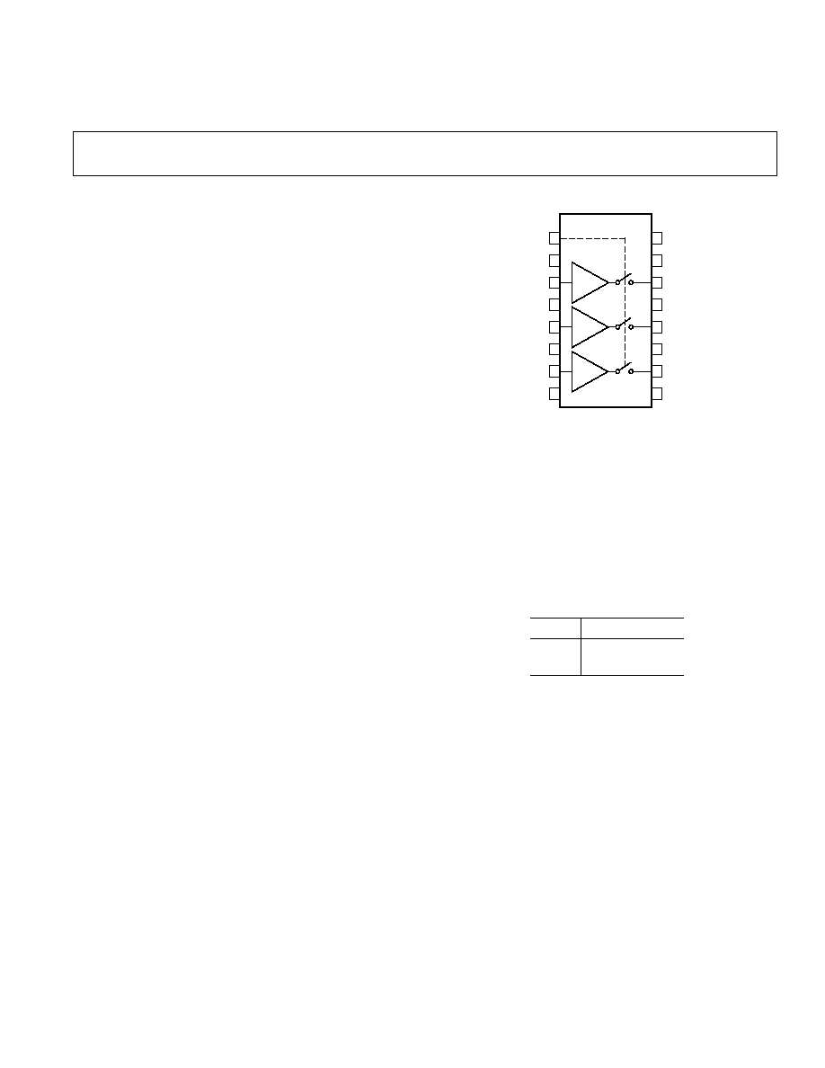
FUNCTIONAL BLOCK DIAGRAM
OE
DGND
IN2
AGND
IN1
AGND
IN0
V
EE
V
CC
V
CC
OUT2
V
EE
OUT1
V
CC
OUT0
V
EE
AD8074 /AD8075
1
2
3
4
5
6
7
8
16
15
14
13
12
11
10
9
G =
+1/+2
G =
+1/+2
G =
+1/+2
FEATURES
Dual Supply 5 V
High-Speed Fully Buffered Inputs and Outputs
600 MHz Bandwidth (3 dB) 200 mV p-p
500 MHz Bandwidth (3 dB) 2 V p-p
1600 V/ s Slew Rate, G = +1
1350 V/ s Slew Rate, G = +2
Fast Settling Time: 4 ns
Low Supply Current: < 30 mA
Excellent Video Specifications (R
L
= 150 ):
Gain Flatness of 0.1 dB to 50 MHz
0.01% Differential Gain Error
0.01 Differential Phase Error
"All Hostile" Crosstalk
80 dB @ 10 MHz
50 dB @ 100 MHz
High "OFF" Isolation of 90 dB @ 10 MHz
Low Cost
Fast Output Disable Feature
APPLICATIONS
RGB Buffer in LCD and Plasma Displays
RGB Driver
Video Routers
PRODUCT DESCRIPTION
The AD8074/AD8075 are high-speed triple video buffers with
G = +1 and +2 respectively. They have a 3 dB full signal band-
width in excess of 450 MHz, along with slew rates in excess of
1400 V/
µs. With better than 80 dB of all hostile crosstalk and
90 dB isolation, they are useful in many high-speed applica-
tions. The differential gain and differential phase error are 0.01%
and 0.01
°. Gain flatness of 0.1 dB up to 50 MHz makes the
AD8074/AD8075 ideal for RGB buffering or driving. They
consume less than 30 mA on a
± 5 V supply.
Both devices offer a high-speed disable feature that allows the
outputs to be put into a high impedance state. This allows the
building of larger input arrays while minimizing "OFF" chan-
nel output loading. The AD8074/AD8075 are offered in a
16-lead TSSOP package.
Table I. Truth Table
OE
OUT0, 1, 2
0
IN0, IN1, IN2
1
High Z

REV. A
2
AD8074/AD8075SPECIFICATIONS
(T
A
= 25 C, V
S
= 5 V, unless otherwise noted.)
Parameter
Conditions
Min
Typ
Max
Unit
DYNAMIC PERFORMANCE
3 dB Bandwidth (Small Signal)
V
IN
= 200 mV p-p, C
L
= 5 pF
330/310
600/550
MHz
V
IN
= 200 mV p-p, R
L
= 150
250/230
400/400
MHz
3 dB Bandwidth (Large Signal)
V
IN
= 2 V p-p, C
L
= 5 pF
330/300
500/500
MHz
V
IN
= 2 V p-p, R
L
= 150
250/230
350/350
MHz
0.1 dB Bandwidth
V
IN
= 200 mV p-p, C
L
= 5 pF
70/65
MHz
V
IN
= 200 mV p-p, R
L
= 150
70/65
MHz
Slew Rate
2 V Step, R
L
= 1 k
/150
1600/1350
V/
µs
Settling Time to 0.1%
2 V Step, R
L
= 1 k
/150
4/7.5
ns
NOISE/DISTORTION PERFORMANCE
Differential Gain
V
= 3.58 MHz, 150
0.01
%
Differential Phase
V
= 3.58 MHz, 150
0.01
Degrees
All Hostile Crosstalk
V
= 10 MHz, R
L
= 1 k
80/74
dB
V
= 100 MHz, R
L
= 1 k
50/44
dB
OFF Isolation
V
= 10 MHz, R
L
= 150
90
dB
Voltage Noise
V
= 10 kHz to 100 MHz
19.5/22
nV/
Hz
DC PERFORMANCE
Voltage Gain Error
No Load
±0.1/±0.2 ±0.15/±0.65 %
Input Offset Voltage
2.5
27/40
mV
T
MIN
to T
MAX
3
mV
Input Offset Drift
10
µV/°C
Input Bias Current
5
9.5/10
µA
INPUT CHARACTERISTICS
Input Resistance
10
M
Input Capacitance
Channel Enabled
1.5
pF
Channel Disabled
1.5
pF
Input Voltage Range
±2.8/±1.4
V
OUTPUT CHARACTERISTICS
Output Voltage Swing
R
L
= 1 k
+V
S
1.95
+V
S
1.8
V
V
S
+ 2.1
V
S
+ 1.8
V
R
L
= 150
+V
S
2.35
+V
S
2.2
V
V
S
+ 2.30
V
S
+ 2.2
V
Short Circuit Current (Protected)
70
mA
Output Resistance
Enabled
0.5
Disabled
3.5
7.5
M
Output Capacitance
Disabled
2.2
pF
POWER SUPPLY
Operating Range
±4.5
±5.5
V
Power Supply Rejection Ratio
+PSRR: +V
S
= +4.5 V to +5.5 V, V
S
= 5 V
60
74
dB
PSRR: V
S
= 4.5 V to 5.5 V, +V
S
= +5 V
56
64
dB
Quiescent Current
All Channels "ON"
21.5/24
30
mA
All Channels "OFF"
3/4
5.5
mA
T
MIN
to T
MAX
23/26
mA
DIGITAL INPUT
Logic "1" Voltage
OE Input
2.0
V
Logic "0" Voltage
OE Input
0.8
V
Logic "1" Input Current
OE = 4 V
100
nA
Logic "0" Input Current
OE = 0.4 V
1
µA
OPERATING TEMPERATURE RANGE
Temperature Range
Operating (Still Air)
40
+85
°C
JA
Operating (Still Air)
150.4
°C/W
JC
Operating
27.6
°C/W
Specifications subject to change without notice.
REV. A
AD8074/AD8075
3
ABSOLUTE MAXIMUM RATINGS
1
Supply Voltage . . . . . . . . . . . . . . . . . . . . . . . . . . . . . . . . . 12.0 V
Internal Power Dissipation
2, 3
AD8074/AD8075 16-Lead TSSOP (RU) . . . . . . . . . . . . . 1 W
Input Voltage
IN0, IN1, IN2 . . . . . . . . . . . . . . . . . . . . . . . . . V
EE
V
IN
V
CC
OE . . . . . . . . . . . . . . . . . . . . . . . . . . . . . DGND
V
IN
V
CC
Output Short Circuit Duration . . . . . . . . . . . . . . . . . . Indefinite
3
Storage Temperature Range . . . . . . . . . . . . . . 65
°C to +150°C
Lead Temperature Range (Soldering 10 sec) . . . . . . . . . . . 300
°C
NOTES
1
Stresses above those listed under Absolute Maximum Ratings may cause perma-
nent damage to the device. This is a stress rating only; functional operation of the
device at these or any other conditions above those indicated in the operational
section of this specification is not implied. Exposure to absolute maximum rating
conditions for extended periods may affect device reliability.
2
Specification is for device in free air (T
A
= 25
°C).
3
16-lead plastic TSSOP;
JA
= 150.4
°C/W. Maximum internal power dissipa-
tion (P
D
) should be derated for ambient temperature (T
A
) such that
P
D
< (150
°C T
A
)/
JA
.
ORDERING GUIDE
Temperature
Package
Package
Model
Range
Description
Option
AD8074ARU
40
°C to +85°C 16-Lead Plastic TSSOP RU-16
AD8075ARU
40
°C to +85°C 16-Lead Plastic TSSOP RU-16
AD8074-EVAL
Evaluation Board
AD8075-EVAL
Evaluation Board
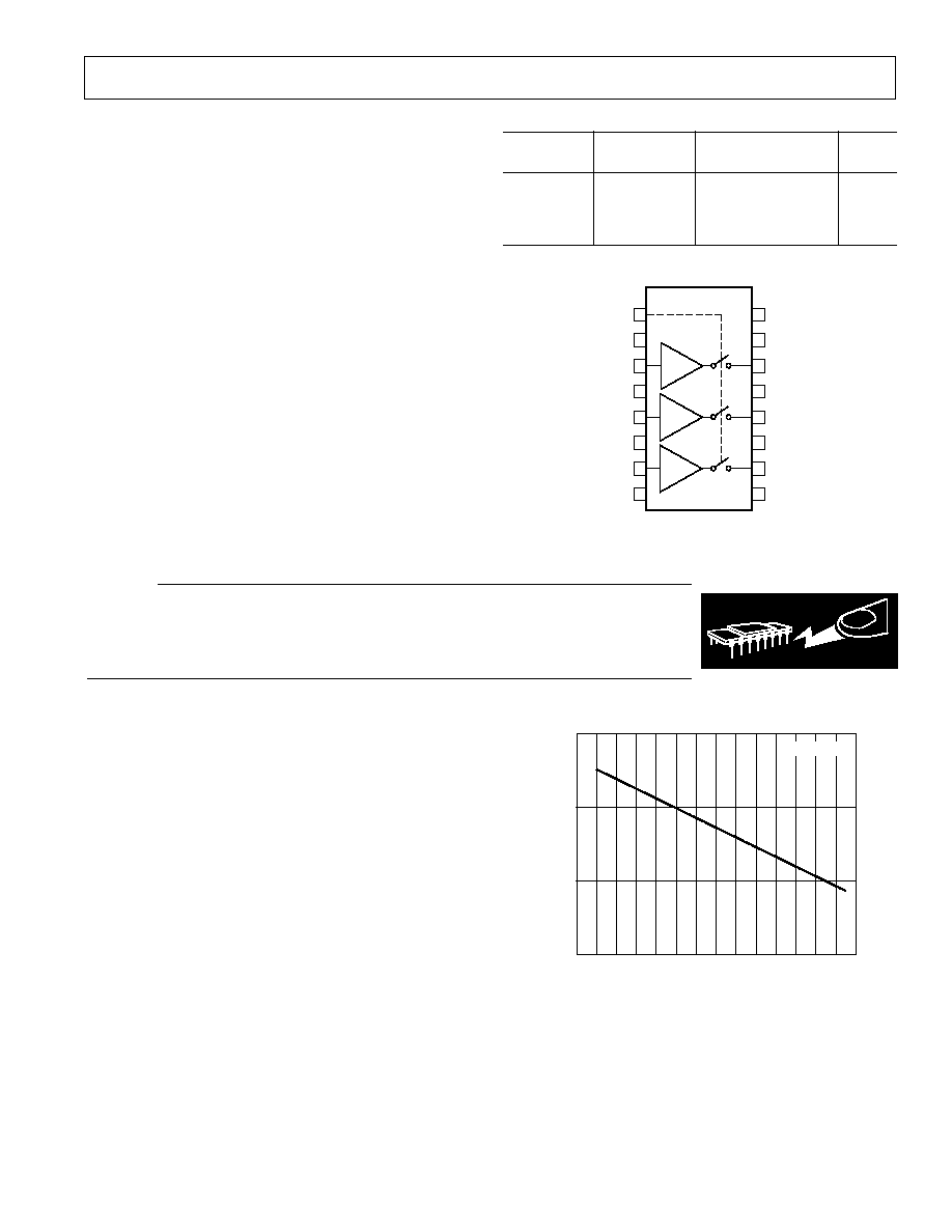
PIN CONFIGURATION
OE
DGND
IN2
AGND
IN1
AGND
IN0
V
EE
V
CC
V
CC
OUT2
V
EE
OUT1
V
CC
OUT0
V
EE
AD8074 /AD8075
1
2
3
4
5
6
7
8
16
15
14
13
12
11
10
9
G =
+1/+2
G =
+1/+2
G =
+1/+2
MAXIMUM POWER DISSIPATION
The maximum power that can be safely dissipated by the AD8074/
AD8075 is limited by the associated rise in junction temperature.
The maximum safe junction temperature for plastic encapsulated
devices is determined by the glass transition temperature of the
plastic, approximately 150
°C. Temporarily exceeding this limit
may cause a shift in parametric performance due to a change in
the stresses exerted on the die by the package. Exceeding a junc-
tion temperature of 175
°C for an extended period can result in
device failure.
While the AD8074/AD8075 is internally short circuit protected,
this may not be sufficient to guarantee that the maximum junction
temperature (150
°C) is not exceeded under all conditions. To
ensure proper operation, it is necessary to observe the maximum
power derating curves shown in Figure 1.
WARNING!
ESD SENSITIVE DEVICE
CAUTION
ESD (electrostatic discharge) sensitive device. Electrostatic charges as high as 4000 V readily
accumulate on the human body and test equipment and can discharge without detection. Although
the AD8074/AD8075 features proprietary ESD protection circuitry, permanent damage may occur
on devices subjected to high-energy electrostatic discharges. Therefore, proper ESD precautions
are recommended to avoid performance degradation or loss of functionality.
AMBIENT TEMPERATURE C
MAXIMUM POWER DISSIPATION Watts
T
J
= 150 C
0
10
30
50
70
90
0
0.5
1.0
1.5
50
30
10
Figure 1. Maximum Power Dissipation vs. Temperature
REV. A
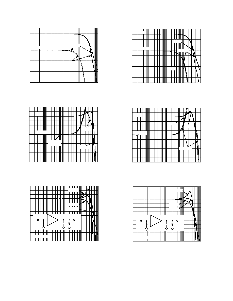
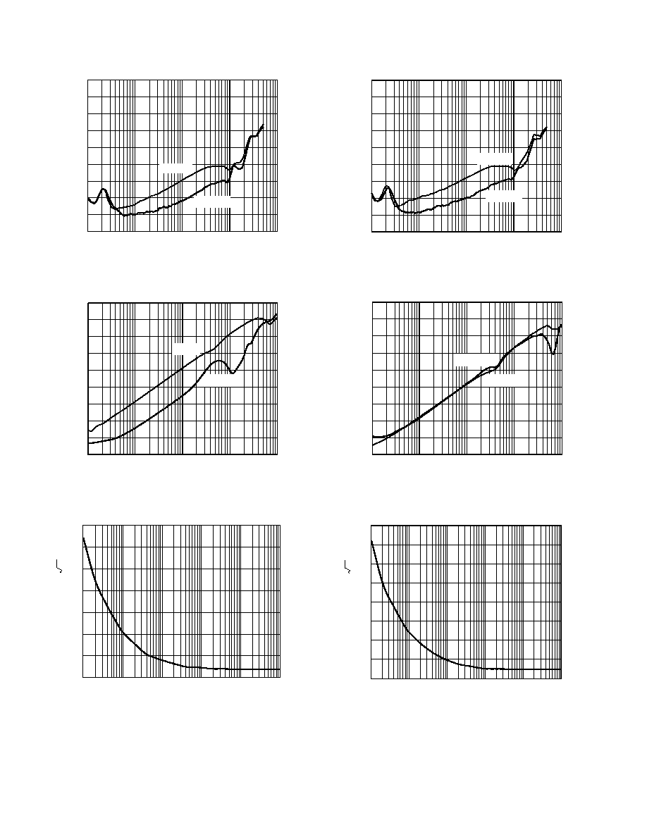
AD8074/AD8075Typical Performance Characteristics
4
GAIN
2V p-p
200mV p-p
FREQUENCY MHz
GAIN
dB
0.1
1000
1
10
100
1
0
1
2
3
4
5
6
7
8
9
0.4
0.3
0.2
0.1
0
0.1
0.2
0.3
0.4
0.5
0.6
FLA
TNESS
dB
FLATNESS
TPC 1. AD8074 Frequency Response; R
L
= 150
GAIN
dB
0.1
1000
1
10
100
2
1
0
1
2
3
4
5
6
7
8
9
10
0.6
0.5
0.4
0.3
0.2
0.1
0
0.1
0.2
0.3
0.4
0.5
0.6
FLA
TNESS
dB
200mV p-p
2V p-p
GAIN
FLATNESS
FREQUENCY MHz
200mV p-p
2V p-p
TPC 2. AD8074 Frequency Response; R
L
= 1 k
, C
L
= 5 pF
GAIN
dB
3
2
1
0
1
2
3
4
5
6
7
8
9
10
0.1 1 10 100 1000
FREQUENCY MHz
V
OUT
= 2V p-p
C
L
= 10pF
C
L
= 0pF
C
L
= 5pF
V
IN
V
OUT
C
L
1k
75
TPC 3. AD8074 Frequency Response vs. Capacitive Load
FLATNESS
GAIN
2V p-p
200mV p-p
2V p-p
FREQUENCY MHz
0.1
1000
1
10
100
1
0
1
2
3
4
5
6
7
8
9
0.4
0.3
0.2
0.1
0
0.1
0.2
0.3
0.4
0.5
0.6
NORMALIZED FLA
TNESS
dB
NORMALIZED GAIN
dB
TPC 4. AD8075 Frequency Response; R
L
= 150
0.1
1000
1
10
100
2
1
0
1
2
3
4
5
6
7
8
9
10
0.6
0.5
0.4
0.3
0.2
0.1
0
0.1
0.2
0.3
0.4
0.5
0.6
2V p-p
GAIN
FLATNESS
NORMALIZED FLA
TNESS
dB
NORMALIZED GAIN
dB
200mV p-p
FREQUENCY MHz
2V p-p
TPC 5. AD8075 Frequency Response; R
L
= 1 k
, C
L
= 5 pF
N
ORMALIZED GAIN
dB
3
2
1
0
1
2
3
4
5
6
7
8
9
10
0.1 1 10 100 1000
FREQUENCY MHz
V
OUT
= 2V p-p
C
L
= 10pF
C
L
= 0pF
C
L
= 5pF
V
IN
V
OUT
C
L
150k
75
TPC 6. AD8075 Frequency Response vs. Capacitive Load
REV. A
AD8074/AD8075
5
FREQUENCY MHz
0
0.1
1000
1
10
100
10
20
30
40
50
60
70
80
90
100
110
V
OUT
= 2V p-p (ACTIVE CHANNEL(s))
R
L
= 1k
R
T
= 37.5
ALL-HOSTILE
ADJACENT
CR
OSST
ALK
dB
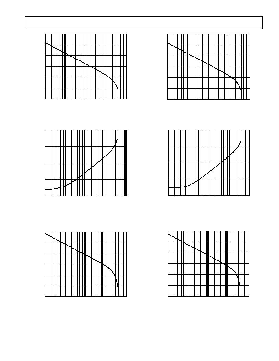
TPC 7. AD8074 Crosstalk vs. Frequency (All Hostile and
Adjacent R
L
= 1 k
)
FUNDAMENTAL FREQUENCY MHz
0
1
1000
10
100
10
20
30
40
50
60
70
80
90
100
V
OUT
= 2V p-p
R
L
= 150
R
T
= 37.5
THIRD
HARMONIC
SECOND
HARMONIC
DIST
O
R
T
ION
dBc
TPC 8. AD8074 Distortion vs. Frequency
FREQUENCY MHz
0
0.1
1000
1
10
100
10
20
30
40
50
60
70
80
90
100
110
V
OUT
= 2V p-p (ACTIVE CHANNEL(s))
R
L
= 150
R
T
= 37.5
ALL-HOSTILE
ADJACENT
CR
OSST
ALK
dB
TPC 9. AD8075 Crosstalk vs. Frequency (All Hostile and
Adjacent R
L
= 150
)
FUNDAMENTAL FREQUENCY MHz
0
1
1000
10
100
10
20
30
40
50
60
70
80
90
100
SECOND
HARMONIC
THIRD
HARMONIC
V
OUT
= 2V p-p
R
L
= 150
R
T
= 37.5
DIST
O
R
T
ION
dBc
TPC 10. AD8075 Distortion vs. Frequency
REV. A
AD8074/AD8075
6
FREQUENCY MHz
0.1
1000
1
10
100
20
30
40
50
60
70
80
90
100
110
R
L
= 1k
R
L
= 150
OFF ISOLA
T
ION
dB
TPC 11. AD8074 Off Isolation vs. Frequency
FREQUENCY MHz
0.1
1000
1
10
100
20
30
40
50
60
70
80
10
0
10
+PSRR
PSRR
PSRR
dB
TPC 12. AD8074 PSRR vs. Frequency
V
O
L
T
A
GE NOISE
nV/ Hz
10
100
1M
1k
10k
100k
FREQUENCY Hz
350
300
250
200
150
100
50
0
TPC 13. AD8074 Voltage Noise vs. Frequency
FREQUENCY MHz
0.1
1000
1
10
100
20
30
40
50
60
70
80
90
100
110
R
L
= 1k
R
L
= 150
OFF ISOLA
T
ION
dB
TPC 14. AD8075 Off Isolation vs. Frequency
FREQUENCY MHz
0.1
1000
1
10
100
10
20
30
40
50
60
70
20
10
0
+PSRR
PSRR
PSRR
dB
TPC 15. AD8075 PSRR vs. Frequency
10
100
1M
1k
10k
100k
V
O
L
T
A
GE NOISE
nV/ Hz
FREQUENCY Hz
350
300
250
200
150
100
50
0
400
TPC 16. AD8075 Voltage Noise vs. Frequency
REV. A
AD8074/AD8075
7
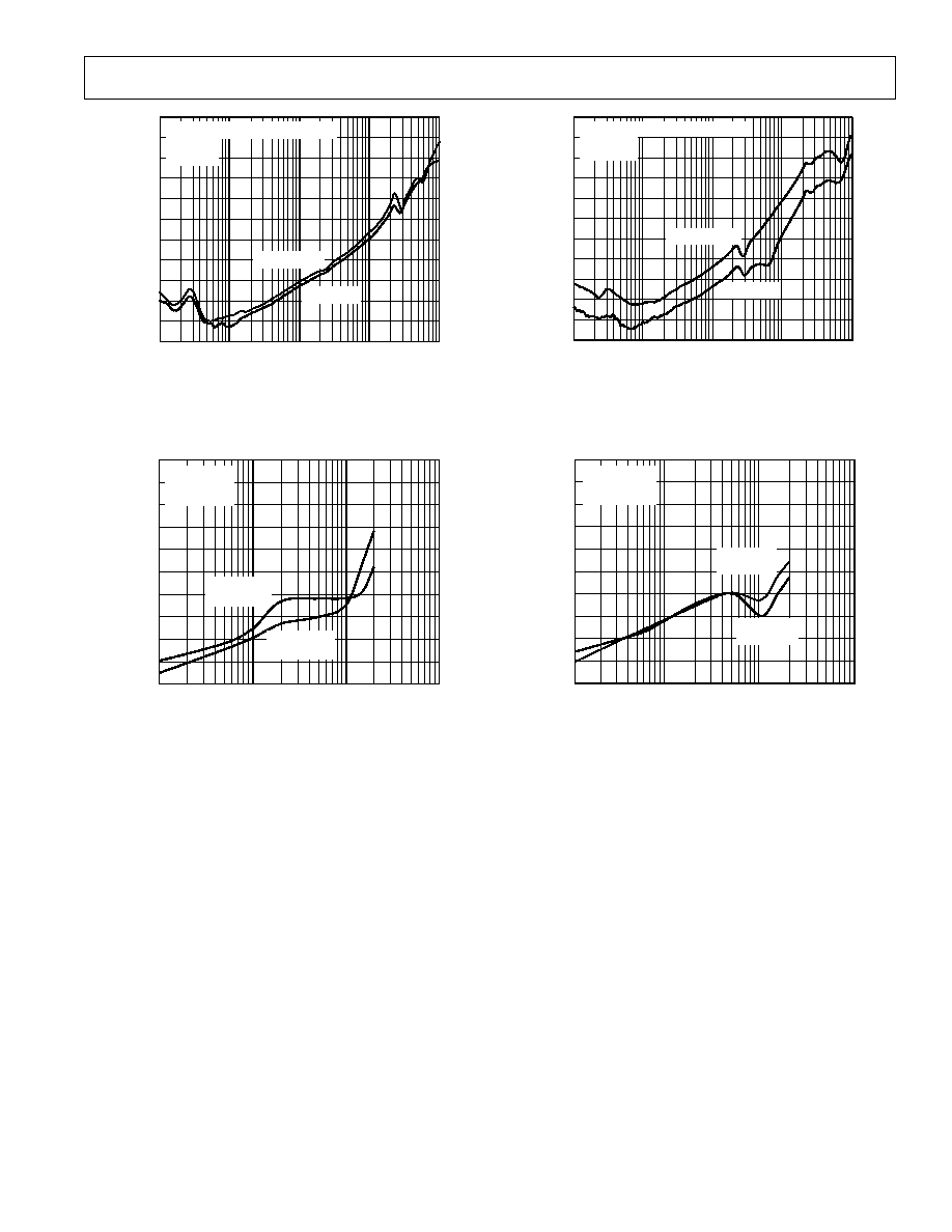
FREQUENCY MHz
0.1
1000
1
10
100
10000
1000
100
10
1
0.1
0.01
INPUT IMPED
ANCE
k
TPC 17. AD8074 Input Impedance vs. Frequency
FREQUENCY MHz
0.1
1000
1
10
100
1000
100
10
1
0.1
OUTPUT IMPED
ANCE
TPC 18. AD8074 Output Impedance vs. Frequency;
Enabled
FREQUENCY MHz
0.1
1000
1
10
100
0.001
1000
100
10
1
0.1
0.01
OUTPUT IMPED
ANCE
k
TPC 19. AD8074 Output Impedance vs. Frequency;
Disabled
FREQUENCY MHz
0.1
1000
1
10
100
10000
1000
100
10
1
0.1
0.01
INPUT IMPED
ANCE
k
TPC 20. AD8075 Input Impedance vs. Frequency
FREQUENCY MHz
0.1
1000
1
10
100
1000
100
10
1
0.1
OUTPUT IMPED
ANCE
TPC 21. AD8075 Output Impedance vs. Frequency;
Enabled
FREQUENCY MHz
0.1
1000
1
10
100
0.001
1000
100
10
1
0.1
0.01
OUTPUT IMPED
ANCE
k
TPC 22. AD8075 Output Impedance vs. Frequency;
Disabled
REV. A
AD8074/AD8075
8
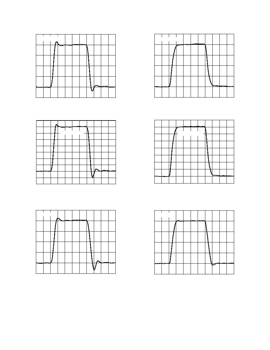
2ns
V
O
= 200mV STEP
0
0.15
0.10
0.05
0.05
0.10
0.15
TPC 23. AD8074 Small Signal Pulse Response (R
L
= 1 k
,
C
L
= 5 pF)
0
0.2
0.1
0.6
0.1
0.2
0.3
0.4
0.5
0.7
0.8
2ns
V
O
= 700mV STEP
TPC 24. AD8074 Video Amplitude Pulse Response
(R
L
= 1 k
, C
L
= 5 pF)
0
1.5
1.0
1.5
0.5
1.0
0.5
2ns
V
O
= 2V STEP
TPC 25. AD8074 Large Signal Pulse Response
(R
L
= 1 k
, C
L
= 5 pF)
0
0.15
0.10
0.15
0.05
0.10
0.05
2ns
V
O
= 200mV STEP
TPC 26. AD8075 Small Signal Pulse Response (R
L
= 150 k
)
2ns
0.1
0
0.1
0.2
0.3
0.4
0.5
0.6
0.7
0.8
V
O
= 700mV STEP
TPC 27. AD8075 Video Amplitude Pulse Response
(R
L
= 150
)
1.5
0
0.5
1.0
1.5
1.0
0.5
2ns
V
O
= 2V STEP
TPC 28. AD8075 Large Signal Pulse Response (R
L
= 150
)
REV. A
AD8074/AD8075
9
THEORY OF OPERATION
The AD8074 (G = +1) and AD8075 (G = +2) are triple-channel,
high-speed buffers with TTL-compatible output enable control.
Optimized for buffering RGB (red, green, blue) video sources,
the devices have high peak slew rates, maintaining their band-
width for large signals. Additionally, the buffers are compensated
for high phase margin, minimizing overshoot for good pixel
resolution. The buffers also have video specifications that are
suitable for buffering NTSC or PAL composite signals.
The buffers are organized as three independent channels, each
with an input transconductance stage and an output trans-
impedance stage. Each channel is characterized by low input
capacitance and high input impedance. The transconductance
stages, NPN differential pairs, source signal current into the folded
cascode output stages. Each output stage contains a compensat-
ing network and emitter follower output buffer. Internal voltage
feedback sets the gain, the AD8074 being configured as a unity
gain follower, and the AD8075 as a gain-of-two amplifier with a
feedback network. The architecture provides drive for a reverse-
terminated video load (150
) with low differential gain and
phase error for relatively low power consumption. Careful chip
design and layout allow excellent crosstalk isolation between
channels.
One logic pin,
OE, controls whether the three outputs are
enabled, or disabled to a high-impedance state. The high imped-
ance disable allows larger matrices to be built when busing the
outputs together. When disabled, the AD8074 and AD8075 con-
sume a fifth the power as when enabled. In the case of the
AD8075 (G = +2), a feedback isolation scheme is used so that
the impedance of the gain-of-two feedback network does not
load the output.
Full power bandwidth for an undistorted sinusoid is often calcu-
lated using peak slew rate from the equation:
Full Power Bandwidth
Peak Slew Rate
Sinusoidal Amplitude
=
× ×
2
Peak slew rate is not the same as average slew rate (25% to
75%) which is typically specified. For a natural response, peak
slew rate may be 2.7 times larger than average slew rate. There-
fore, calculating a full power bandwidth with a specified average
slew rate will give a pessimistic result.
The primary cause of overshoot in these amplifiers is the pres-
ence of large reactive loads at the output and insufficient series
isolation of the load. However, it is possible to overdrive these
amplifiers with 1 V, subnanosecond input-pulse edges. The
ensuing dynamics may give rise to subnanosecond overshoot. To
reduce these effects, an edge-rate limiting network at the input
should be considered for input transition times less than 0.5 ns.
APPLICATIONS
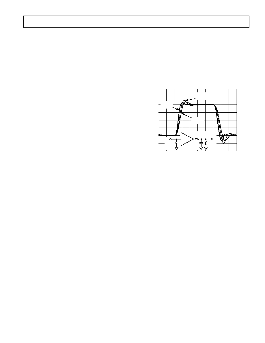
Response Tuning
It has been mentioned in passing that the primary cause of over-
shoot for the AD8074 and AD8075 is the presence of large
reactive loads at the output. If the system exhibits excessive
ringing while settling, a 10
50 series resistor may be used
at the output to isolate the emitter-follower output buffer from
the reactive load. If the output exhibits an overdamped response,
the system designer may add a few pF shunt capacitance at the
output to tune for a faster edge transition. A system with a small
degree of overshoot will settle faster than an overdamped system.
V
IN
V
OUT
R
S
C
L
1k
75
2ns
R
S
= 0
C
L
= 5pF
R
S
= 10
C
L
= 10pF
R
S
= 20
C
L
= 15pF
2.0
1.5
1.0
0.5
0
0.5
1.0
1.5
2.0
Figure 2. Driving Capacitive Loads
Single Supply Operation
The AD8074 and AD8075 may be operated from a single 10 V
supply. In this configuration, the AD8075's AGND pins must
be tied near midsupply, as AGND provides the reference for the
ground buffer, to which the internal gain network is terminated.
Logic is referenced to DGND. The buffers are disabled in single
supply operation for V
OE
> V
DGND
+ ~2.0 V and enabled for
V
OE
< V
DGND
+ 0.8 V. TTL logic levels are expected. The fol-
lowing restrictions are placed upon the digital ground potential:
3 5
12
.
V
V
V
V
AVCC
DGND
V
DGND
V
AVEE
The architecture of the output buffer is such that the output
voltage can swing to within ~2.3 V of either rail. For example, if
the output need swing only 2 V, then the buffers could be oper-
ated on dual 3.5 V or single 7 V supplies. It is cautioned that
saturation effects may become noticeable when the output swings
within 2.6 V of either rail. The system designer may opt to
use this characteristic to his or her advantage by using the
soft-saturation regime, (2.2 V2.6 V from the supply rails), to
tame excessive overshoot. The designer is cautioned that a
charge storage associated time delay of several nanoseconds is
incurred when recovering from soft-saturation. This effect
results in longer settling tails.
REV. A
AD8074/AD8075
10
RGB Buffer for Second Monitor
The RGB signals for PC monitors are driven through coax
cables whose characteristic impedance is 75
. The graphics
chip will generally have current-source output drivers that should
be double terminated with a 75
shunt termination at each end.
On the transmit end, the shunt terminations are provided to
ground close to the graphics IC, while the monitor terminates
its end via internal termination resistors. While this scheme works
well and is virtually foolproof for a single monitor, it leaves no
means for passively connecting a second monitor to the same source.
A second monitor that is connected simply in parallel will pro-
vide an extra set of terminations that will upset the signal levels.
To keep costs low, most computer monitors do not have the ability
to open-circuit the terminations in order that an additional monitor
can be connected to the same signal, as is done in some studio-
type TV monitors.
A way around this problem is to connect the first monitor to the
RGB channels in the standard fashion, and then to provide a
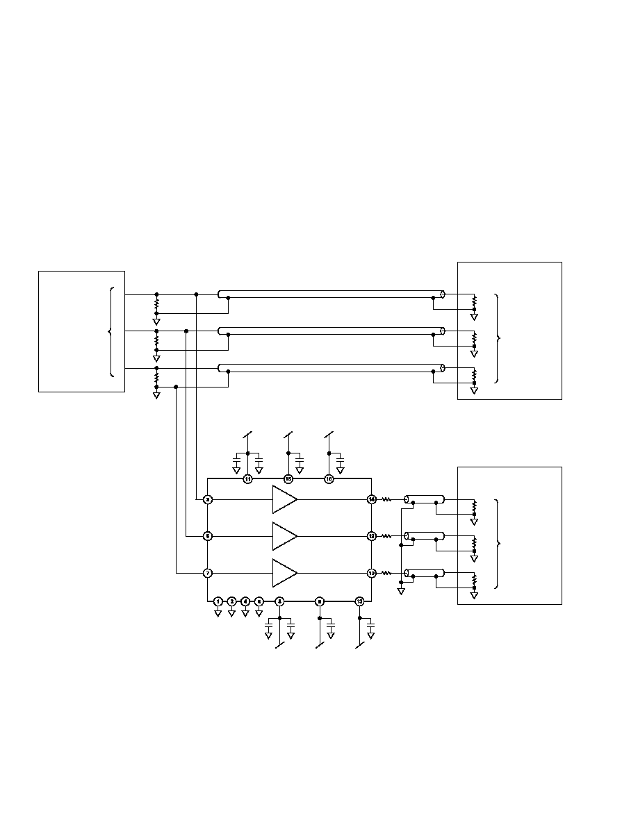
triple gain-of-two buffer to drive the second monitor. The AD8075
is designed to provide this function and also provide excellent
high-frequency performance for high-resolution graphics signals.
Figure 3 shows a schematic of this circuit.
The outputs of the AD8075 are low impedance voltage sources
and are therefore series-terminated with 75
resistors. The
internal resistors in Monitor #2 provide the terminations at its
end. The overall effect of this type of termination scheme is to
divide the signal amplitude by two. This is compensated by the
gain of two provided by the AD8075.
0.1 F
5V
0.1 F
5V
0.1 F
5V
+
25 F
0.1 F
+5V
0.1 F
+5V
0.1 F
+5V
+
25 F
AD8075
75
75
75
75
75
75
75
75
75
MONITOR #1
MONITOR #2
INTERNAL
TERMINATIONS
INTERNAL
TERMINATIONS
75
75
75
R
G
B
PC GRAPHICS IC
CURRENT SOURCE
OUTPUT DRIVERS
Figure 3. Buffer
REV. A
AD8074/AD8075
11
Triple Video Multiplexer
The AD8074 and AD8075 each have an output-enable function
that can be used to disable the outputs and put them in a high-
impedance state. Usually, for a unity-gain device, it is relatively
easy to provide high disabled impedance, because the feedback
path is from the output to a high-impedance input. However, for a
non-unity-gain part, the feedback provides a resistive path to
ground. This will usually dominate the disabled output imped-
ance, and make it a much lower value than the unity-gain device.
The AD8075 has an internal buffer that provides a low-impedance,
ground level output that terminates the feedback path during
enabled operation. In the disabled state, both this buffer output
and the amplifier output are disabled to a high impedance to
provide a high-impedance disabled state.
To construct a multiplexer, the outputs from one or more devices
are connected in parallel and only one device is enabled at a
time while all of the others are disabled. The two sets of inputs
are applied individually to each of the separate device inputs.
Figure 4 shows the circuit details for this function. The first RGB
Source 1 is input to the first AD8075. Each of the individual
signals is terminated to ground with 75
to provide proper
termination for the input cables. In a similar fashion, the Source
2 signals are input to the second AD8075.
0.1 F
5V
0.1 F
5V
0.1 F
5V
+
25 F
0.1 F
+5V
0.1 F
+5V
0.1 F
+5V
+
25 F
AD8075
75
75
75
OE
75
75
75
R
G
B
SOURCE 2
0.1 F
5V
0.1 F
5V
0.1 F
5V
+
25 F
0.1 F
+5V
0.1 F
+5V
0.1 F
+5V
+
25 F
AD8075
75
75
75
OE
75
75
75
R
G
B
SOURCE 1
SEL1/
SEL2
R
G
B
OUTPUT
Figure 4. Mux

REV. A
AD8074/AD8075
12
Each of the six outputs has a 75
series resistor that is used to
reverse-terminate the output transmission line. The correspond-
ing outputs are then wired in parallel and delivered to the output
cable. The termination resistors in this position help to isolate
the off capacitance of the disabled device's outputs from loading
the enabled device's outputs. The gain-of-two of the AD8075
compensates for the signal halving that occurs as a result of the
output terminations.
A select signal is provided directly to the
OE of the second
AD8075 and an inverted version is used to drive the other device's
OE. This will ensure that only one device is active at a time. Since
there is a total of 150
in series between any two outputs, it is
not essential to be overly concerned about the exact timing of
the making and breaking of the enable signals.
Additional inputs can easily be added to the circuit shown to
make wider multiplexers. The outputs of all of the devices will
be wired in parallel, and the logic must allow that only one output
be enabled at a time.
If it is desired to make a triple 3:1 multiplexer, a triple 2:1 mul-
tiplexer, like the AD8185 can be used along with the AD8075.
The same general guidelines for input and output treatment
should be followed and the logic must perform the proper function.
If it is desired to design such a multiplexer at unity gain, the
AD8074 should be used. For a triple 3:1 multiplexer, an
AD8183 (triple 2:1 mux) can be combined with an AD8074 to
provide this function.
Layout and Grounding
The AD8074 and AD8075 are extreme bandwidth, high-slew-rate
devices that are designed to drive up to the highest resolution
monitors and provide excellent resolution. To realize their full
performance potential, it is essential to adhere to the best prac-
tices of high-speed PCB layout.
A major area of focus should be the power distribution system.
There should be a full ground plane that provides the reference
and return paths for both the inputs and outputs. The ground
also provides isolation between the input signals to minimize the
crosstalk. This ground plane should cover as wide an area as
possible and be minimally interrupted in order to keep its
impedance to a minimum.
The power planes should also be as broad as possible to provide
minimal inductance, which is required for high-slew-rate sig-
nals. These power planes layers should be spaced closely to the
ground plane to increase the interplane capacitance between the
supplies and ground.
Each supply pin should be bypassed with a low inductance
0.1
µF ceramic capacitance with minimal excess circuit length
to minimize the series impedance. A 25
µF tantalum electro-
lytic capacitor will supply a charge reservoir for lower frequency,
high-amplitude transitions.
The input and output signals should be run as directly as pos-
sible in order to minimize the effects of parasitics. If they must
run over a longer distance of more than a few centimeters, con-
trolled impedance PCB traces should be used to minimize the
effect of reflections due to mismatches in impedance and the
proper termination should be provided.
To avoid excess crosstalk, the above recommendations should
be followed carefully. The power system and signal routing are
the most important aspects of preventing excess crosstalk.
Beyond these techniques, shielding can be provided by ground
traces between adjacent signals, especially those that travel
parallel over long distances.
REV. A
AD8074/AD8075
13
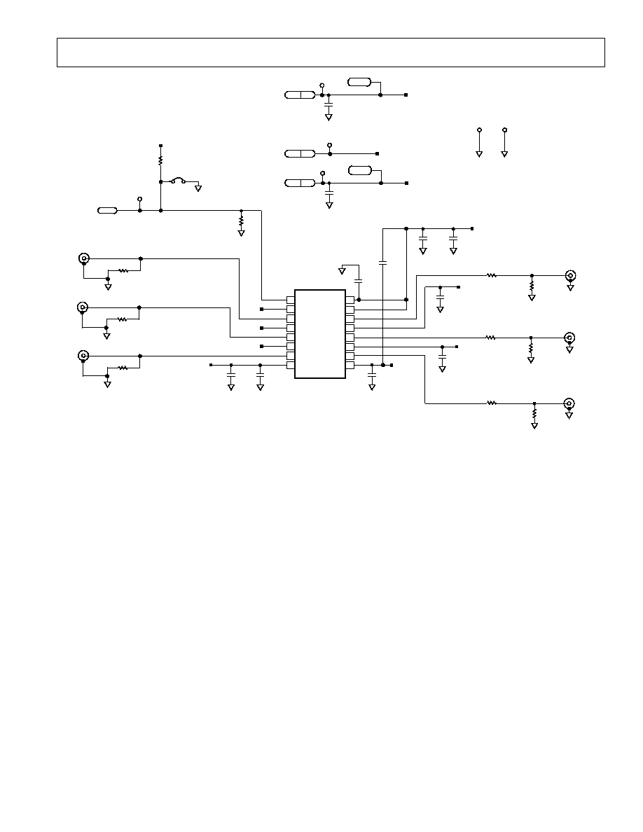
AGND
AGND
TP4
TP3
DO NOT INSTALL
AGND
AGND
AGND
DO NOT INSTALL
10 F
C2
C1
10 F
50 IMPEDANCE LINE
50 IMPEDANCE LINE
V
EE
V
EE
V
CC
V
CC
AGND
V
EE
V
CC
TP1
AGND
TP2
AGND
DO NOT INSTALL
AGND
75 IMPEDANCE LINE
75
IN1
IN1
AGND
R2
75 IMPEDANCE LINE
IN2
75
R1
IN2
AGND
AGND
AGND
75 IMPEDANCE LINE
IN0
R3
75
IN0
AGND
50 IMPEDANCE LINE
DISOUT
V
CC
W2
DO NOT INSTALL
R16
20k
R11
50
C8
C6
DISOUT
TP5
V
EE
0.01 F
0.1 F
C3
V
EE
0.1 F
AGND
AGND
C11
0.01 F
C7
0.1 F
AGND
AGND
OUT0
75 IMPEDANCE LINE
75
R12
150
AGND
DO NOT INSTALL
OUT0
R9
AGND
AGND
V
EE
OUT1
OUT2
V
CC
AGND
0.01 F
C13
C12
0.01 F
75 IMPEDANCE LINE
AGND
75 IMPEDANCE LINE
R7
75
75
R8
150
R6
AGND
R10
150
AGND
DO NOT INSTALL
DO NOT INSTALL
OUT2
OUT1
AGND
AGND
AGND
AGND
V
CC
0.01 F
C15
0.01 F
C14
V
EE
V
CC
V
CC
OUT2
V
EE
OUT1
V
CC
OUT0
V
EE
IN0
AGND
IN1
AGND
IN2
DGND
OE
AD8074
DUT
+
+
3
P1
1
P1
2
P1
1
2
3
4
5
6
7
8
10
9
11
12
13
14
15
16
Figure 5. Evaluation Board Schematic
REV. A
AD8074/AD8075
14
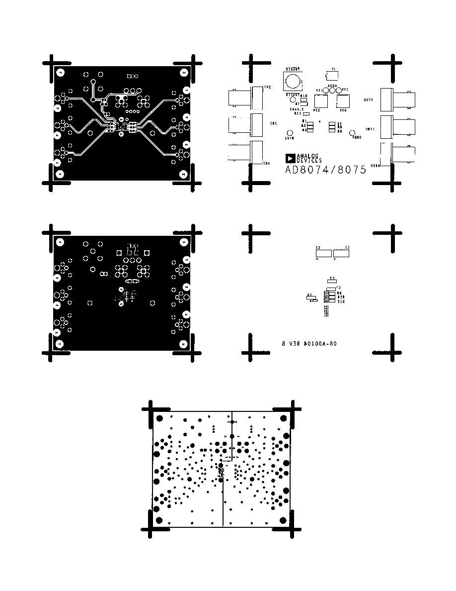
Figure 6. Component Side
Figure 7. Circuit Side
Figure 8. Silkscreen Top
Figure 9. Silkscreen Bottom
Figure 10. Internal 2
REV. A
AD8074/AD8075
15
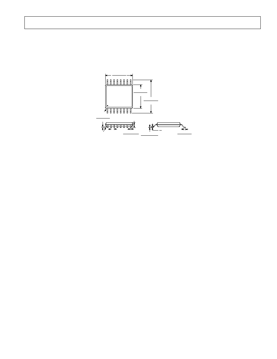
OUTLINE DIMENSIONS
Dimensions shown in inches and (mm).
Controlling Dimension: Metric, shown in parentheses.
16-Lead TSSOP
(RU-16)
16
9
8
1
0.256 (6.50)
0.246 (6.25)
0.177 (4.50)
0.169 (4.30)
PIN 1
0.201 (5.10)
0.193 (4.90)
SEATING
PLANE
0.006 (0.15)
0.002 (0.05)
0.0118 (0.30)
0.0075 (0.19)
0.0256 (0.65)
BSC
0.0433 (1.10)
MAX
0.0079 (0.20)
0.0035 (0.090)
0.028 (0.70)
0.020 (0.50)
8
0

REV. A
16
C02391010/01(A)
PRINTED IN U.S.A.
AD8074/AD8075
16
Revision History
Location
Page
Data Sheet changed from REV. 0 to REV. A.
Addition to equation in SINGLE SUPPLY OPERATION section . . . . . . . . . . . . . . . . . . . . . . . . . . . . . . . . . . . . . . . . . . . . . . . . . . 9
Document Outline
- Specifications
- Pinout
- Package Drawings
- Ordering Guide
- Features
- Applications
- Product Description
- Absolute Maximum Ratings
- Functional Block Diagram
- Circuit Description
- Typical Characteristics
- CAUTION
- MAXIMUM POWER DISSIPATION
- THEORY OF OPERATION
- DIAGRAMS
- Buffer
- Mux
- Evaluation Board Schematic
- Component Side
- Silkscreen Top
- Circuit Side
- Silkscreen Bottom
- Internal 2