 | ÐлекÑÑоннÑй компоненÑ: AD8079 | СкаÑаÑÑ:  PDF PDF  ZIP ZIP |
Äîêóìåíòàöèÿ è îïèñàíèÿ www.docs.chipfind.ru
a
AD8079
FEATURES
Factory Set Gain
AD8079A: Gain = +2.0 (Also +1.0 & 1.0)
AD8079B: Gain = +2.2 (Also +1 & 1.2)
Gain of 2.2 Compensates for System Gain Loss
Minimizes External Components
Tight Control of Gain and Gain Matching (0.1%)
Optimum Dual Pinout
Simplifies PCB Layout
Low Crosstalk of 70 dB @ 5 MHz
Excellent Video Specifications (R
L
= 150 )
Gain Flatness 0.1 dB to 50 MHz
0.01% Differential Gain Error
0.02 Differential Phase Error
Low Power of 50 mW/Amplifier (5 mA)
High Speed and Fast Settling
260 MHz, 3 dB Bandwidth
750 V/ s Slew Rate (2 V Step), 800 V/ s (4 V Step)
40 ns Settling Time to 0.1% (2 V Step)
Low Distortion of 65 dBc THD, f
C
= 5 MHz
High Output Drive of Over 70 mA
Drives Up to 8 Back-Terminated 75 Loads (4 Loads/
Side) While Maintaining Good Differential Gain/
Phase Performance (0.01%/0.17 )
High ESD Tolerance (5 kV)
Available in Small 8-Pin SOIC
APPLICATIONS
Differential A-to-D Driver
Video Line Driver
Differential Line Driver
Professional Cameras
Video Switchers
Special Effects
RF Receivers
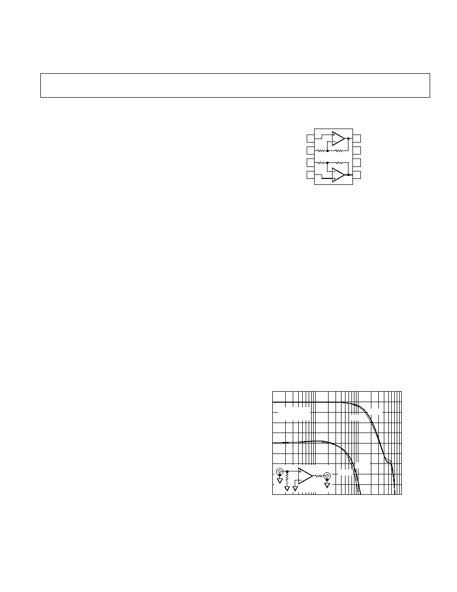
FUNCTIONAL BLOCK DIAGRAM
8-Pin Plastic SOIC
1
2
3
4
5
6
7
8
AD8079
+IN1
GND
GND
+IN2
OUT1
+V
S
V
S
OUT2
Dual 260 MHz
Gain = +2.0 & +2.2 Buffer
REV. A
Information furnished by Analog Devices is believed to be accurate and
reliable. However, no responsibility is assumed by Analog Devices for its
use, nor for any infringements of patents or other rights of third parties
which may result from its use. No license is granted by implication or
otherwise under any patent or patent rights of Analog Devices.
PRODUCT DESCRIPTION
The AD8079 is a dual, low power, high speed buffer designed
to operate on
±
5 V supplies. The AD8079's pinout offers excel-
lent input and output isolation compared to the traditional dual
amplifier pin configuration. With two ac ground pins separating
both the inputs and outputs, the AD8079 achieves very low
crosstalk of less than 70 dB at 5 MHz.
Additionally, the AD8079 contains gain setting resistors factory
set at G = +2.0 (A grade) or Gain = +2.2 (B grade) allowing
circuit configurations with minimal external components. The
B grade gain of +2.2 compensates for gain loss through a system
by providing a single-point trim. Using active laser trimming of
these resistors, the AD8079 guarantees tight control of gain and
channel-channel gain matching. With its performance and con-
figuration, the AD8079 is well suited for driving differential
cables and transformers. Its low distortion and fast settling are
ideal for buffering high speed dual or differential A-to-D con-
verters.
The AD8079 features a unique transimpedance linearization
circuitry. This allows it to drive video loads with excellent differ-
ential gain and phase performance of 0.01% and 0.02
°
on only
50 mW of power per amplifier. It features gain flatness of 0.1 dB
to 50 MHz. This makes the AD8079 ideal for professional video
electronics such as cameras and video switchers.
The AD8079 offers low power of 5 mA/amplifier (V
S
=
±
5 V)
and can run on a single +12 V power supply while delivering
over 70 mA of load current. All of this is offered in a small 8-pin
SOIC package. These features make this amplifier ideal for por-
table and battery powered applications where size and power are
critical.
The outstanding bandwidth of 260 MHz along with 800 V/
µ
s of
slew rate make the AD8079 useful in many general purpose high
speed applications where dual power supplies of
±
3 V to
±
6 V
are required.
The AD8079 is available in the industrial temperature range of
40
°
C to +85
°
C.
FREQUENCY Hz
1M
NORMALIZED FLATNESS dB
1G
10M
100M
0.5
0.1
0
0.1
0.2
0.3
0.4
1
0
9
1
2
3
4
5
6
7
8
NORMALIZED FREQUENCY RESPONSE dB
SIDE 2
SIDE 1
SIDE 2
SIDE 1
R
L
= 100
V
IN
= 50mV rms
50
50
Figure 1. Frequency Response and Flatness
One Technology Way, P.O. Box 9106, Norwood, MA 02062-9106, U.S.A.
Tel: 617/329-4700
World Wide Web Site: http://www.analog.com
Fax: 617/326-8703
© Analog Devices, Inc., 1996

AD8079SPECIFICATIONS
AD8079A/AD8079B
Parameter
Conditions
Min
Typ
Max
Units
DYNAMIC PERFORMANCE
3 dB Small Signal Bandwidth
V
IN
= 50 mV rms
260
MHz
Bandwidth for 0.1 dB Flatness
V
IN
= 50 mV rms
50
MHz
Large Signal Bandwidth
V
IN
= 1 V rms
100
MHz
Slew Rate
V
O
= 2 V Step
750
V/
µ
s
V
O
= 4 V Step
800
V/
µ
s
Settling Time to 0.1%
V
O
= 2 V Step
40
ns
Rise & Fall Time
V
O
= 2 V Step
2.5
ns
NOISE/HARMONIC PERFORMANCE
Total Harmonic Distortion
f
C
= 5 MHz, V
O
= 2 V p-p
65
dBc
Crosstalk, Output to Output
f = 5 MHz
70
dB
Input Voltage Noise
f = 10 kHz
2.0
nV/
Hz
Input Current Noise
f = 10 kHz, +In
2.0
pA/
Hz
Differential Gain Error
NTSC, R
L
= 150
0.01
%
NTSC,
R
L
= 75
0.01
%
Differential Phase Error
NTSC, R
L
= 150
0.02
Degree
R
L
= 75
0.07
Degree
DC PERFORMANCE
Offset Voltage, RTO
10
15
mV
T
MIN
T
MAX
10
20
mV
Offset Drift, RTO
20
µ
V/
°
C
+Input Bias Current
3.0
6.0
±µ
A
T
MIN
T
MAX
10
±µ
A
Gain
No Load
1.998/2.198
2.0/2.2
2.002/2.202
V/V
R
L
= 150
1.995/2.195
2.0/2.2
2.005/2.205
V/V
Gain Matching
Channel-to-Channel, No Load
0.1
%
Channel-to-Channel, R
L
= 150
0.5
%
INPUT CHARACTERISTICS
+Input Resistance
+Input
10
M
+Input Capacitance
+Input
1.5
pF
OUTPUT CHARACTERISTICS
Output Voltage Swing
R
L
= 150
2.7
3.1
±
V
R
L
= 75
2.8
±
V
Output Current
1
70
mA
Short Circuit Current
1
85
110
mA
POWER SUPPLY
Operating Range
±
3.0
±
6.0
V
Quiescent Current/Both Amplifiers
T
MIN
T
MAX
10.0
11.5
mA
Power Supply Rejection Ratio, RTO
+V
S
= +4 V to +6 V, V
S
= 5 V
49
69
dB
V
S
= 4 V to 6 V, +V
S
= +5 V
40
50
dB
+Input Current
T
MIN
T
MAX
0.1
0.5
µ
A/V
NOTES
1
Output current is limited by the maximum power dissipation in the package. See the power derating curves.
Specifications subject to change without notice.
2
REV. A
(@ T
A
= +25 C, V
S
= 5 V, R
L
= 100 , unless otherwise noted)
9
REV. A
AD8079
3
ABSOLUTE MAXIMUM RATINGS
1
Supply Voltage . . . . . . . . . . . . . . . . . . . . . . . . . . . . . . . . 12.6 V
Internal Power Dissipation
2
Small Outline Package (R) . . . . . . . . . . . . . . . . . . 0.9 Watts
Input Voltage . . . . . . . . . . . . . . . . . . . . . . . . . . . . . . . . . . .
±
V
S
Output Short Circuit Duration
. . . . . . . . . . . . . . . . . . . . Observe Power Derating Curves
Storage Temperature Range . . . . . . . . . . . . . 65
°
C to +125
°
C
Operating Temperature Range (A Grade) . . . 40
°
C to +85
°
C
Lead Temperature Range (Soldering 10 sec) . . . . . . . . +300
°
C
NOTES
1
Stresses above those listed under "Absolute Maximum Ratings" may cause
permanent damage to the device. This is a stress rating only and functional
operation of the device at these or any other conditions above those indicated in the
operational section of this specification is not implied. Exposure to absolute
maximum rating conditions for extended periods may affect device reliability.
2
Specification is for device in free air:
8-Pin SOIC Package:
JA
= 160
°
C/Watt
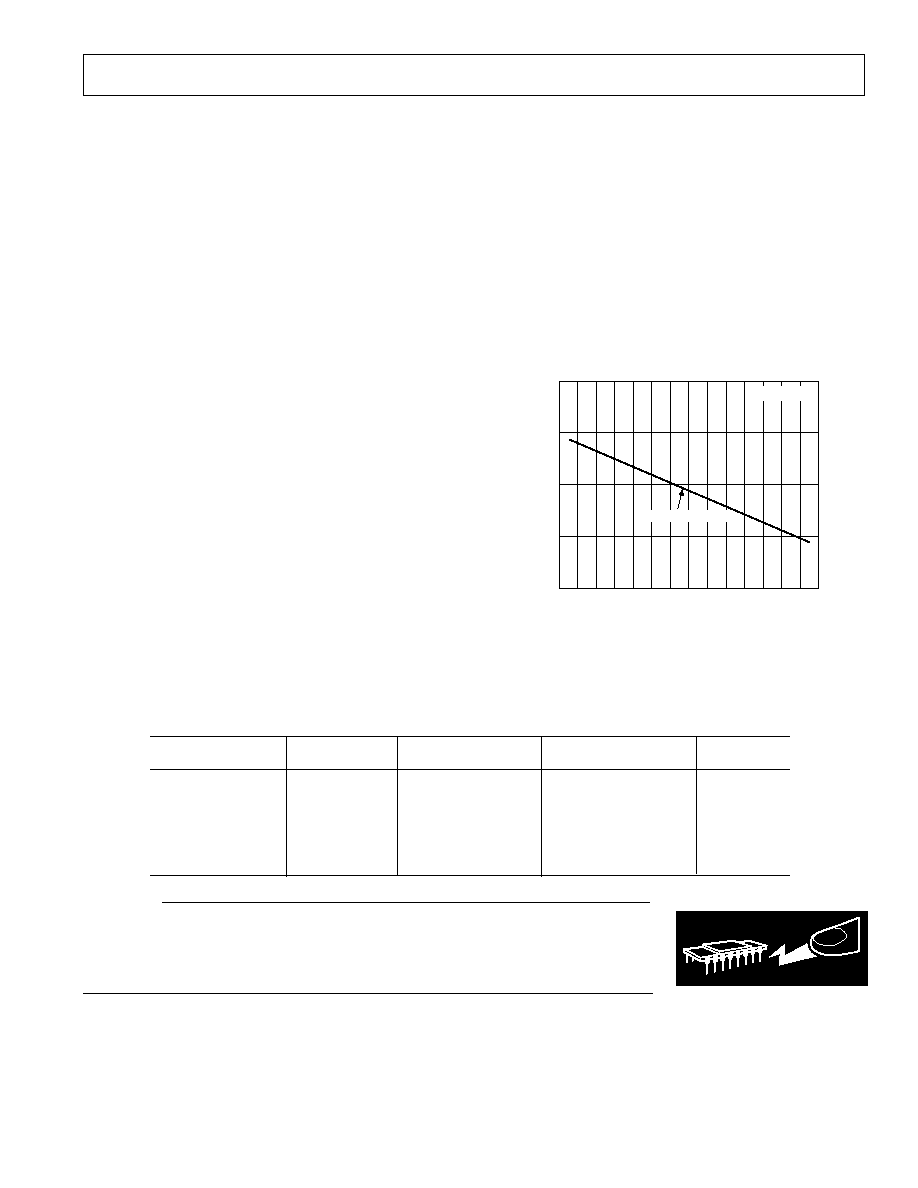
MAXIMUM POWER DISSIPATION
The maximum power that can be safely dissipated by the
AD8079 is limited by the associated rise in junction tempera-
ture. The maximum safe junction temperature for plastic
encapsulated devices is determined by the glass transition tem-
perature of the plastic, approximately +150
°
C. Exceeding this
limit temporarily may cause a shift in parametric performance
due to a change in the stresses exerted on the die by the package.
Exceeding a junction temperature of +175
°
C for an extended
period can result in device failure.
While the AD8079 is internally short circuit protected, this
may not be sufficient to guarantee that the maximum junction
temperature (+150
°
C) is not exceeded under all conditions. To
ensure proper operation, it is necessary to observe the maximum
power derating curves.
MAXIMUM POWER DISSIPATION Watts
AMBIENT TEMPERATURE
°
C
2.0
1.5
0
50
90
40 30 20 10
0
10 20
30 40
50
60
70
1.0
0.5
80
T
J
= +150
°
C
8-PIN SOIC PACKAGE
Figure 2. Plot of Maximum Power Dissipation vs.
Temperature
CAUTION
ESD (electrostatic discharge) sensitive device. Electrostatic charges as high as 4000 V readily
accumulate on the human body and test equipment and can discharge without detection.
Although the AD8079 features proprietary ESD protection circuitry, permanent damage may
occur on devices subjected to high energy electrostatic discharges. Therefore, proper ESD
precautions are recommended to avoid performance degradation or loss of functionality.
WARNING!
ESD SENSITIVE DEVICE
ORDERING GUIDE
Temperature
Package
Package
Model
Gain
Range
Description
Option
AD8079AR
G = +2.0
40
°
C to +85
°
C
8-Pin Plastic SOIC
SO-8
AD8079AR-REEL
G = +2.0
40
°
C to +85
°
C
REEL SOIC
SO-8
AD8079AR-REEL7
G = +2.0
40
°
C to +85
°
C
REEL 7 SOIC
SO-8
AD8079BR
G = +2.2
40
°
C to +85
°
C
8-Pin Plastic SOIC
SO-8
AD8079BR-REEL
G = +2.2
40
°
C to +85
°
C
REEL SOIC
SO-8
AD8079BR-REEL7
G = +2.2
40
°
C to +85
°
C
REEL 7 SOIC
SO-8
AD8079
REV. A
4
FREQUENCY Hz
1M
NORMALIZED FLATNESS dB
1G
10M
100M
0.5
0.1
0
0.1
0.2
0.3
0.4
1
0
9
1
2
3
4
5
6
7
8
NORMALIZED FREQUENCY RESPONSE dB
SIDE 2
SIDE 1
SIDE 2
SIDE 1
R
L
= 100
V
IN
= 50mV rms
50
50
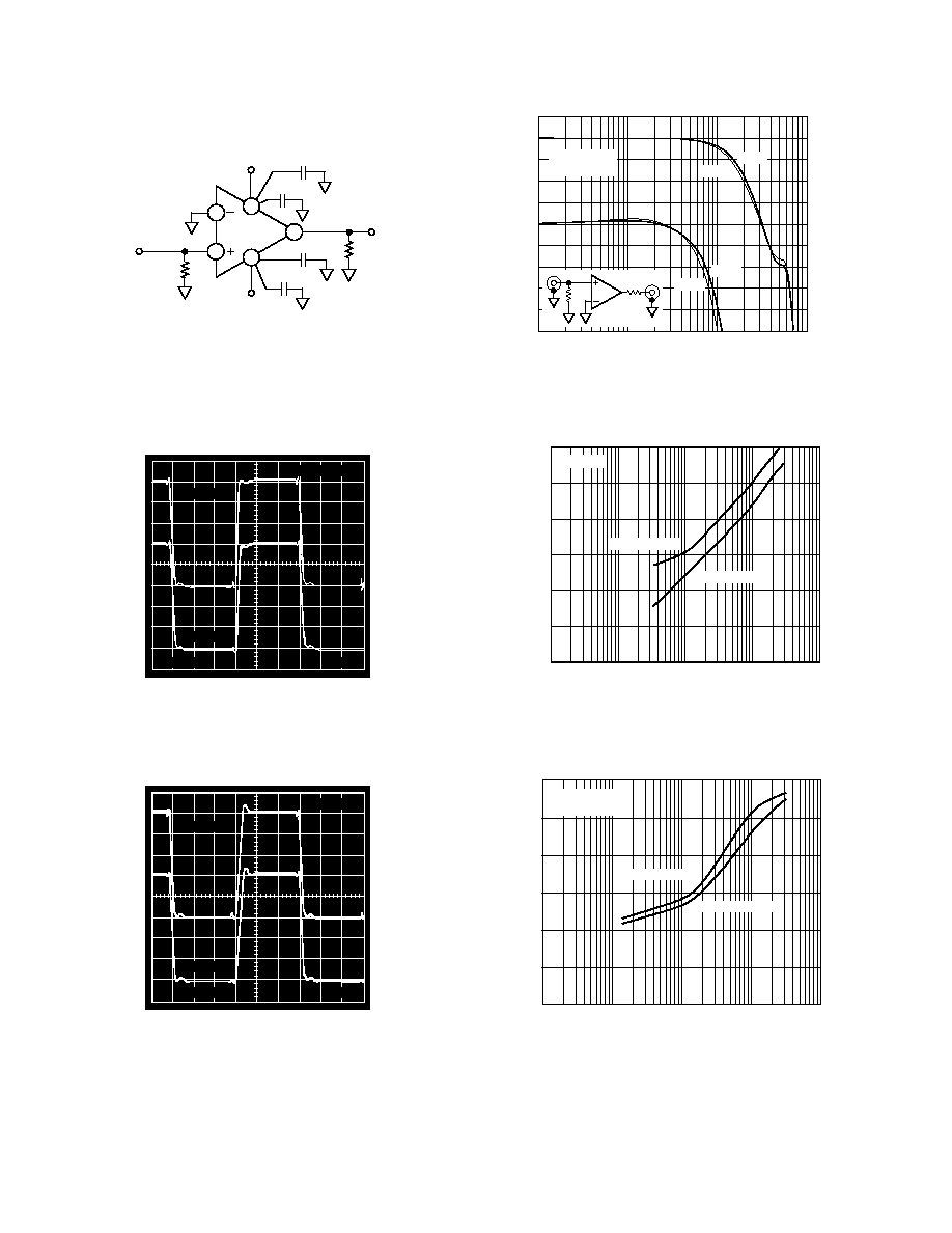
Figure 6. Frequency Response and Flatness
FREQUENCY Hz
50
60
DISTORTION dBc
110
10k
100M
100k
1M
10M
70
80
100
90
2ND HARMONIC
3RD HARMONIC
R
L
= 100
Figure 7. Distortion vs. Frequency, R
L
= 100
60
90
120
100
110
80
70
100k
100M
10M
1M
10k
FREQUENCY Hz
DISTORTION dBc
R
L
= 1k
V
OUT
= 2Vp-p
2ND HARMONIC
3RD HARMONIC
Figure 8. Distortion vs. Frequency, R
L
= 1 k
8
7
6
2
1
AD8079
+5V
10µF
0.1µF
50
V
IN
PULSE
GENERATOR
0.1µF
10µF
5V
R
L
= 100
T
R
/T
F
= 250ps
Figure 3. Test Circuit
20mV
5ns
SIDE 2
SIDE 1
100mV STEP
Figure 4. 100 mV Step Response
200mV
5ns
SIDE 2
SIDE 1
1V STEP
Figure 5. 1 V Step Response
9
REV. A
AD8079
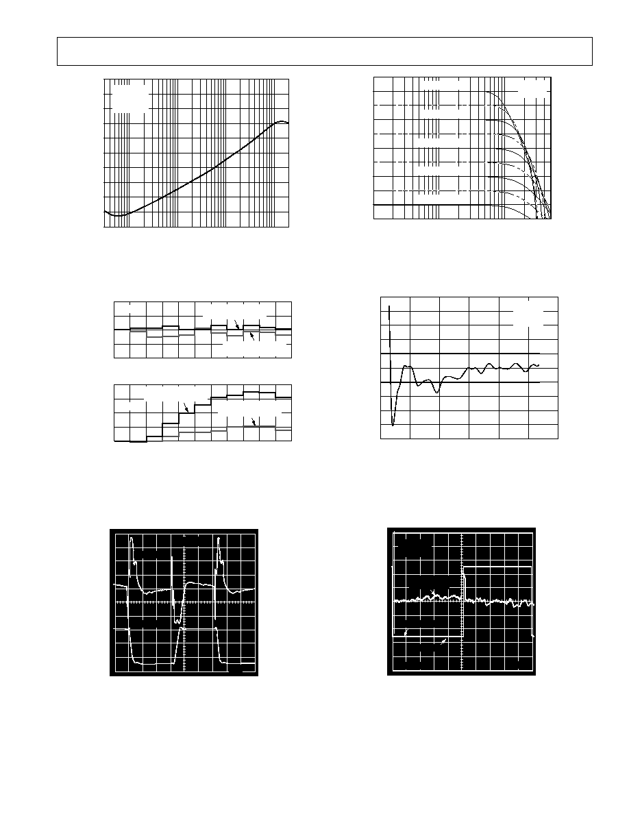
5
CROSSTALK dB
FREQUENCY Hz
100k
200M
0.1M
1M
10M
100M
10
20
110
30
40
50
60
70
80
90
100
V
IN
= 2V p-p
R
L
= 100
V
S
=
±
5V
Figure 9. Crosstalk (Output-to-Output) vs. Frequency
IRE
0.02
0.06
0.00
1
2
DIFF PHASE Degrees
3
4
5
6
7
8
9
10
11
0.01
0.08
0.04
0.02
0.00
0.02
0.01
DIFF GAIN %
2 BACK TERMINATED
LOADS (75
)
1 BACK TERMINATED
LOAD (150
)
2 BACK TERMINATED
LOADS (75
)
1 BACK TERMINATED
LOAD (150
)
NTSC
NTSC
IRE
1
2
3
4
5
6
7
8
9
10
11
Figure 10. Differential Gain and Differential Phase
(per Amplifier)
NOTES: SIDE 1: V
IN
= 0V; 8mV/div RTO
SIDE 2: 1V STEP RTO; 400mV/div
5ns
SIDE 2
SIDE 1
R
L
= 100
Figure 11. Pulse Crosstalk, Worst Case, 1 V Step
FREQUENCY Hz
1M
500M
10M
100M
3
0
27
3
6
9
12
15
18
21
24
3
0
27
3
6
9
12
15
18
21
24
NORMALIZED OUTPUT LEVEL dBV
INPUT LEVEL dBV
V
I N
= 1.0V rms
V
I N
= 0.5V rms
V
I N
= 0.25V rms
V
I N
= 125mV rms
V
I N
= 62.5mV rms
V
S
=
±
5V
R
L
= 100
Figure 12. Large Signal Frequency Response
TIME ns
0.1%/DIV
5
5
0
120
20
40
60
80
100
4
1
2
3
4
3
2
0
1
2V STEP
R
C
= 100
R
L
= 150
Figure 13. Short-Term Settling Time
400mV
2µs
INPUT
OUTPUT
ERROR,
(0.05%/DIV)
2V STEP
R
L
= 100
Figure 14. Long-Term Settling Time
AD8079
REV. A
6
3.4
2.5
125
2.7
2.6
35
55
2.8
2.9
3.0
3.1
3.2
3.3
105
85
65
45
25
5
15
JUNCTION TEMPERATURE
°
C
OUTPUT SWING Volts
+V
OUT
|V
OUT
|
V
S
=
±
5V
R
L
= 150
Figure 15. Output Swing vs. Temperature
JUNCTION TEMPERATURE
°
C
INPUT BIAS CURRENT µA
7
1
55
125
35
15
5
25
45
65
85
105
6
3
2
1
0
5
4
+IN
Figure 16. Input Bias Current vs. Temperature
8
6
0
4
2
6
2
4
125
35
55
105
85
65
45
25
5
15
JUNCTION TEMPERATURE
°
C
INPUT OFFSET VOLTAGE RTO mV
DEVICE #1
DEVICE #2
DEVICE #3
Figure 17. Input Offset Voltage vs. Temperature
11.5
9.0
125
10.5
9.5
35
10.0
55
11.0
105
85
65
45
25
5
15
JUNCTION TEMPERATURE
°
C
TOTAL SUPPLY CURRENT mA
V
S
=
±
5V
Figure 18. Total Supply Current vs. Temperature
120
75
125
85
80
35
55
90
95
100
105
110
115
105
85
65
45
25
5
15
JUNCTION TEMPERATURE
°
C
SHORT CIRCUIT CURRENT mA
|SINK I
SC
|
SOURCE I
SC
70
Figure 19. Short Circuit Current vs. Temperature
FREQUENCY Hz
100
10
1
10
100k
100
NOISE VOLTAGE, RTI nV/ Hz
1k
10k
100
10
1
NOISE CURRENT pA/ Hz
NONINVERTING CURRENT V
S
=
±
5V
VOLTAGE NOISE V
S
=
±
5V
Figure 20. Noise vs. Frequency
9
REV. A
AD8079
7
RESISTANCE
FREQUENCY Hz
10k
1G
100k
1M
10M
100M
100
10
1
0.1
0.01
V
S
=
±
5.0V
POWER = 0dBm
(223.6mV rms)
R
bT
= 50
R
bT
= 0
Figure 21. Output Resistance vs. Frequency
44.0
66.5
125
61.5
64.0
35
55
59.0
56.5
54.0
51.5
49.0
46.5
105
85
65
45
25
5
15
JUNCTION TEMPERATURE
°
C
PSRR dB
69.0
PSRR
+PSRR
2V SPAN
CURVES ARE FOR WORST
CASE CONDITION WHERE
ONE SUPPLY IS VARIED
WHILE THE OTHER IS
HELD CONSTANT.
Figure 22. PSRR vs. Temperature
PSRR dB
FREQUENCY Hz
0
4
84
30k
500M
100k
1M
10M
100M
14
24
64
34
44
54
74
V
IN
= 200mV
PSRR
+PSRR
Figure 23. PSRR vs. Frequency
THEORY OF OPERATION
The AD8079, a dual current feedback amplifier, is internally
configured for a gain of either +2 (AD8079A) or +2.2
(AD8079B). The internal gain-setting resistors effectively elimi-
nate any parasitic capacitance associated with the inverting in-
put pin, accounting for the AD8079's excellent gain flatness
response. The carefully chosen pinout greatly reduces the cross-
talk between each amplifier. Up to four back-terminated 75
video loads can be driven by each amplifier, with a typical dif-
ferential gain and phase performance of 0.01%/0.17
°
, respec-
tively. The AD8079B, with a gain of +2.2, can be employed as a
single gain-trimming element in a video signal chain. Finally,
the AD8079A/B used in conjunction with our AD8116 cross-
point matrix, provides a complete turn-key solution to video
distribution.
Printed Circuit Board Layout Considerations
As to be expected for a wideband amplifier, PC board parasitics
can affect the overall closed-loop performance. If a ground
plane is to be used on the same side of the board as the signal
traces, a space (5 mm min) should be left around the signal lines
to minimize coupling. Line lengths on the order of less than
5 mm are recommended. If long runs of coaxial cable are being
driven, dispersion and loss must be considered.
Power Supply Bypassing
Adequate power supply bypassing can be critical when optimiz-
ing the performance of a high frequency circuit. Inductance in
the power supply leads can form resonant circuits that produce
peaking in the amplifier's response. In addition, if large current
transients must be delivered to the load, then bypass capacitors
(typically greater than 1
µ
F) will be required to provide the best
settling time and lowest distortion. A parallel combination of
4.7
µ
F and 0.1
µ
F is recommended. Some brands of electrolytic
capacitors will require a small series damping resistor
4.7
for optimum results.
DC Errors and Noise
There are three major noise and offset terms to consider in a
current feedback amplifier. For offset errors refer to the equa-
tion below. For noise error the terms are root-sum-squared to
give a net output error. In the circuit below (Figure 24) they are
input offset (V
IO
) which appears at the output multiplied by the
noise gain of the circuit (1 + R
F
/R
I
), noninverting input current
(I
BN
×
R
N
) also multiplied by the noise gain, and the inverting
input current, which when divided between R
F
and R
I
and sub-
sequently multiplied by the noise gain always appears at the out-
put as I
BN
×
R
F
. The input voltage noise of the AD8079 is a low
2 nV/
Hz
. At low gains though the inverting input current noise
times R
F
is the dominant noise source. Careful layout and de-
vice matching contribute to better offset and drift specifications
for the AD8079 compared to many other current feedback am-
plifiers. The typical performance curves in conjunction with the
equations below can be used to predict the performance of the
AD8079 in any application.
V
OUT
=
V
IO
×
1
+
R
F
R
I
±
I
BN
×
R
N
×
1
+
R
F
R
I
±
I
BI
×
R
F
where:
R
F
= R
I
= 750
for AD8079A
R
F
= 750
, R
I
= 625
for AD8079B
AD8079
REV. A
8
8
7
6
2
1
5
4
3
V
OUT
#1
75
75
CABLE
75
V
OUT
#2
75
75
CABLE
75
75
75
CABLE
V
I N
+V
S
V
S
V
OUT
#3
75
75
CABLE
75
V
OUT
#4
75
75
CABLE
75
1/2
AD8079
1/2
AD8079
4.7µF
4.7µF
0.1µF
0.1µF
Figure 26. Video Line Driver
Single-Ended to Differential Driver Using an AD8079
The two halves of an AD8079 can be configured to create a
single-ended to differential high speed driver with a 3 dB band-
width in excess of 110 MHz as shown in Figure 27. Although
the individual op amps are each current feedback with internal
feedback resistors, the overall architecture yields a circuit with
attributes normally associated with voltage feedback amplifiers,
while offering the speed advantages inherent in current feedback
amplifiers. In addition, the gain of the circuit can be changed by
varying a single resistor, R
F
, which is often not possible in a dual
op amp differential driver.
50
OUTPUT #1
50
OUTPUT #2
R
G
750
R
F
750
1/2
AD8079
1/2
AD8079
OP AMP #1
OP AMP #2
V
IN
C
C
= 1.5pF
Figure 27. Differential Line Driver
V
OUT
R
F
( INTERNAL)
R
N
I
B I
I
B N
R
I
( INTERNAL)
R
SERIES
C
L
Figure 24. Output Offset Voltage
Driving Capacitive Loads
The AD8079 was designed primarily to drive nonreactive loads.
If driving loads with a capacitive component is desired, best
frequency response is obtained by the addition of a small series
output resistance (R
SERIES
). The graph in Figure 25 shows the
optimum value for R
SERIES
vs. capacitive load. It is worth noting
that the frequency response of the circuit when driving large
capacitive loads will be dominated by the passive roll-off of
R
SERIES
and C
L
.
C
L
pF
40
30
0
0
25
5
R
SERIES
10
15
20
20
10
Figure 25. Recommended R
SERIES
vs. Capacitive Load
Operation as a Video Line Driver
The AD8079 has been designed to offer outstanding perfor-
mance as a video line driver. The important specifications of
differential gain (0.01%) and differential phase (0.02
°
) meet the
most exacting HDTV demands for driving one video load with
each amplifier. The AD8079 also drives four back terminated
loads (two each), as shown in Figure 26, with equally impressive
performance (0.01%, 0.07
°
). Another important consideration is
isolation between loads in a multiple load application. The
AD8079 has more than 40 dB of isolation at 5 MHz when driv-
ing two 75
back terminated loads.
9
REV. A
AD8079
9
The current feedback nature of the op amps, in addition to
enabling the wide bandwidth, provides an output drive of more
than 3 V p-p into a 20
load for each output at 20 MHz. On
the other hand, the voltage feedback nature provides symmetri-
cal high impedance inputs and allows the use of reactive compo-
nents in the feedback network.
The circuit consists of the two op amps each configured as a
unity gain follower by the 750
feedback resistors between
each op amp's output and inverting input. The output of each
op amp has a 750
resistor to the inverting input of the other
op amp. Thus, each output drives the other op amp through a
unity gain inverter configuration. By connecting the two ampli-
fiers as cross-coupled inverters, their outputs are free to be equal
and opposite, assuring zero-output common-mode voltage.
With this circuit configuration, the common-mode signal of the
outputs is reduced. If one output moves slightly higher, the
negative input to the other op amp drives its output to go
slightly lower and thus preserves the symmetry of the comple-
mentary outputs which reduces the common-mode signal.
The resulting architecture offers several advantages. First, the
gain can be changed by changing a single resistor. Changing
either R
F
or R
G
will change the gain as in an inverting op amp
circuit. For most types of differential circuits, more than one
resistor must be changed to change gain and still maintain good
CMR.
Reactive elements can be used in the feedback network. This is
in contrast to current feedback amplifiers that restrict the use of
reactive elements in the feedback. The circuit described requires
about 1.3 pF of capacitance in shunt across R
F
in order to opti-
mize peaking and realize a 3 dB bandwidth of more than
110 MHz.
The peaking exhibited by the circuit is very sensitive to the
value of this capacitor. Parasitics in the board layout on the or-
der of tenths of picofarads will influence the frequency response
and the value required for the feedback capacitor, so a good lay-
out is essential.
The shunt capacitor type selection is also critical. Good micro-
wave type chip capacitors with high Q were found to yield best
performance.
FREQUENCY Hz
0.1M
1G
1M
10M
100M
C
C
= 1.3pF
V
IN
= 10dBm
6
4
2
0
2
4
6
8
10
12
14
OUTPUT dB
OUT+
OUT
Figure 28. Differential Driver Frequency Response
Layout Considerations
The specified high speed performance of the AD8079 requires
careful attention to board layout and component selection.
Proper RF design techniques and low parasitic component se-
lection are mandatory.
The PCB should have a ground plane covering all unused por-
tions of the component side of the board to provide a low im-
pedance ground path. The ground plane should be removed
from the area near the input pins to reduce stray capacitance.
Chip capacitors should be used for supply bypassing (see Figure
29). One end should be connected to the ground plane and the
other within 1/8 in. of each power pin. An additional large
(4.7
µ
F10
µ
F) tantalum electrolytic capacitor should be con-
nected in parallel, but not necessarily so close, to supply current
for fast, large-signal changes at the output.
Stripline design techniques should be used for long signal traces
(greater than about 1 in.). These should be designed with a
characteristic impedance of 50
or 75
and be properly termi-
nated at each end.
AD8079
REV. A
10
+V
S
V
S
R
T
IN
50
OUT
+V
S
V
S
C1
0.1µF
C3
10µF
C2
0.1µF
C4
10µF
+V
S
V
S
R
T
50
OUT
IN
*
SEE TABLE I
Supply Bypassing
Inverting Configuration
Noninverting Configuration (G = +2)
+V
S
V
S
R
T
OUT
IN
TIE INPUT PINS
TOGETHER
TO MINIMIZE
PEAKING
Noninverting Configuration (G = +1)
R
T
OUT
IN
AD8079B
TRIM
200
Optional Gain Trim (G = +2
+
2.2)
Figure 29. Inverting and Noninverting Configurations
Table I. Recommended Component Values
Component
1
+1
+2/+2.2
R
T
(Nominal) (
)
53.6
49.9
49.9
Small Signal BW (MHz)
220
750
260
0.1 dB Flatness (MHz)
50
100
50
Figure 30. Board Layout (Silkscreen)
Figure 31. Board Layout (Component Layer)
Figure 32. Board Layout (Solder Side; Looking Through
the Board)
9
REV. A
AD8079
11
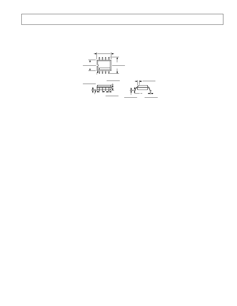
OUTLINE DIMENSIONS
Dimensions shown in inches and (mm).
8-Lead SOIC (SO-8)
0.1968 (5.00)
0.1890 (4.80)
8
5
4
1
0.2440 (6.20)
0.2284 (5.80)
PIN 1
0.1574 (4.00)
0.1497 (3.80)
0.0688 (1.75)
0.0532 (1.35)
SEATING
PLANE
0.0098 (0.25)
0.0040 (0.10)
0.0192 (0.49)
0.0138 (0.35)
0.0500
(1.27)
BSC
0.0098 (0.25)
0.0075 (0.19)
0.0500 (1.27)
0.0160 (0.41)
8
°
0
°
0.0196 (0.50)
0.0099 (0.25)
x 45
°

C2185axx11/96
PRINTED IN U.S.A.
12