 | ÐлекÑÑоннÑй компоненÑ: AD8170AR | СкаÑаÑÑ:  PDF PDF  ZIP ZIP |
Äîêóìåíòàöèÿ è îïèñàíèÿ www.docs.chipfind.ru
REV. 0
Information furnished by Analog Devices is believed to be accurate and
reliable. However, no responsibility is assumed by Analog Devices for its
use, nor for any infringements of patents or other rights of third parties
which may result from its use. No license is granted by implication or
otherwise under any patent or patent rights of Analog Devices.
a
AD8170/AD8174
One Technology Way, P.O. Box 9106, Norwood, MA 02062-9106, U.S.A.
Tel: 617/329-4700
World Wide Web Site: http://www.analog.com
Fax: 617/326-8703
© Analog Devices, Inc., 1996
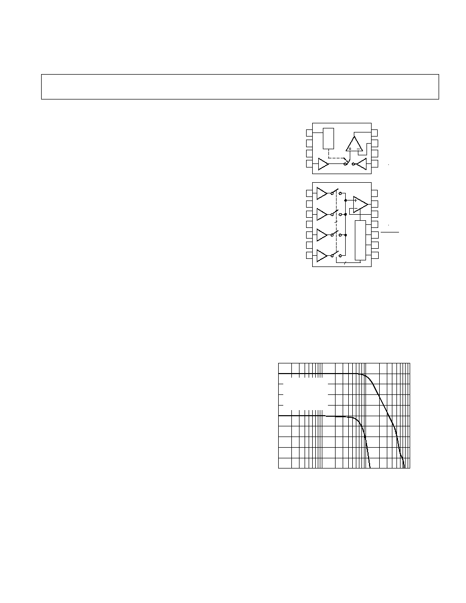
FUNCTIONAL BLOCK DIAGRAM
1
2
3
4
8
7
6
5
AD8170
+1
+1
LOGIC
V
OUT
V
IN
+V
S
IN1
SELECT
GND
V
S
IN0
10
9
8
+1
AD8174
+1
+1
+1
2
2
14
13
12
11
1
2
3
4
5
6
7
LOGIC
+V
S
V
OUT
V
IN
SD
ENABLE
A1
A0
IN0
GND
IN1
GND
IN2
V
S
IN3
250 MHz, 10 ns Switching
Multiplexers w/Amplifier
FEATURES
Fully Buffered Inputs and Outputs
Fast Channel Switching: 10 ns
Internal Current Feedback Output Amplifier
High Output Drive: 50 mA
Flexible Gain Setting via External Resistor(s)
High Speed
250 MHz Bandwidth, G = +2
1000 V/ s Slew Rate
Fast Settling Time of 15 ns to 0.1%
Low Power: < 10 mA
Excellent Video Specifications (R
L
= 150 ,
G = +2)
Gain Flatness of 0.1 dB Beyond 80 MHz
0.02% Differential Gain Error
0.05 Differential Phase Error
Low Crosstalk of 78 dB @ 5 MHz
High Disable Isolation of 88 dB @ 5 MHz
High Shutdown Isolation of 92 dB @ 5 MHz
Low Cost
Fast Output Disable Feature for Connecting Multiple
Devices (AD8174 Only)
Shutdown Feature Reduces Power to 1.5 mA (AD8174 Only)
APPLICATIONS
Pixel Switching for "Picture-In-Picture"
LCD and Plasma Displays
Video Routers
PRODUCT DESCRIPTION
The AD8170(2:1) and AD8174(4:1) are very high speed
buffered multiplexers. These multiplexers offer an internal
current feedback output amplifier whose gain can be pro-
grammed via external resistors and is capable of delivering 50
mA of output current. They offer 3 dB signal bandwidth of
250 MHz and slew rate of greater than 1000 V/
µ
s. Additionally,
the AD8170 and AD8174 have excellent video specifications
with low differential gain and differential phase error of 0.02%
and 0.05
°
and 0.1 dB flatness out to 80 MHz. With a low 78
dB of crosstalk and better than 88 dB isolation, these devices are
useful in many high speed applications. These are low power
devices consuming only 9.7 mA from a
±
5 V supply.
The AD8174 offers a high speed disable feature allowing the
output to be put into a high impedance state for cascading
stages so that the off channels do not load the output bus.
Additionally, the AD8174 can be shut down (SD) when not in
use to minimize power consumption (I
S
= 1.5 mA). These
products will be offered in 8-lead and 14-lead PDIP and SOIC
packages.
NORMALIZED OUTPUT dB
V
IN
= 50mV rms
G = +2
R
F
= 499
(AD8170R)
R
F
= 549
(AD8174R)
R
L
= 100
FREQUENCY Hz
0.5
NORMALIZED FLATNESS dB
0.1
0.2
0.3
0.4
0.1
0
0
9
5
6
7
8
3
4
1
2
1M
10M
100M
1G
Figure 1. Small Signal Frequency Response
2
REV. 0
AD8170/AD8174SPECIFICATIONS
(@ T
A
= +25 C, V
S
= 5 V, R
L
= 150
, G = +2, R
F
= 499
(AD8170R), R
F
= 549
(AD8174R) unless otherwise noted)
AD8170A/AD8174A
Parameter
Conditions
Min
Typ
Max
Units
SWITCHING CHARACTERISTICS
Switching Time
1
Channel-to-Channel
50% Logic to 10% Output Settling
IN0, IN2 = +0.5 V; IN1, IN3 = 0.5 V
7.5
ns
50% Logic to 90% Output Settling
IN0, IN2 = +0.5 V; IN1, IN3 = 0.5 V
9.1
ns
50% Logic to 99.9% Output Settling
IN0, IN2 = +0.5 V; IN1, IN3 = 0.5 V
25
ns
ENABLE
to Channel ON Time
2
(AD8174R)
50% Logic to 90% Output Settling
IN0, IN2 = +0.5 V; IN1, IN3 = 0.5 V
17
ns
ENABLE
to Channel OFF Time
2
(AD8174R)
50% Logic to 90% Output Settling
IN0, IN2 = +0.5 V; IN1, IN3 = 0.5 V
120
ns
Shutdown to Channel ON Time
3
(AD8174R)
50% Logic to 90% Output Settling
IN0, IN2 = +0.5 V; IN1, IN3 = 0.5 V
20
ns
Shutdown to Channel OFF Time
3
(AD8174R)
50% Logic to 90% Output Settling
IN0, IN2 = +0.5 V; IN1, IN3 = 0.5 V
115
ns
Channel Switching Transient (Glitch)
4
All Inputs Grounded
138 /104
mV p-p
DIGITAL INPUTS
Logic "1" Voltage
SELECT, A0, A1, ENABLE, SD Inputs, T
MIN
T
MAX
2.0
V
Logic "0" Voltage
SELECT, A0, A1, ENABLE, SD Inputs, T
MIN
T
MAX
0.8
V
Logic "1" Input Current
SELECT, A0, A1 Inputs, T
MIN
T
MAX
50
300
nA
ENABLE
, SD Inputs, T
MIN
T
MAX
1
5
µ
A
Logic "0" Input Current
SELECT, A0, A1 Inputs, T
MIN
T
MAX
3
5
µ
A
ENABLE
, SD Inputs, T
MIN
T
MAX
30
300
nA
DYNAMIC PERFORMANCE
3 dB Bandwidth (Small Signal)
5
V
O
= 50 mV rms, R
L
= 100
250
MHz
3 dB Bandwidth (Large Signal)
5
V
O
= 1 V rms, R
L
= 100
100
MHz
0.1 dB Bandwidth
5
V
O
= 50 mV rms, R
F
= 499
(AD8170R), R
L
= 100
V
O
= 50 mV rms, R
F
= 549
(AD8174R), R
L
= 100
85
MHz
Rise and Fall Time (10% to 90%)
2 V Step
1.6
ns
Slew Rate
2 V Step
1000
V/
µ
s
Settling Time to 0.1%
2 V Step
15
ns
DISTORTION/NOISE PERFORMANCE
Differential Gain
= 3.58 MHz
0.02
%
Differential Phase
= 3.58 MHz
0.05
Degrees
All Hostile Crosstalk
6
AD8170R
= 5 MHz, R
L
= 100
80
dB
= 30 MHz, R
L
= 100
65
dB
All Hostile Crosstalk
6
AD8174R
= 5 MHz, R
L
= 100
78
dB
= 30 MHz, R
L
= 100
63
dB
Disable Isolation
7
AD8174R
= 5 MHz, R
L
= 100
88
dB
= 30 MHz, R
L
= 100
72
dB
Shutdown Isolation
8
AD8174R
= 5 MHz, R
L
= 100
92
dB
= 30 MHz, R
L
= 100
77
dB
Input Voltage Noise
= 10 kHz to 30 MHz
10
nV/
Hz
+Input Current Noise
= 10 kHz to 30 MHz
1.6
pA/
Hz
Input Current Noise
= 10 kHz to 30 MHz
8.5
pA/
Hz
Total Harmonic Distortion
C
= 10 MHz, V
O
= 2 V p-p, R
L
= 150
60
dBc
C
= 10 MHz, V
O
= 2 V p-p, R
L
= 1 k
72
dBc
DC/TRANSFER CHARACTERISTICS
Transresistance
400
600
k
Open-Loop Voltage Gain
2000
6000
V/V
Gain Accuracy
9
G = +1, R
F
= 1 k
0.4
%
Gain Matching
Channel-to-Channel
0.05
%
Input Offset Voltage
5
9
mV
T
MIN
to T
MAX
12
mV
Input Offset Voltage Matching
Channel-to-Channel
1.5
5
mV
Input Offset Voltage Drift
11
µ
V/
°
C
Input Bias Current
(+) Switch Input
7
15
µ
A
T
MIN
to T
MAX
15
µ
A
() Buffer Input
3
10
µ
A
T
MIN
to T
MAX
14
µ
A
Input Bias Current Drift
(+) Switch and () Buffer Input
20
nA/
°
C

3
REV. 0
AD8170/AD8174
AD8170A/AD8174A
Parameter
Conditions
Min
Typ
Max
Units
INPUT CHARACTERISTICS
Input Resistance
(+) Switch Input
1.7
M
() Buffer Input
100
Input Capacitance
Channel Enabled (R Package)
1.1
pF
Channel Disabled (R Package)
1.1
pF
Input Voltage Range
±
3.3
V
Input Common-Mode Rejection Ratio
+CMRR,
V
CM
= 1 V
51
56
dB
CMRR,
V
CM
= 1 V
50
52
dB
OUTPUT CHARACTERISTICS
Output Voltage Swing
R
L
= 1 k
, T
MIN
T
MAX
±
4.0
±
4.26
V
R
L
= 150
, T
MIN
T
MAX
±
3.5
±
4.0
V
Output Current
R
L
= 10
50
mA
Short Circuit Current
180
mA
Output Resistance
Enabled
10
m
Disabled (AD8174)
10
M
Output Capacitance
Disabled (AD8174)
7.5
pF
POWER SUPPLY
Operating Range
±
4
±
6
V
Power Supply Rejection Ratio
+PSRR
+V
S
= +4.5 V to +5.5 V, V
S
= 5 V
58
66
dB
T
MIN
T
MAX
55
dB
Power Supply Rejection Ratio
PSRR
V
S
= 4.5 V to 5.5 V, +V
S
= +5 V
52
58
dB
T
MIN
T
MAX
50
dB
Quiescent Current
All Channels "ON", T
MIN
T
MAX
8.7/9.7
11/13
mA
AD8174 Disabled, T
MIN
T
MAX
4.1
5
mA
AD8174 Shutdown, T
MIN
T
MAX
1.5
2.5
mA
OPERATING TEMPERATURE RANGE
40
+85
°
C
NOTES
1
Shutdown (SD) and ENABLE pins are grounded (AD8174). IN0 (or IN2) = +0.5 V dc, IN1 (or IN3) = 0.5 V dc. SELECT (A0 or A1 for AD8174) input is
driven with 0 V to +5 V pulse. Measure transition time from 50% of SELECT (A0 or A1) input value (+2.5 V) and 10% (or 90%) of the total output voltage transi-
tion from IN0 (or IN2) channel voltage (+0.5 V) to IN1 (or IN3 = 0.5 V) or vice versa.
2
AD8174 only. Shutdown (SD) pin is grounded. ENABLE pin is driven with 0 V to +5 V pulse (5 ns rise and fall times). State of A0 and A1 logic inputs determines
which channel is activated (i.e., if A0 = Logic 0 and A1 = Logic 1, then IN2 input is selected). Set IN0 (or IN2) = +0.5 V dc, IN1 (or IN3) = 0.5 V dc, and mea-
sure transition time from 50% of ENABLE pulse (+2.5 V) to 90% of the total output voltage change. In Figure 5,
t
OFF
is the disable time,
t
ON
is the enable time.
3
AD8174 only. ENABLE pin is grounded. Shutdown (SD) pin is driven with 0 V to +5 V pulse (5 ns rise and fall times). State of A0 and A1 logic inputs determines
which channel is activated (i.e., if A0 = Logic 1 and A1 = Logic O, then IN1 input is selected). Set IN0 (or IN2) = +0.5 V dc, IN1 (or IN3) = 0.5 V dc, and mea-
sure transition time from 50% of SD pulse (+2.5 V) to 90% of the total output voltage change. In Fig ure 6,
t
OFF
is the shutdown assert time,
t
ON
is the shutdown
release time.
4
All inputs are grounded. SELECT (A0 or A1 for AD8174) input is driven with 0 V to +5 V pulse. The outputs are monitored. Speeding the edges of the SELECT
(A0 or A1) pulse increases the glitch magnitude due to coupling via the ground plane.
5
Bandwidth of the multiplexer is dependent upon the resistor feedback network. Refer to Table III for recommended feedback component values, which give the best
compromise between a wide and a flat frequency response.
6
Select input(s) that is (are) not being driven (i.e., if SELECT is Logic 1, activated input is IN1; in AD8174, if A0 = Logic 0, A1 = Logic 1, activated input is IN2).
Drive all other inputs with V
IN
= 0.707 V rms, and monitor output at f = 5 MHz and 30 MHz;
R
L
= 100
(see Figure 13).
7
AD8174 only. Shutdown (SD) pin is grounded. Mux is disabled, (i.e., ENABLE = Logic 1) and all inputs are driven simultaneously with V
IN
= 0.354 V rms. Out-
put is monitored at f = 5 MHz and 30 MHz; R
L
= 100
. In this mode, the output impedance of the disabled mux is very high (typ 10 M
), and the signal couples
across the package; the load impedance and the feedback network determine the crosstalk. For instance, in a closed-loop gain of +1, r
OUT
10 M
, in a gain of +2
(R
F
= R
G
= 549
), r
OUT
= 1.1 k
(see Figure 14).
8
AD8174 only. ENABLE pin is grounded. Mux is shutdown (i.e., SD = Logic 1), and all inputs are driven simultaneously with V
IN
= 0.354 V rms. Output is moni-
tored at f = 5 MHz and 30 MHz;
R
L
= 100
. (see Figure 14). The mux output impedance in shutdown mode is the same as the disabled mux output impedance.
9
For Gain Accuracy expression, refer to Equation 4.
Specifications subject to change without notice.
Table I. AD8170 Truth Table
SELECT
V
OUT
0
IN0
1
IN1
Table II. AD8174 Truth Table
A0
A1
ENABLE
SD
V
OUT
0
0
0
0
IN0
1
0
0
0
IN1
0
1
0
0
IN2
1
1
0
0
IN3
X
X
1
0
HIGH Z, I
S
= 4.1 mA
X
X
X
1
HIGH Z, I
S
= 1.5 mA

AD8170/AD8174
4
REV. 0
WARNING!
ESD SENSITIVE DEVICE
CAUTION
ESD (electrostatic discharge) sensitive device. Electrostatic charges as high as 4000 V readily
accumulate on the human body and test equipment and can discharge without detection.
Although the AD8170/AD8174 feature proprietary ESD protection circuitry, permanent damage
may occur on devices subjected to high energy electrostatic discharges. Therefore, proper ESD
precautions are recommended to avoid performance degradation or loss of functionality.
ABSOLUTE MAXIMUM RATINGS
1
Supply Voltage . . . . . . . . . . . . . . . . . . . . . . . . . . . . . . . . 12.6 V
Internal Power Dissipation
2
AD8170 8-Lead Plastic (N) . . . . . . . . . . . . . . . . . 1.3 Watts
AD8170 8-Lead Small Outline (R) . . . . . . . . . . . 0.9 Watts
AD8174 14-Lead Plastic (N) . . . . . . . . . . . . . . . . 1.6 Watts
AD8174 14-Lead Small Outline (R) . . . . . . . . . . 1.0 Watts
Input Voltage (Common Mode) . . . . . . . . . . . . . . . . . . . .
±
V
S
Output Short Circuit Duration . . Observe Power Derating Curves
Storage Temperature Range
N & R Packages . . . . . . . . . . . . . . . . . . . . 65
°
C to +125
°
C
Lead Temperature Range (Soldering 10 sec) . . . . . . . . +300
°
C
NOTES
1
Stresses above those listed under "Absolute Maximum Ratings" may cause
permanent damage to the device. This is a stress rating only and functional
operation of the device at these or any other conditions above those indicated in
the operational section of this specification is not implied. Exposure to absolute
maximum rating conditions for extended periods may affect device reliability.
2
Specification is for device in free air: 8-Pin Plastic Package:
JA
= 90
°
C/Watt;
8-Pin SOIC Package:
JA
= 160
°
C/Watt; 14-Pin Plastic Package:
JA
= 90
°
C/Watt
14-Pin SOIC Package:
JA
= 120
°
C/Watt, where P
D
= (T
J
T
A
)/
JA
.
ORDERING GUIDE
Temperature
Package
Package
Model
Range
Description
Option
AD8170AN
40
°
C to +85
°
C
8-Pin Plastic DIP
N-8
AD8170AR
40
°
C to +85
°
C
8-Pin SOIC
SO-8
AD8170AR-REEL 40
°
C to +85
°
C
Reel 8-Pin SOIC
SO-8
AD8174AN
40
°
C to +85
°
C
14-Pin Plastic DIP
N-14
AD8174AR
40
°
C to +85
°
C
14-Pin Narrow SOIC R-14
AD8174AR-REEL 40
°
C to +85
°
C
Reel 14-Pin SOIC
R-14
AD8170-EB
Evaluation Board For AD8170R
AD8174-EB
Evaluation Board For AD8174R
MAXIMUM POWER DISSIPATION
The maximum power that can be safely dissipated by the
AD8170 and AD8174 is limited by the associated rise in
junction temperature. The maximum safe junction temperature
for plastic encapsulated devices is determined by the glass
transition temperature of the plastic, approximately +150
°
C.
Exceeding this limit temporarily may cause a shift in parametric
performance due to a change in the stresses exerted on the die
by the package. Exceeding a junction temperature of +175
°
C
for an extended period can result in device failure.
While the AD8170 and AD8174 are internally short circuit
protected, this may not be sufficient to guarantee that the maxi-
mum junction temperature (+150
°
C) is not exceeded under all
conditions. To ensure proper operation, it is necessary to observe
the maximum power derating curves shown in Figures 2 and 3.
MAXIMUM POWER DISSIPATION Watts
AMBIENT TEMPERATURE
°
C
2.0
1.5
0
50
90
40 30 20 10
0
10
20
30
50
60
70
80
40
1.0
0.5
8-PIN MINI-DIP PACKAGE
8-PIN SOIC PACKAGE
T
J
= +150
°
C
Figure 2. AD8170 Maximum Power Dissipation vs.
Temperature
AMBIENT TEMPERATURE
°
C
2.5
2.0
0.5
50
90
40
MAXIMUM POWER DISSIPATION Watts
30 20 10
0
10 20
30
40 50
60
80
1.5
1.0
70
14-PIN SOIC
14-PIN DIP PACKAGE
T
J
= +150
°
C
Figure 3. AD8174 Maximum Power Dissipation vs.
Temperature
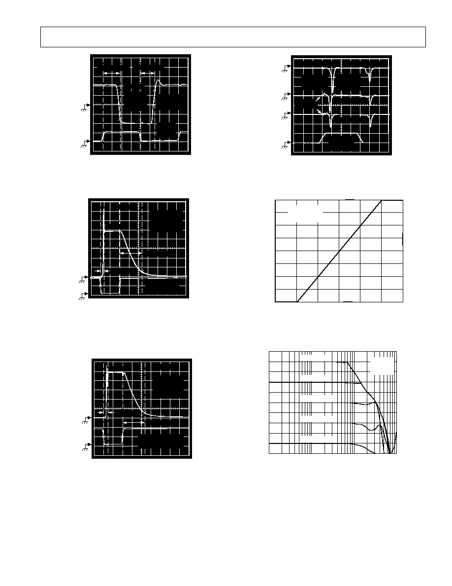
5ns/DIV
500mV/DIV
DUT
OUT
t
FALL
= 9.1ns
t
RISE
= 7.5ns
OUTPUT
IN0, IN2 =
+0.5V
IN1, IN3 =
+0.5V
SELECT
PULSE
0 TO +5V
G = +2
R
F
= R
G
= 499
R
L
= 100
Figure 4. Channel Switching Characteristics
50ns/DIV
200mV/DIV
ENABLE
PULSE
0 TO +5V
(5nsec EDGES)
INØ = +0.5VDC
G = +2
R
F
= 549
R
L
= 100
t
OFF
= 120ns
t
ON
= 17ns
AD8174R
OUTPUT
Figure 5. Enable and Disable Switching Characteristics
50ns/DIV
200mV/DIV
INØ = +0.5VDC
G = +2
R
F
= 549
R
L
= 100
t
OFF
= 115ns
t
ON
= 20ns
OUTPUT
SHUTDOWN PULSE
0 TO +5V
(5nsec EDGES)
AD8174R
Figure 6. Shutdown Switching Characteristics
10ns/DIV
50mV/DIV
SEL SWITCHING
A1 SWITCHING
A0 SWITCHING
SEL, A0, A1
PULSE
0 TO +5V
R
F
= 549
(AD8174R)
R
L
= 100
OUTPUT (AD8170R)
OUTPUT
(AD8174R)
G = +2
R
F
= 499
(AD8170R)
Figure 7. Switching Transient (Glitch) Response
G = +2
R
F
= R
G
= 1k
R
L
= 150
V
IN
Volts
4
3
4
2
3
0
1
2
1
3
V
OUT
Volts
2
1
0
1
2
3
Figure 8. Output Voltage vs. Input Voltage, G = +2
G = +2
R
F
= 549
R
L
= 100
FREQUENCY Hz
9
6
21
1M
1G
10M
OUTPUT LEVEL dBV
100M
9
12
15
18
3
6
3
0
9
0
27
15
18
21
24
9
12
3
6
INPUT LEVEL dBV
V
IN
= 1.0V rms
V
IN
= 0.5V rms
V
IN
= 0.25V rms
V
IN
= 125mV rms
V
IN
= 625mV rms
Figure 9. Large Signal Frequency Response
Typical Performance Characteristics AD8170/AD8174
5
REV. 0