 | ÐлекÑÑоннÑй компоненÑ: AD8180AR | СкаÑаÑÑ:  PDF PDF  ZIP ZIP |
Äîêóìåíòàöèÿ è îïèñàíèÿ www.docs.chipfind.ru
REV. B
Information furnished by Analog Devices is believed to be accurate and
reliable. However, no responsibility is assumed by Analog Devices for its
use, nor for any infringements of patents or other rights of third parties
which may result from its use. No license is granted by implication or
otherwise under any patent or patent rights of Analog Devices.
a
750 MHz, 3.8 mA
10 ns Switching Multiplexers
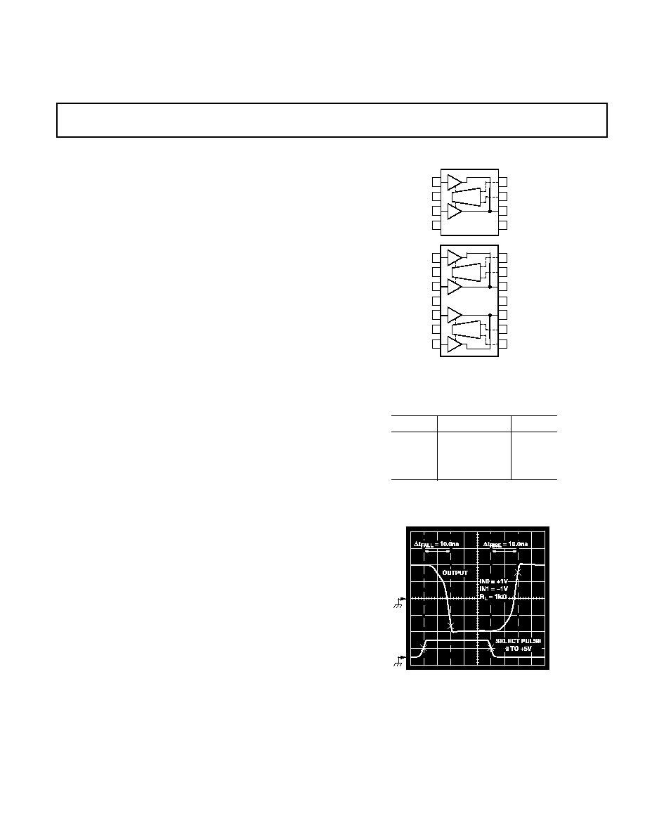
AD8180/AD8182*
FUNCTIONAL BLOCK DIAGRAM
1
2
3
4
8
7
6
5
AD8180
IN0
V
S
OUT
ENABLE
SELECT
GND
IN1
+V
S
DECODER
+1
+1
1
2
3
4
14
13
12
11
AD8182
V
S
OUT A
ENABLE
A
SELECT A
5
6
7
10
9
8
SELECT B
OUT B
ENABLE
B
DECODER
+1
+1
DECODER
+1
+1
IN0 A
GND
IN1 A
+V
S
IN1 B
GND
IN0 B
FEATURES
Fully Buffered Inputs and Outputs
Fast Channel Switching: 10 ns
High Speed
> 750 MHz Bandwidth (3 dB)
750 V/ s Slew Rate
Fast Settling Time of 14 ns to 0.1%
Low Power: 3.8 mA (AD8180), 6.8 mA (AD8182)
Excellent Video Specifications (R
L
1 k )
Gain Flatness of 0.1 dB Beyond 100 MHz
0.02% Differential Gain Error
0.02 Differential Phase Error
Low Glitch: < 35 mV
Low All-Hostile Crosstalk of 80 dB @ 5 MHz
High "OFF" Isolation of 90 dB @ 5 MHz
Low Cost
Fast Output Disable Feature for Connecting Multiple Devices
APPLICATIONS
Pixel Switching for "Picture-In-Picture"
Switching in LCD and Plasma Displays
Video Switchers and Routers
PRODUCT DESCRIPTION
The AD8180 (single) and AD8182 (dual) are high speed 2-to-1
multiplexers. They offer 3 dB signal bandwidth greater than
750 MHz along with slew rate of 750 V/
µ
s. With better than
80 dB of crosstalk and isolation, they are useful in many high
speed applications. The differential gain and differential phase
error of 0.02% and 0.02
°
, along with 0.1 dB flatness beyond
100 MHz make the AD8180 and AD8182 ideal for professional
video multiplexing. They offer 10 ns switching time making
them an excellent choice for pixel switching (picture-in-picture)
while consuming less than 3.8 mA (per 2:1 mux) on
±
5 V sup-
ply voltages.
Both devices offer a high speed disable feature allowing the
output to be configured into a high impedance state. This al-
lows multiple outputs to be connected together for cascading
stages while the "OFF" channels do not load the output bus.
They operate on voltage supplies of
±
5 V and are offered in 8-
and 14-lead plastic DIP and SOIC packages.
500mV
/DIV
5ns/DIV
Figure 1. AD8180/AD8182 Switching Characteristics
Table I. Truth Table
SELECT
ENABLE
OUTPUT
0
0
IN0
1
0
IN1
0
1
High Z
1
1
High Z
One Technology Way, P.O. Box 9106, Norwood, MA 02062-9106, U.S.A.
Tel: 781/329-4700
World Wide Web Site: http://www.analog.com
Fax: 781/326-8703
© Analog Devices, Inc., 2000
*Protected under U.S. Patent Number 5,955,908.

REV. B
2
AD8180/AD8182SPECIFICATIONS
AD8180A/AD8182A
Parameter
Conditions
Min
Typ
Max
Units
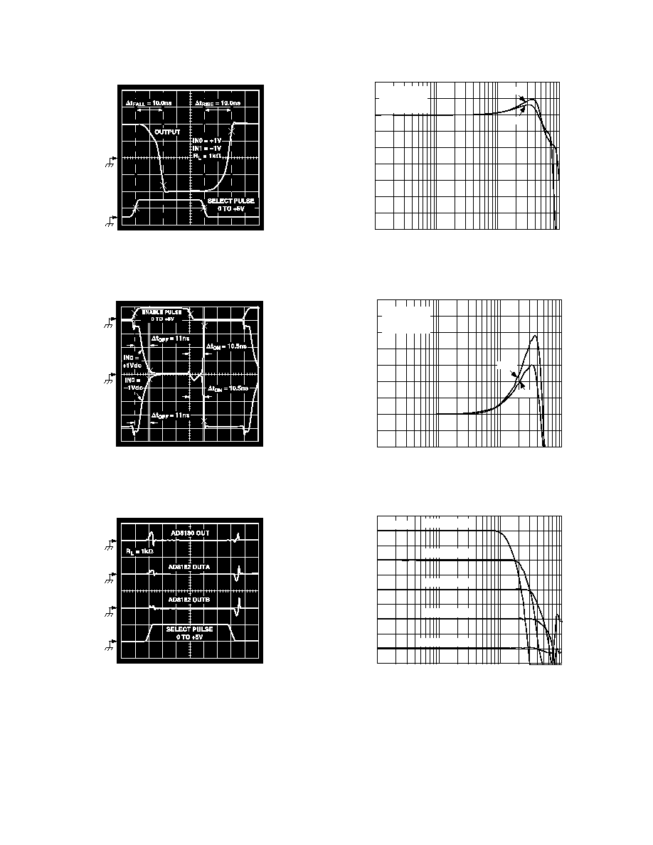
SWITCHING CHARACTERISTICS
Channel Switching Time
1
Channel-to-Channel
50% Logic to 10% Output Settling
IN0 = +1 V, IN1 = 1 V; R
L
= 1 k
5
ns
50% Logic to 90% Output Settling
IN0 = +1 V, IN1 = 1 V; R
L
= 1 k
10
ns
50% Logic to 99.9% Output Settling
IN0 = +1 V, IN1 = 1 V; R
L
= 1 k
14
ns
ENABLE to Channel ON Time
2
SEL = 0 or 1
50% Logic to 90% Output Settling
IN0 = +1 V, 1 V or IN1 = 1 V, +1 V; R
L
= 1 k
10.5
ns
ENABLE to Channel OFF Time
2
SEL = 0 or 1
50% Logic to 90% Output Settling
IN0 = +1 V, 1 V or IN1 = 1 V, +1 V; R
L
= 1 k
11
ns
Channel Switching Transient (Glitch)
3
All Inputs Are Grounded, R
L
= 1 k
±
25 /
±
35
mV
DIGITAL INPUTS
Logic "1" Voltage
SEL and
ENABLE Inputs
2.0
V
Logic "0" Voltage
SEL and
ENABLE Inputs
0.8
V
Logic "1" Input Current
SEL,
ENABLE = +4 V
10
200
nA
Logic "0" Input Current
SEL,
ENABLE = +0.4 V
2
3
µ
A
DYNAMIC PERFORMANCE
3 dB Bandwidth (Small Signal)
4
AD8180R
V
IN
= 50 mV rms, R
L
= 5 k
750
930
MHz
3 dB Bandwidth (Small Signal)
4
AD8182R
V
IN
= 50 mV rms, R
L
= 5 k
640
780
MHz
3 dB Bandwidth (Large Signal)
AD8180R
V
IN
= 1 V rms, R
L
= 5 k
120
150
MHz
3 dB Bandwidth (Large Si
AD8182R
V
IN
= 1 V rms, R
L
= 5 k
110
135
MHz
0.1 dB Bandwidth
4, 5
V
IN
= 50 mV rms, R
L
= 5 k
, R
S
= 0
100
MHz
AD8180R
V
IN
= 50 mV rms, R
L
= 1 k
5 k
, R
S
= 150
210
MHz
0.1 dB Bandwidth
4, 5
AD8182R
V
IN
= 50 mV rms, R
L
= 1 k
5 k
, R
S
= 125
210
MHz
Slew Rate
2 V Step
750
V/
µ
s
Settling Time to 0.1%
2 V Step
14
ns
DISTORTION/NOISE PERFORMANCE
Differential Gain
= 3.58 MHz, R
L
= 1 k
0.02
0.04
%
Differential Phase
= 3.58 MHz, R
L
= 1 k
0.02
0.04
Degrees
All Hostile Crosstalk
6
AD8180R
= 5 MHz, R
L
= 1 k
80
dB
= 30 MHz, R
L
= 1 k
65
dB
All Hostile Crosstalk
6
AD8182R
= 5 MHz, R
L
= 1 k
78
dB
= 30 MHz, R
L
= 1 k
63
dB
OFF Isolation
7
AD8180R
= 5 MHz, R
L
= 30
89
dB
OFF Isolation
7
AD8182R
= 5 MHz, R
L
= 30
93
dB
Voltage Noise
= 10 kHz30 MHz
4.5
nV/
Hz
Total Harmonic Distortion
C
= 10 MHz, V
O
= 2 V p-p, R
L
= 1 k
78
dBc
DC/TRANSFER CHARACTERISTICS
Voltage Gain
8
V
IN
=
±
1 V, R
L
= 2 k
0.982
V/V
V
IN
=
±
1 V, R
L
= 10 k
0.986
0.993
V/V
Input Offset Voltage
1
12
mV
T
MIN
to T
MAX
15
mV
Input Offset Voltage Matching
Channel-to-Channel
0.5
4
mV
Input Offset Drift
11
µ
V/
°
C
Input Bias Current
1
5
µ
A
T
MIN
to T
MAX
7
µ
A
Input Bias Current Drift
12
nA/
°
C
INPUT CHARACTERISTICS
Input Resistance
1
2.2
M
Input Capacitance
Channel Enabled (R Package)
1.5
pF
Channel Disabled (R Package)
1.5
pF
Input Voltage Range
±
3.3
V
OUTPUT CHARACTERISTICS
Output Voltage Swing
R
L
= 500
9
±
3.0
±
3.1
V
Short Circuit Current
30
mA
Output Resistance
Enabled
27
Disabled
1
10
M
Output Capacitance
Disabled (R Package)
1.7
pF
POWER SUPPLY
Operating Range
±
4
±
6
V
Power Supply Rejection Ratio
+PSRR
+V
S
= +4.5 V to +5.5 V, V
S
= 5 V
54
57
dB
Power Supply Rejection Ratio
PSRR
V
S
= 4.5 V to 5.5 V, +V
S
= +5 V
45
51
dB
Quiescent Current
All Channels "ON"
3.8/6.8
4.5/8
mA
T
MIN
to T
MAX
4.75/8.5
mA
All Channels "OFF"
1.3/2
2/3
mA
T
MIN
to T
MAX
2/3
mA
AD8182, One Channel "ON"
4
mA
OPERATING TEMPERATURE RANGE
40
+85
°
C
(@ T
A
= +25 C, V
S
= 5 V, R
L
= 2 k unless otherwise noted)
NOTES
1
ENABLE pin is grounded. IN0 = +1 V dc, IN1 = 1 V dc. SELECT input is driven with 0 V to +5 V pulse. Measure transition time from 50% of the SELECT input value
(+2.5 V) and 10% (or 90%) of the total output voltage transition from IN0 channel voltage (+1 V) to IN1 (1 V), or vice versa.
2
ENABLE pin is driven with 0 V to +5 V pulse (with 3 ns edges). State of SELECT input determines which channel is activated (i.e., if SELECT = Logic 0, IN0 is selected). Set
IN0 = +1 V dc, IN1 = 1 V dc, and measure transition time from 50% of
ENABLE pulse (+2.5 V) to 90% of the total output voltage change. In Figure 5,
t
OFF
is the disable
time,
t
ON
is the enable time.
3
All inputs are grounded. SELECT input is driven with 0 V to +5 V pulse. The outputs are monitored. Speeding the edges of the SELECT pulse increases the glitch magnitude
due to coupling via the ground plane. Removing the SELECT input termination will lower glitch, as does increasing R
L
.
4
Decreasing R
L
lowers the bandwidth slightly. Increasing C
L
lowers the bandwidth considerably (see Figure 19).
5
A resistor (R
S
) placed in series with the mux inputs serves to optimize 0.1 dB flatness, but is not required. Increasing output capacitance will increase peaking and reduce band-
width (see Figure 20.)
6
Select input which is not being driven (i.e., if SELECT is Logic 1, input activated is IN1); drive all other inputs with V
IN
= 0.707 V rms and monitor output at = 5 and 30 MHz.
R
L
= 1 k
(see Figure 13).
7
Mux is disabled (i.e.,
ENABLE = Logic 1) and all inputs are driven simultaneously with V
IN
= 0.446 V rms. Output is monitored at = 5 and 30 MHz. R
L
= 30
to simulate
R
ON
of one enabled mux within a system (see Figure 14). In this mode the output impedance is very high (typ 10 M
), and the signal couples across the package; the load imped-
ance determines the crosstalk.
8
Voltage gain decreases for lower values of R
L
. The resistive divider formed by the mux enabled output resistance (27
) and R
L
causes a gain which decreases as R
L
decreases
(i.e., the voltage gain is approximately 0.97 V/V (3% gain error) for R
L
= 1 k
).
9
Larger values of R
L
provide wider output voltage swings, as well as better gain accuracy. See Note 8.
Specifications subject to change without notice.
AD8180/AD8182
CAUTION
ESD (electrostatic discharge) sensitive device. Electrostatic charges as high as 4000 V readily
accumulate on the human body and test equipment and can discharge without detection.
Although the AD8180/AD8182 feature proprietary ESD protection circuitry, permanent damage
may occur on devices subjected to high energy electrostatic discharges. Therefore, proper ESD
precautions are recommended to avoid performance degradation or loss of functionality.
3
REV. B
ABSOLUTE MAXIMUM RATINGS
1
Supply Voltage . . . . . . . . . . . . . . . . . . . . . . . . . . . . . . . . . 12.6 V
Internal Power Dissipation
2
AD8180 8-Lead Plastic DIP (N) . . . . . . . . . . . . . . . . 1.3 Watts
AD8180 8-Lead Small Outline (R) . . . . . . . . . . . . . . 0.9 Watts
AD8182 14-Lead Plastic DIP (N) . . . . . . . . . . . . . . . 1.6 Watts
AD8182 14-Lead Small Outline (R) . . . . . . . . . . . . . 1.0 Watts
Input Voltage . . . . . . . . . . . . . . . . . . . . . . . . . . . . . . . . . . . . .
±
V
S
Output Short Circuit Duration . . . . . Observe Power Derating Curves
Storage Temperature Range
N and R Package . . . . . . . . . . . . . . . . . . . . . . 65
°
C to +125
°
C
Lead Temperature Range (Soldering 10 sec) . . . . . . . . . . +300
°
C
NOTES
1
Stresses above those listed under Absolute Maximum Ratings may cause perma-
nent damage to the device. This is a stress rating only; functional operation of the
device at these or any other conditions above those indicated in the operational
section of this specification is not implied. Exposure to absolute maximum rating
conditions for extended periods may affect device reliability.
2
Specification is for device in free air: 8-Lead Plastic DIP Package:
JA
= 90
°
C/W;
8-Lead SOIC Package:
JA
= 155
°
C/W; 14-Lead Plastic Package:
JA
= 75
°
C/W;
14-Lead SOIC Package:
JA
= 120
°
C/W, where P
D
= (T
J
T
A
)/
JA
.
ORDERING GUIDE
Temperature
Package
Package
Model
Range
Description
Option
AD8180AN
40
°
C to +85
°
C 8-Lead Plastic DIP
N-8
AD8180AR
40
°
C to +85
°
C 8-Lead SOIC
SO-8
AD8180AR-REEL
40
°
C to +85
°
C 13" Reel SOIC
SO-8
AD8180AR-REEL7 40
°
C to +85
°
C 7" Reel SOIC
SO-8
AD8182AN
40
°
C to +85
°
C 14-Lead Plastic DIP
N-14
AD8182AR
40
°
C to +85
°
C 14-Lead Narrow SOIC R-14
AD8182AR-REEL
40
°
C to +85
°
C 13" Reel SOIC
R-14
AD8182AR-REEL7 40
°
C to +85
°
C 7" Reel SOIC
R-14
AD8180-EB
Evaluation Board
AD8182-EB
Evaluation Board
MAXIMUM POWER DISSIPATION
The maximum power that can be safely dissipated by the
AD8180 and AD8182 is limited by the associated rise in junc-
tion temperature. The maximum safe junction temperature for
plastic encapsulated devices is determined by the glass transition
temperature of the plastic, approximately +150
°
C. Exceeding
this limit temporarily may cause a shift in parametric perfor-
mance due to a change in the stresses exerted on the die by the
package. Exceeding a junction temperature of +175
°
C for an
extended period can result in device failure.
While the AD8180 and AD8182 are internally short circuit
protected, this may not be sufficient to guarantee that the maxi-
mum junction temperature (+150
°
C) is not exceeded under all
conditions. To ensure proper operation, it is necessary to observe
the maximum power derating curves shown in Figures 2 and 3.
MAXIMUM POWER DISSIPATION Watts
AMBIENT TEMPERATURE C
2.0
1.5
0
50
90
40 30 20 10
0
10 20
30
50 60
70 80
40
1.0
0.5
8-LEAD PLASTIC DIP PACKAGE
8-LEAD SOIC PACKAGE
T
J
= +150 C
Figure 2. AD8180 Maximum Power Dissipation vs.
Temperature
AMBIENT TEMPERATURE C
2.5
2.0
0.5
50
90
40
MAXIMUM POWER DISSIPATION Watts
30 20 10 0
10 20
30 40 50
60
80
1.5
1.0
70
14-LEAD SOIC
14-LEAD
PLASTIC DIP PACKAGE
T
J
= +150 C
Figure 3. AD8182 Maximum Power Dissipation vs.
Temperature
WARNING!
ESD SENSITIVE DEVICE
4
REV. B
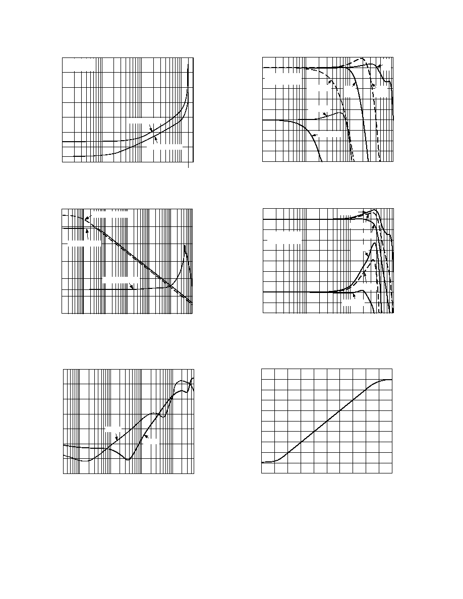
AD8180/AD8182Typical Performance Curves
500mV
/DIV
5ns/DIV
Figure 4. Channel Switching Characteristics
DUT OUT
250mV
/DIV
10ns/DIV
Figure 5. Enable and Disable Switching Characteristics
50mV
/DIV
25ns/DIV
Figure 6. Channel Switching Transient (Glitch)
7
0
1
2
3
4
5
6
V
IN
= 50mV rms
R
L
= 5k
R
S
= 0
1
NORMALIZED OUTPUT dB
8180R
8182R
1M
10M
100M
1G
FREQUENCY Hz
Figure 7. Small Signal Frequency Response
0.4
1.0
0.8
0.6
0.4
0.2
0.0
0.2
V
IN
= 50mV rms
R
L
= 5k
R
S
= 0
NORMALIZED FLATNESS dB
8180R
8182R
1M
10M
100M
1G
FREQUENCY Hz
Figure 8. Gain Flatness vs. Frequency
FREQUENCY Hz
1M
1G
10M
100M
3
0
27
3
6
9
12
15
18
21
24
INPUT/OUTPUT LEVEL dBV
V
IN
= 1.0V rms
V
IN
= 0.5V rms
V
IN
= 0.25V rms
V
IN
= 125mV rms
V
IN
= 62.5mV rms
R
L
= 1k
Figure 9. Large Signal Frequency Response
AD8180/AD8182
5
REV. B
FREQUENCY Hz
0.1M
1G
1M
10M
100M
10
20
110
30
40
50
60
70
80
90
100
CROSSTALK dB
V
IN
= 0.707V rms
R
L
= 1k
AD8182R
AD8180R
OUT A
OUT B
50
V
IN
50
1
3
5
7
50
AD8182
1k
1k
Figure 13. All-Hostile Crosstalk vs. Frequency
OFF ISOLATION dB
FREQUENCY Hz
0.03M
1G
0.1M
1M
10M
100M
10
20
110
30
40
50
60
70
80
90
100
ALL INPUTS = 0.446V rms
R
L
= 30
8180R OR
8182R
ENABLE
A = LOGIC 1
ENABLE
B = LOGIC 0
50
V
IN
50
8182R
ENABLE
A/B = LOGIC 1
AD8182
OUT A
OUT B
30
30
Figure 14. "OFF" Isolation vs. Frequency
FREQUENCY Hz
100
10
1
10
1M
100
1k
10k
100k
10M
VOLTAGE NOISE nV/ Hz
30M
Figure 15. Voltage Noise vs. Frequency
50mV
/DIV
5ns/DIV
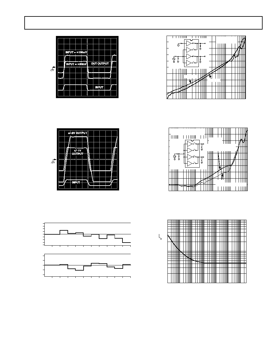
Figure 10. Small Signal Transient Response
500mV
/DIV
5ns/DIV
Figure 11. Large Signal Transient Response
DIFF GAIN %
0.020
0.015
0.010
0.005
0.000
0.005
0.010
0.015
0.020
0.02
0.01
0.00
0.01
0.02
DIFF PHASE Degrees
1
2
3
4
5
6
7
8
9
10
11
IRE
1
2
3
4
5
6
7
8
9
10
11
IRE
R
L
= 1k
NTSC
Figure 12. Differential Gain and Phase Error
AD8180/AD8182Typical Performance Curves
6
REV. B
FREQUENCY Hz
25
35
95
100k
200M
1M
10M
100M
55
65
75
85
45
150M
2ND HARMONIC
3RD HARMONIC
V
OUT
= 2V p-p
R
L
= 1k
HARMONIC DISTORTION dBc
Figure 16. Harmonic Distortion vs. Frequency
DISABLED OUTPUT AND INPUT IMPEDANCE
FREQUENCY Hz
31.6M
3.16M
31.6
1k
100M
10k
100k
1M
10M
31.6k
3.16k
316
316k
120
100
0
ENABLED OUTPUT IMPEDANCE
60
40
20
80
1G
Z
OUT
(DISABLED)
Z
IN
(ENABLED)
Z
OUT
(ENABLED)
Figure 17. Disabled Output and Input Impedance vs.
Frequency
PSRR dB
FREQUENCY MHz
0
20
0.03
500
0.1
1
10
100
40
60
10
30
50
70
+PSRR
PSRR
Figure 18. Power Supply Rejection vs. Frequency
NORMALIZED OUTPUT dB
+1
0
9
1
2
3
4
5
6
7
8
0.4
+0.1
0
0.1
0.2
0.3
NORMALIZED FLATNESS dB
V
IN
= 500mV rms
R
L
= 5k
C
L
=
0pF
C
L
=
10pF
C
L
=
33pF
C
L
= 100pF
C
L
= 100pF
C
L
= 33pF
10M
100M
1G
4M
40M
400M
FREQUENCY Hz
1M
Figure 19. Frequency Response vs. Capacitive Load
NORMALIZED OUTPUT dB
+1
0
9
1
2
3
4
5
6
7
8
0.4
0.6
0.4
0.2
0
0.2
NORMALIZED FLATNESS dB
V
IN
= 50mV rms
R
L
= 5k
R
S
= 0
R
S
= 75
0.8
1.0
R
S
= 150
R
S
= 0
R
S
= 75
R
S
= 150
10M
100M
40M
FREQUENCY Hz
400M
1G
4M
1M
Figure 20. Frequency Response vs. Input Series Resistance
INPUT VOLTAGE Volts
5
1
5
5
5
4
3
2
1
0
1
2
3
4
4
0
2
4
2
1
3
3
OUTPUT VOLTAGE Volts
Figure 21. Output Voltage vs. Input Voltage, R
L
= 1 k
AD8180/AD8182
7
REV. B
for R
L
> 10 k
. For heavier loads, the dc gain is approximately
that of the voltage divider formed by the output impedance of
the mux (typically 27
) and R
L
.
High speed disable clamp circuits at the bases of Q5Q8 (not
shown) allow the buffers to turn off quickly and cleanly without
dissipating much power once off. Moreover, these clamps shunt
displacement currents flowing through the junction capacitances
of Q1Q4 away from the bases of Q5Q8 and to ac ground
through low impedances. The two-pole high pass frequency
response of the T switch formed by these clamps is a significant
improvement over the one-pole high pass response of a simple
series CMOS switch. As a result, board and package parasitics,
especially stray capacitance between inputs and outputs may
limit the achievable crosstalk and off isolation.
LAYOUT CONSIDERATIONS:
Realizing the high speed performance attainable with the
AD8180 and AD8182 requires careful attention to board layout
and component selection. Proper RF design techniques and low
parasitic component selection are mandatory.
Wire wrap boards, prototype boards, and sockets are not recom-
mended because of their high parasitic inductance and capaci-
tance. Instead, surface-mount components should be soldered
directly to a printed circuit board (PCB). The PCB should have
a ground plane covering all unused portions of the component
side of the board to provide a low impedance ground path. The
ground plane should be removed from the area near input and
output pins to reduce stray capacitance.
Chip capacitors should be used for supply bypassing. One end
of the capacitor should be connected to the ground plane and
the other within 1/4 inch of each power pin. An additional large
(4.7
µ
F10
µ
F) tantalum capacitor should be connected in
parallel with each of the smaller capacitors for low impedance
supply bypassing over a broad range of frequencies.
Signal traces should be as short as possible. Stripline or micros-
trip techniques should be used for long signal traces (longer
than about 1 inch). These should be designed with a character-
istic impedance of 50
or 75
and be properly terminated at
the end using surface mount components.
Careful layout is imperative to minimize crosstalk. Guards
(ground or supply traces) must be run between all signal traces
to limit direct capacitive coupling. Input and output signal lines
should fan out away from the mux as much as possible. If mul-
tiple signal layers are available, a buried stripline structure hav-
ing ground plane above, below, and between signal traces will
have the best crosstalk performance.
Return currents flowing through termination resistors can also
increase crosstalk if these currents flow in sections of the finite-
impedance ground circuit that is shared between more than one
input or output. Minimizing the inductance and resistance of the
ground plane can reduce this effect, but further care should be
taken in positioning the terminations. Terminating cables directly
at the connectors will minimize the return current flowing on the
board, but the signal trace between the connector and the mux will
look like an open stub and will degrade the frequency response.
Moving the termination resistors close to the input pins will im-
prove the frequency response, but the terminations from neigh-
boring inputs should not have a common ground return.
THEORY OF OPERATION
The AD8180 and AD8182 video multiplexers are designed for
fast-switching (10 ns) and wide bandwidth (> 750 MHz). This
performance is attained with low power dissipation (3.8 mA per
active channel) through the use of proprietary circuit techniques
and a dielectrically-isolated complementary bipolar process.
These devices have a fast disable function that allows the out-
puts of several muxes to be wired in parallel to form a larger mux
with little degradation in switching time. The low disabled output
capacitance (1.7 pF) of these muxes helps to preserve the system
bandwidth in larger matrices. Unlike earlier CMOS switches,
the switched open-loop buffer architecture of the AD8180 and
AD8182 provides a unidirectional signal path with minimal switch-
ing glitches and constant, low input capacitance. Since the input
impedance of these muxes is nearly independent of the load imped-
ance and the state of the mux, the frequency response of the ON
channels in a large switch matrix is not affected by fanout.
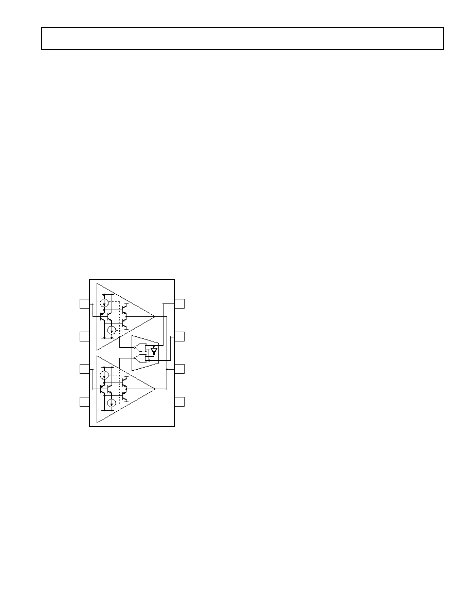
Figure 22 shows a block diagram and simplified schematic of the
AD8180, which contains two switched buffers (S0 and S1) that
share a common output. The decoder logic translates TTL-
compatible logic inputs (SELECT and
ENABLE) to internal,
differential ECL levels for fast, low-glitch switching. The SELECT
input determines which of the two buffers is enabled, unless the
ENABLE input is HIGH, in which case both buffers are disabled
and the output is switched to a high impedance state.
Q5
Q7
Q3
Q1
S0
I1
I3
Q6
Q8
Q4
Q2
S1
I2
I4
DECODER
AD8180
1
2
3
4
IN0
GND
IN1
+V
S
8
7
6
5
V
S
OUT
ENABLE
SELECT
Figure 22. Block Diagram and Simplified Schematic of the
AD8180 Multiplexer
Each open-loop buffer is implemented as a complementary
emitter follower that provides high input impedance, symmetric
slew rate and load drive, and high output-to-input isolation due to
its
2
current gain. The selected buffer is biased ON by fast
switched current sources that allow the buffer to turn on quickly.
Dedicated flatness circuits, combined with the open-loop architec-
ture of the AD8180 and AD8182, keep peaking low (typically
< 1 dB) when driving high capacitive loads, without the need for
external series resistors at the input or output. If better flatness
response is desired, an input series resistance (R
S
) may be used
(refer to Figure 20), although this will increase crosstalk. The dc
gain of the AD8180 and AD8182 is almost independent of load
AD8180/AD8182
8
REV. B
APPLICATIONS
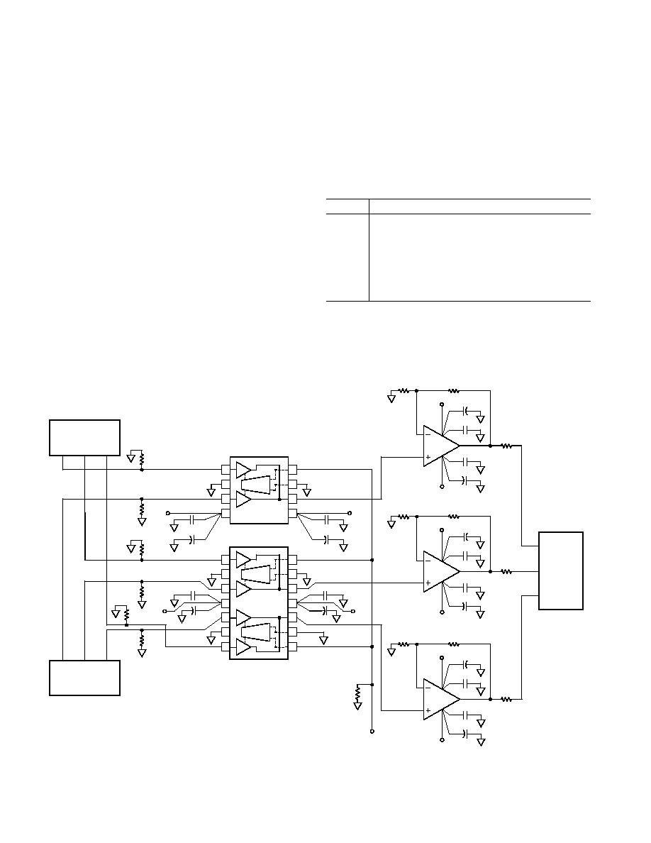
Multiplexing two RGB Video Sources
A common video application requires two RGB sources to be
multiplexed together before the selected signal is applied to a
monitor. Typically one source would be the PC's normal output,
the second source might be a specialized source such as MPEG
video. Figure 23 shows how such a circuit could be realized
using the AD8180 and AD8182 and three current feedback op
amps. The video inputs to the multiplexers are terminated with
75
resistors. This has the effect of halving the signal amplitude
of the applied signals.
Because all three multiplexers are permanently active, the
ENABLE pins are tied permanently low. The three SELECT
pins are tied together and this signal is used to select the source.
In order to drive a 75
back terminated load (R
L
= 150
), the
multiplexer outputs are buffered using the AD8001 current feed-
back op amp. A gain of two compensates for the signal halving by
the AD8001 output back termination resistor so that the system
has an overall gain of unity.
If lower speed and crosstalk can be tolerated, either of the triple
op amps, AD8013 or AD8073, can replace the three AD8001 op
amps in the above circuit. Because both devices have bandwidths
in the 100 MHz to 140 MHz range at a gain of +2, these ampli-
fiers will dominate the frequency response of the circuit.
With no signal present, the total quiescent current of the cir-
cuit in Figure 23 is 25.6 mA (3.8 mA + 6.8 mA + 3
×
5 mA), or
about 8.5 mA per channel. If either the AD8013 or AD8073
are used, the quiescent current will decrease to about 6.5 mA
per channel.
To reduce power consumption further, three AD8011 single
op amps can be used. With a quiescent current of 1 mA, this
will reduce the per channel quiescent current to about 4.5 mA.
Table II. Amplifier Options for RGB Multiplexer
Op Amp Comments
AD8001
Highest Bandwidth, 440 MHz (G = +2), I
SY
= 5 mA
AD8011
Lower Power Consumption, Bandwidth (G = +2) =
210 MHz, I
SY
= 1 mA
AD8013
Triple Op Amp, Bandwidth (G = +2) = 140 MHz,
I
SY
= 3.4 mA
AD8073
Lower Power Triple Op Amp, Bandwidth (G = +2) =
100 MHz, I
SY
= 3.5 mA
8
7
6
5
ENABLE
ENABLE
A
V
S
ENABLE
B
V
S
+V
S
0.1 F
10 F
0.1 F
10 F
0.1 F
+V
S
+
75
75
75
75
75
75
R
G
B
COMPUTER
GRAPHICS
R
G
B
+
+V
S
0.1 F
10 F
75
681
V
S
+
10 F
0.1 F
+
+V
S
0.1 F
10 F
75
681
681
V
S
+
10 F
0.1 F
+
+V
S
0.1 F
10 F
75
681
V
S
+
10 F
0.1 F
SELECT
MONITOR
1
2
3
4
AD8180
+1
+1
1
2
3
4
14
13
12
11
AD8182
5
6
7
10
9
8
DECODER
+1
+1
DECODER
+1
+1
+
+
MPEG
R
TERM
AD8001
681
AD8001
681
AD8001
R
G
B
0.1 F
10 F
+
10 F
DECODER
Figure 23. Multiplexing Two Component Video Sources
AD8180/AD8182
9
REV. B
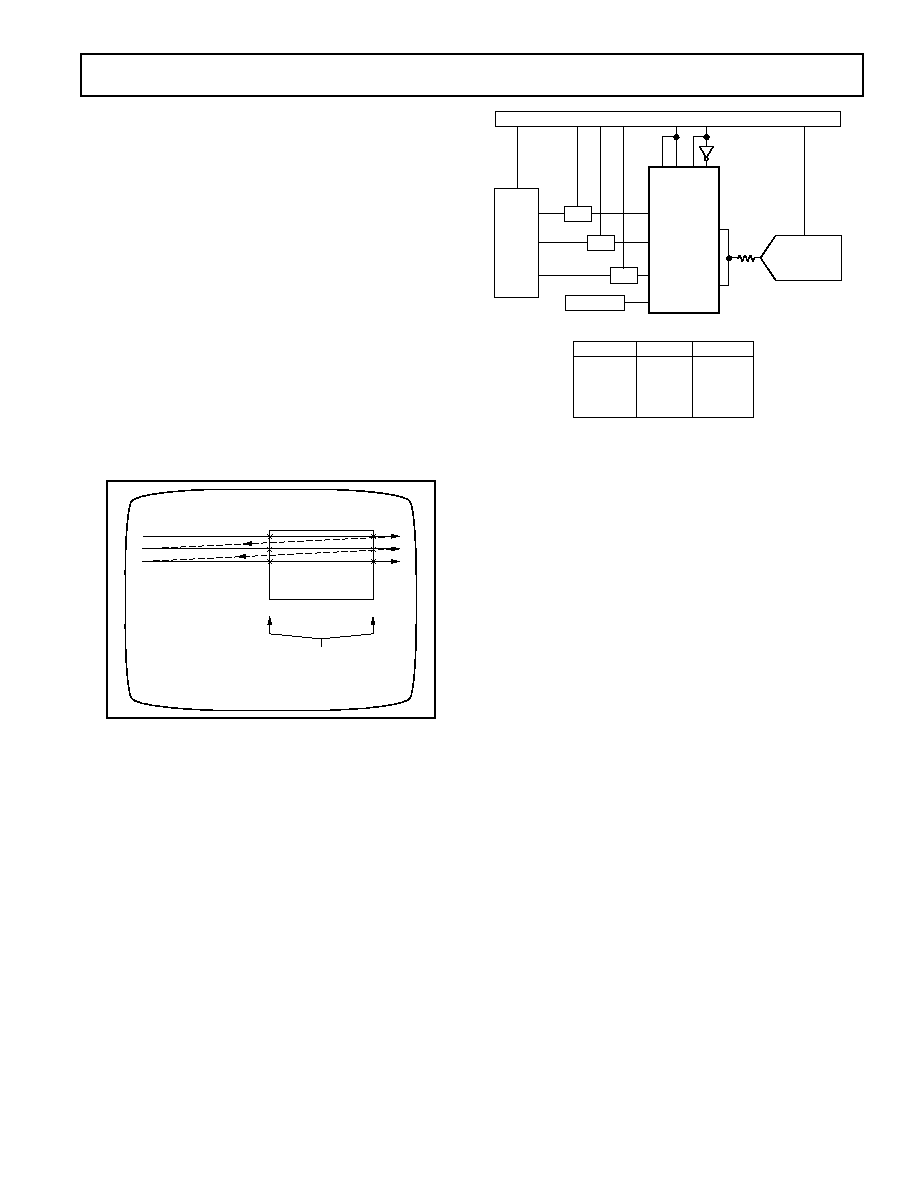
Picture-in-Picture or Pixel Switching
Many high end display systems require simultaneous display of
two video pictures (from two different sources) on one screen.
Video conferencing is one such example. In this case the remote
site might be displayed as the main picture with a picture of the
local site "inset" for monitoring purposes. The circuit in Fig-
ure 23 could also be used to implement this "picture-in-picture"
application.
Implementing a picture-in-picture algorithm is difficult for
several reasons. Both sources are being displayed simultaneously
(i.e., during the same frame), both sources are in real time, and
both must be synchronized. Figure 24 shows the raster scan-
ning that takes place in all monitors. During every horizontal
scan that includes part of the inset, the source must be switched
twice (i.e., from main to inset and from inset to main). To avoid
screen artifacts, it is critical that switching is clean and fast. The
AD8180 and AD8182, in the above application, switch and
settle to 0.1% accuracy in 14 ns. We quadratically add this
value to the 10 ns settling time of the AD8001, and get an over-
all settling time of 17.2 ns. This yields a sharp, artifact-free
border between the inset and the main video.
INSET VIDEO
MULTIPLEXER MUST SWITCH
CLEANLY ON EACH CROSSING
MAIN VIDEO
Figure 24. "Picture-in-Picture," Pixel Switching
Color Document Scanner
Figure 25 shows a block diagram of a Color Document Scan-
ner. Charge Coupled Devices (CCDs) find widespread use in
scanner applications. A monochrome CCD delivers a serial
stream of voltage levels, each level being proportional to the
light shining on that cell. In the case of the color image scanner
shown, there are three output streams, representing red, green
and blue. Interlaced with the stream of voltage levels is a voltage
representing the reset level (or black level) of each cell. A Corre-
lated Double Sampler (CDS) subtracts these two voltages from
each other in order to eliminate the relatively large offsets which
are common with CCDs.
CONTROL AND TIMING
AD876 8/10-BIT
20MSPS
A/D
AD8182
OUT A
OUT B
CDS
CDS
CDS
REFERENCE
R
G
B
C
C
D
IN0 A
IN1 A
IN1 B
IN0 B
100
4:1 MUX TRUTH TABLE
SEL A, SEL B
ENA
, ENB
OUTA, OUTB
0
0
1
1
0
1
0
1
IN0A
IN0B
IN1A
IN1B
EN
A
EN
B
SEL A
SEL B
Figure 25. Color Document Scanner
The next step in the data acquisition process involves digitizing
the three signal streams. Assuming that the analog to digital
converter chosen has a fast enough sample rate, multiplexing
the three streams into a single ADC is generally more eco-
nomic than using one ADC per channel. In the example
shown, we use the two 2-to-1 multiplexers in the AD8182 to
create a 4-to-1 multiplexer. The enable control pins on the
multiplexers allow the outputs to be wired directly together.
Because of its high bandwidth, the AD8182 is capable of driv-
ing the switched capacitor input stage of the AD876 without
additional buffering. In addition to having the required the
bandwidth, it is necessary to consider the settling time of the
multiplexer. In this case, the ADC has a sample rate of 20 MHz
which corresponds to a sampling period of 50 ns. Typically,
one phase of the sampling clock is used for conversion (i.e., all
levels are held steady) and the other phase is used for switch-
ing and settling to the next channel. Assuming a 50% duty cycle,
the signal chain must settle within 25 ns. With a settling time to
0.1% of 14 ns, the multiplexer easily satisfies this criterion.
In the example shown, the fourth (spare) channel of the
AD8182 is used to measure a reference voltage. This voltage
would probably be measured less frequently than the R, G and
B signals. Multiplexing a reference voltage offers the advantage
that any temperature drift effects caused by the multiplexer
will equally impact the reference voltage and the to-be-
measured signals. If the fourth channel is unused, it is good
design practice to tie this input to ground.
AD8180/AD8182
10
REV. B
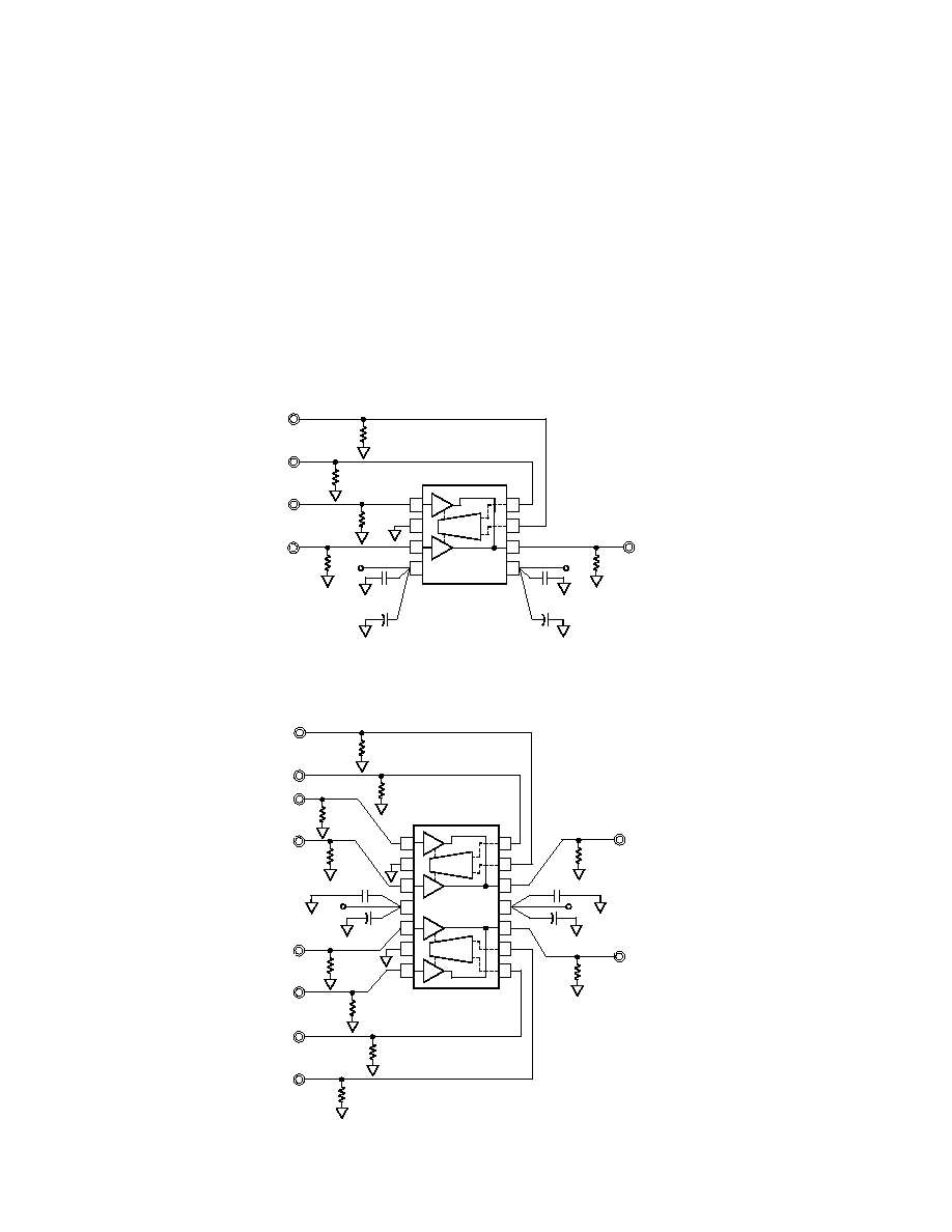
EVALUATION BOARD
Evaluation boards for the AD8180R and AD8182R are available
which have been carefully laid out and tested to demonstrate the
specified high speed performance of the devices. Figure 26 and
Figure 27 show the schematics of the AD8180 and AD8182
evaluation boards respectively. For ordering information, please
refer to the Ordering Guide.
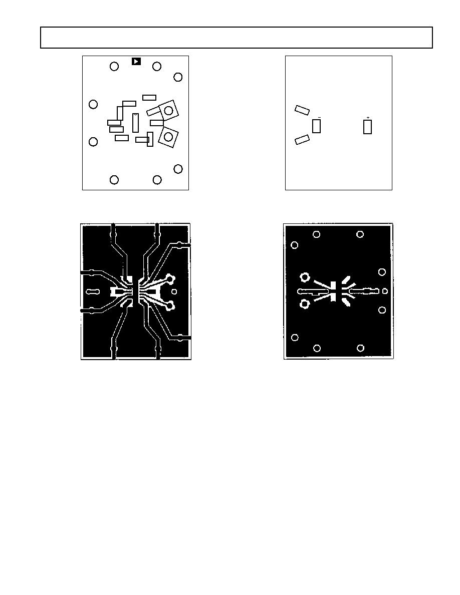
Because the footprint of the AD8180 fits directly on to that of
the AD8182, one board layout can be used for both devices. In the
case of the AD8180, only the top half of the board is populated.
Figure 28 shows the silkscreen of the component side and Fig-
ure 30 shows the silkscreen of the solder side. Figures 29 and 31
show the layout of the component side and solder side respectively.
The evaluation board is provided with 49.9
termination resis-
tors on all inputs. This is to allow the performance to be evalu-
ated at very high frequencies where 50
termination is most
popular. To use the evaluation board in video applications, the
termination resistors should be replaced with 75
resistors.
The multiplexer outputs are loaded with 4.99 k
resistors. In
order to avoid large gain errors, these load resistors should be
greater than or equal to 1 k
. For connection to external instru-
ments, oscilloscope scope probe adapters are provided. This
allows direct connection of FET probes to the board. For verifi-
cation of data sheet specifications, use of FET probes with a
bandwidth > 1 GHz is recommended because of their low input
capacitance. The probe adapters used on the board have the
same footprint as SMA, SMB and SMC type connectors allow-
ing easy replacement if necessary.
8
7
6
5
+V
S
C4
10 F
C1
0.1 F
R10
49.9
1
2
3
4
AD8180R
DECODER
+1
+1
+
R1
49.9
IN1
IN0
SELECT
R9
49.9
ENABLE
R8
49.9
+
V
S
C3
10 F
C2
0.1 F
R7
4.99k
OUT
(SCOPE PROBE
ADAPTER)
UNLESS OTHERWISE NOTED, CONNECTORS ARE SMA TYPE
Figure 26. AD8180R Evaluation Board
V
S
+
+V
S
C1
0.1 F
C4
10 F
R10
49.9
1
2
3
4
14
13
12
11
AD8182R
5
6
7
10
9
8
DECODER
+1
+1
DECODER
+1
+1
R1
49.9
IN1 A
IN0 A
R9
49.9
SELECT A
R8
49.9
ENABLE
A
R2
49.9
IN1 B
IN0 B
R3
49.9
R4
49.9
SELECT B
R5
49.9
ENABLE
B
+
C3
10 F
C2
0.1 F
OUTB
(SCOPE PROBE
ADAPTER)
OUTA
(SCOPE PROBE
ADAPTER)
R6
4.99k
R7
4.99k
UNLESS OTHERWISE NOTED, CONNECTORS ARE SMA TYPE
Figure 27. AD8182R Evaluation Board
AD8180/AD8182
11
REV. B
C1
ANALOG
DEVICES
AD8180/82
EVALUATION
BOARD
J1
IN0A
J10
SEL A
J2
IN1A
J3
IN1B
IN0B
J4
J9
J8
EN A
R10
R1
U1
R2
R3
V+
V
SEL B
J5
J6
EN B
A
B
C2
R5
J7
R9
R8
R4
Figure 28. Component Side Silkscreen
Figure 29. Board Layout (Component Side)
C3
C4
R7
R6
Figure 30. Solder Side Silkscreen
Figure 31. Board Layout (Solder Side)
NOTES
1. AD8180R/AD8182R Evaluation Board inputs are configured
with 50
impedance striplines. This FR4 board type has the
following stripline dimensions: 60-mil width, 12-mil gap
between center conductor and outside ground plane "is-
lands," and 62-mil board thickness.
2. Several types of SMA connectors can be mounted on this
board: the side-mount type, which can be easily installed at
the edges of the board, and the top-mount type, which is
placed on top. When using the top-mount SMA connector, it
is recommended that the stripline on the outside 1/8" of the
board edge be removed with an X-Acto blade as this unused
stripline acts as an open stub, which could degrade the small-
signal frequency response of the mux.
3. Input termination resistor placement on the evaluation board
is critical to reducing crosstalk. Each termination resistor is
oriented so that ground return currents flow counterclock-
wise to a ground plane "island." Although the direction of
this ground current flow is arbitrary, it is important that no
two input or output termination resistors share a connection
to the same ground "island."
AD8180/AD8182
12
REV. B
C2182a01/00 (rev. B)
PRINTED IN U.S.A.
12
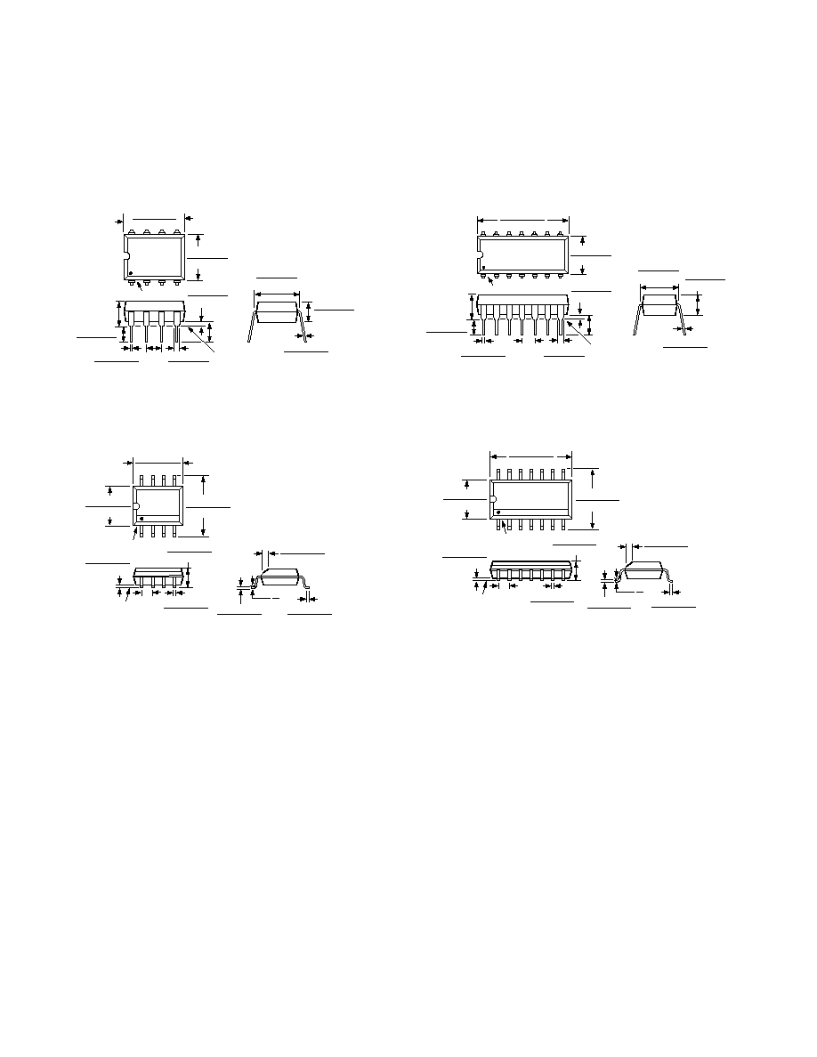
OUTLINE DIMENSIONS
Dimensions shown in inches and (mm).
8-Lead Plastic DIP
(N-8)
8
1
4
5
0.430 (10.92)
0.348 (8.84)
0.280 (7.11)
0.240 (6.10)
PIN 1
SEATING
PLANE
0.022 (0.558)
0.014 (0.356)
0.060 (1.52)
0.015 (0.38)
0.210 (5.33)
MAX
0.130
(3.30)
MIN
0.070 (1.77)
0.045 (1.15)
0.100
(2.54)
BSC
0.160 (4.06)
0.115 (2.93)
0.325 (8.25)
0.300 (7.62)
0.015 (0.381)
0.008 (0.204)
0.195 (4.95)
0.115 (2.93)
8-Lead Plastic SOIC
(SO-8)
0.1968 (5.00)
0.1890 (4.80)
8
5
4
1
0.2440 (6.20)
0.2284 (5.80)
PIN 1
0.1574 (4.00)
0.1497 (3.80)
0.0688 (1.75)
0.0532 (1.35)
SEATING
PLANE
0.0098 (0.25)
0.0040 (0.10)
0.0192 (0.49)
0.0138 (0.35)
0.0500
(1.27)
BSC
0.0098 (0.25)
0.0075 (0.19)
0.0500 (1.27)
0.0160 (0.41)
8°
0°
0.0196 (0.50)
0.0099 (0.25)
x 45°
14-Lead Plastic DIP
(N-14)
14
1
7
8
0.795 (20.19)
0.725 (18.42)
0.280 (7.11)
0.240 (6.10)
PIN 1
0.325 (8.25)
0.300 (7.62)
0.015 (0.381)
0.008 (0.204)
0.195 (4.95)
0.115 (2.93)
SEATING
PLANE
0.022 (0.558)
0.014 (0.356)
0.060 (1.52)
0.015 (0.38)
0.210 (5.33)
MAX
0.130
(3.30)
MIN
0.070 (1.77)
0.045 (1.15)
0.100
(2.54)
BSC
0.160 (4.06)
0.115 (2.93)
14-Lead SOIC
(R-14)
14
8
7
1
0.3444 (8.75)
0.3367 (8.55)
0.2440 (6.20)
0.2284 (5.80)
0.1574 (4.00)
0.1497 (3.80)
PIN 1
SEATING
PLANE
0.0098 (0.25)
0.0040 (0.10)
0.0192 (0.49)
0.0138 (0.35)
0.0688 (1.75)
0.0532 (1.35)
0.0500
(1.27)
BSC
0.0099 (0.25)
0.0075 (0.19)
0.0500 (1.27)
0.0160 (0.41)
8°
0°
0.0196 (0.50)
0.0099 (0.25)
x 45°