 | ÐлекÑÑоннÑй компоненÑ: AD8183ARU | СкаÑаÑÑ:  PDF PDF  ZIP ZIP |
Äîêóìåíòàöèÿ è îïèñàíèÿ www.docs.chipfind.ru

REV. 0
Information furnished by Analog Devices is believed to be accurate and
reliable. However, no responsibility is assumed by Analog Devices for its
use, nor for any infringements of patents or other rights of third parties
which may result from its use. No license is granted by implication or
otherwise under any patent or patent rights of Analog Devices.
a
AD8183/AD8185*
One Technology Way, P.O. Box 9106, Norwood, MA 02062-9106, U.S.A.
Tel: 781/329-4700
World Wide Web Site: http://www.analog.com
Fax: 781/326-8703
© Analog Devices, Inc., 1999
*Patents pending.
380 MHz, 25 mA,
Triple 2:1 Multiplexers
FEATURES
Fully Buffered Inputs and Outputs
Fast Channel-to-Channel Switching: 15 ns
High Speed
380 MHz Bandwidth (3 dB) 200 mV p-p
310 MHz Bandwidth (3 dB) 2 V p-p
1000 V/ s Slew Rate G = +1, 2 V Step
1150 V/ s Slew Rate G = +2, 2 V Step
Fast Settling Time of 15 ns to 0.1%
Low Power: 25 mA
Excellent Video Specifications (R
L
= 150 )
Gain Flatness of 0.1 dB to 90 MHz
0.01% Differential Gain Error
0.02 Differential Phase Error
Low All-Hostile Crosstalk 84 dB @ 5 MHz
54 dB @ 50 MHz
Low Channel-to-Channel Crosstalk 56 dB @ 100 MHz
High "OFF" Isolation of 100 dB @ 10 MHz
Low Cost
Fast High Impedance Output Disable Feature for
Connecting Multiple Devices
APPLICATIONS
Pixel Switching for "Picture-In-Picture"
Switching RGB in LCD and Plasma Displays
RGB Video Switchers and Routers
PRODUCT DESCRIPTION
The AD8183 (G = +1) and AD8185 (G = +2) are high speed
triple 2:1 multiplexers. They offer 3 dB signal bandwidth up to
380 MHz, along with slew rate of 1000 V/
µ
s. With better than
90 dB of channel-to-channel crosstalk and isolation at 10 MHz,
they are useful in many high-speed applications. The differential
gain and differential phase errors of 0.01% and 0.02
°
respectively,
along with 0.1 dB flatness to 90 MHz make the AD8183 and
AD8185 ideal for professional video and RGB multiplexing. They
offer 15 ns channel-to-channel switching time, making them
an excellent choice for switching video signals, while consuming
less than 25 mA on
±
5 V supply voltages.
Both devices offer a high speed disable feature that can set the
output into a high impedance state. This allows the building of
larger input arrays while minimizing "OFF" channel output
loading. They operate on voltage supplies of
±
5 V and are offered
in a 24-lead TSSOP package.
Table I. Truth Table
SEL
A/B
OE
OUT
0
0
INA
1
0
INB
0
1
High Z
1
1
High Z
200mV
2ns
V
O
= 1.4V STEP
R
L
= 150
1.4V
1.2V
1.0V
0.8V
0.6V
0.4V
0.2V
0.0V
Figure 1. AD8185 Pulse Response; R
L
= 150
FUNCTIONAL BLOCK DIAGRAM
AD8183/AD8185
IN0B
GND
IN1B
GND
IN2B
IN0A
DGND
IN1A
GND
V
EE
V
CC
IN2A
1
2
3
4
5
6
7
8
9
10
11
12
V
CC
DVCC
V
EE
OUT2
V
CC
V
CC
OE
SEL
A
/B
V
CC
OUT1
V
EE
OUT0
24
23
22
21
20
19
18
17
16
15
14
13
SELECT
DISABLE
0
1
2

REV. 0
2
AD8183/AD8185SPECIFICATIONS
(T
A
= 25 C, V
S
= 5 V, R
L
= 1 k unless otherwise noted)
Parameter
Condition
Min
Typ
Max
Unit
DYNAMIC PERFORMANCE
3 dB Bandwidth (Small Signal)
V
OUT
= 200 mV p-p
250/300
590/360
MHz
3 dB Bandwidth (Small Signal)
V
OUT
= 200 mV p-p, R
L
= 150
200/250
380/320
MHz
3 dB Bandwidth (Large Signal)
V
OUT
= 2 V p-p
250/300
530/350
MHz
3 dB Bandwidth (Large Si
V
OUT
= 2 V p-p, R
L
= 150
200/250
310/300
MHz
0.1 dB Bandwidth
V
OUT
= 200 mV p-p
90/60
MHz
V
OUT
= 200 mV p-p, R
L
= 150
100/160
MHz
Slew Rate
2 V Step
1000/1150
V/
µ
s
Settling Time to 0.1%
2 V Step, R
L
= 150
15
ns
NOISE/DISTORTION PERFORMANCE
Differential Gain
NTSC or PAL, 150
0.01
%
Differential Phase
NTSC or PAL, 150
0.02
Degrees
All-Hostile Crosstalk, RTI
= 5 MHz, AD8185: R
L
= 150
84/72
dB
= 50 MHz, AD8185: R
L
= 150
54/50
dB
Channel-to-Channel Crosstalk, RTI
= 100 MHz, AD8185: R
L
= 150
56/54
dB
OFF Isolation
= 10 MHz, R
L
= 150
100
dB
Voltage Noise, RTI
= 10 kHz to 30 MHz
28/15
nV/
Hz
DC PERFORMANCE
Voltage Gain Error
No Load
0.20
0.25/0.85
%
Input Offset Voltage, RTI
5
25/40
mV
T
MIN
to T
MAX
10
mV
Input Offset Voltage Matching, RTI
Channel-to-Channel
1
25/40
mV
Input Offset Drift, RTI
15
µ
V/
°
C
Input Bias Current
6/10
10/15
µ
A
INPUT CHARACTERISTICS
Input Resistance
4/1
8/5
M
Input Capacitance
Channel Enabled
1
pF
Channel Disabled
1.5
pF
Input Voltage Range
±
3.0/
±
1.5
V
OUTPUT CHARACTERISTICS
Output Voltage Swing
R
L
= 1 k
±
2.90
±
3.25
V
R
L
= 150
±
2.65
±
2.95
V
Short Circuit Current
60
mA
Output Resistance
Enabled
0.3
Disabled
4/1
8/3
M
Output Capacitance
Disabled
4/6.5
pF
POWER SUPPLY
Operating Range
±
4.5
±
5.5
V
Power Supply Rejection Ratio
+PSRR +V
S
= +4.5 V to +5.5 V, V
S
= 5 V
58/62
66/72
dB
Power Supply Rejection Ratio
PSRR V
S
= 4.5 V to 5.5 V, +V
S
= +5 V
52/60
56/68
dB
Quiescent Current
All Channels "ON"
25
30
mA
All Channels "OFF"
3/7
5/10
mA
T
MIN
to T
MAX
; All Channels "ON"
25
mA
SWITCHING CHARACTERISTICS
Switch Time
Channel-to-Channel
50% Logic to 50% Output Settling
IN0 = +1 V, IN1 = 1 V
15
ns
ENABLE to Channel ON Time
50% Logic to 50% Output Settling
INPUT = 1 V
20
ns
ENABLE to Channel OFF Time
50% Logic to 50% Output Settling
INPUT = 1 V
45
ns
Channel Switching Transient (Glitch)
All Inputs Grounded
50/70
mV
DIGITAL INPUTS
Logic "1" Voltage
SEL
A/B and OE Inputs
2.0
V
Logic "0" Voltage
SEL
A/B and OE Inputs
0.8
V
Logic "1" Input Current
SEL
A/B and OE = 4 V
10
nA
Logic "0" Input Current
SEL
A/B and OE = 0.4 V
0.5
µ
A
OPERATING TEMPERATURE RANGE
Temperature Range
Operating (Still Air)
40
+85
°
C
JA
Operating (Still Air)
128
°
C/W
JC
Operating
42
°
C/W
Specifications subject to change without notice.
REV. 0
AD8183/AD8185
3
ABSOLUTE MAXIMUM RATINGS
1
Supply Voltage . . . . . . . . . . . . . . . . . . . . . . . . . . . . . . . . . 12.0 V
DVCC to V
CC
. . . . . . . . . . . . . . . . . . . . . . . . . . . . . . . . . .
±
0.2 V
Internal Power Dissipation
2, 3
AD8183/AD8185 24-Lead TSSOP (RU) . . . . . . . . . . . . . 1 W
Input Voltage
IN0A, IN0B, IN1A, IN1B, IN2A, IN2B . . . . . V
EE
V
IN
V
CC
SELECT
A/B, OE . . . . . . . . . . . . . . . . . . DGND
V
IN
V
CC
Output Short Circuit Duration . . . . . . . . . . . . . . . . . . . Indefinite
3
Storage Temperature Range . . . . . . . . . . . . . . . 65
°
C to +150
°
C
Lead Temperature Range (Soldering 10 sec) . . . . . . . . . . . 300
°
C
NOTES
1
Stresses above those listed under Absolute Maximum Ratings may cause perma-
nent damage to the device. This is a stress rating only; functional operation of the
device at these or any other conditions above those indicated in the operational
section of this specification is not implied. Exposure to absolute maximum rating
conditions for extended periods may affect device reliability.
2
Specification is for device in free air (T
A
= 25
°
C).
3
24-lead plastic TSSOP;
JA
= 128
°
C/W. Maximum internal power dissipation (P
D
)
should be derated for ambient temperature (T
A
) such that P
D
< (150
°
CT
A
)/
JA
.
ORDERING GUIDE
Temperature
Package
Package
Model
Range
Description
Option
AD8183ARU
40
°
C to +85
°
C
24-Lead Plastic TSSOP
RU-24
AD8185ARU
40
°
C to +85
°
C
24-Lead Plastic TSSOP
RU-24
AD8183-EVAL
Evaluation Board
AD8185-EVAL
Evaluation Board
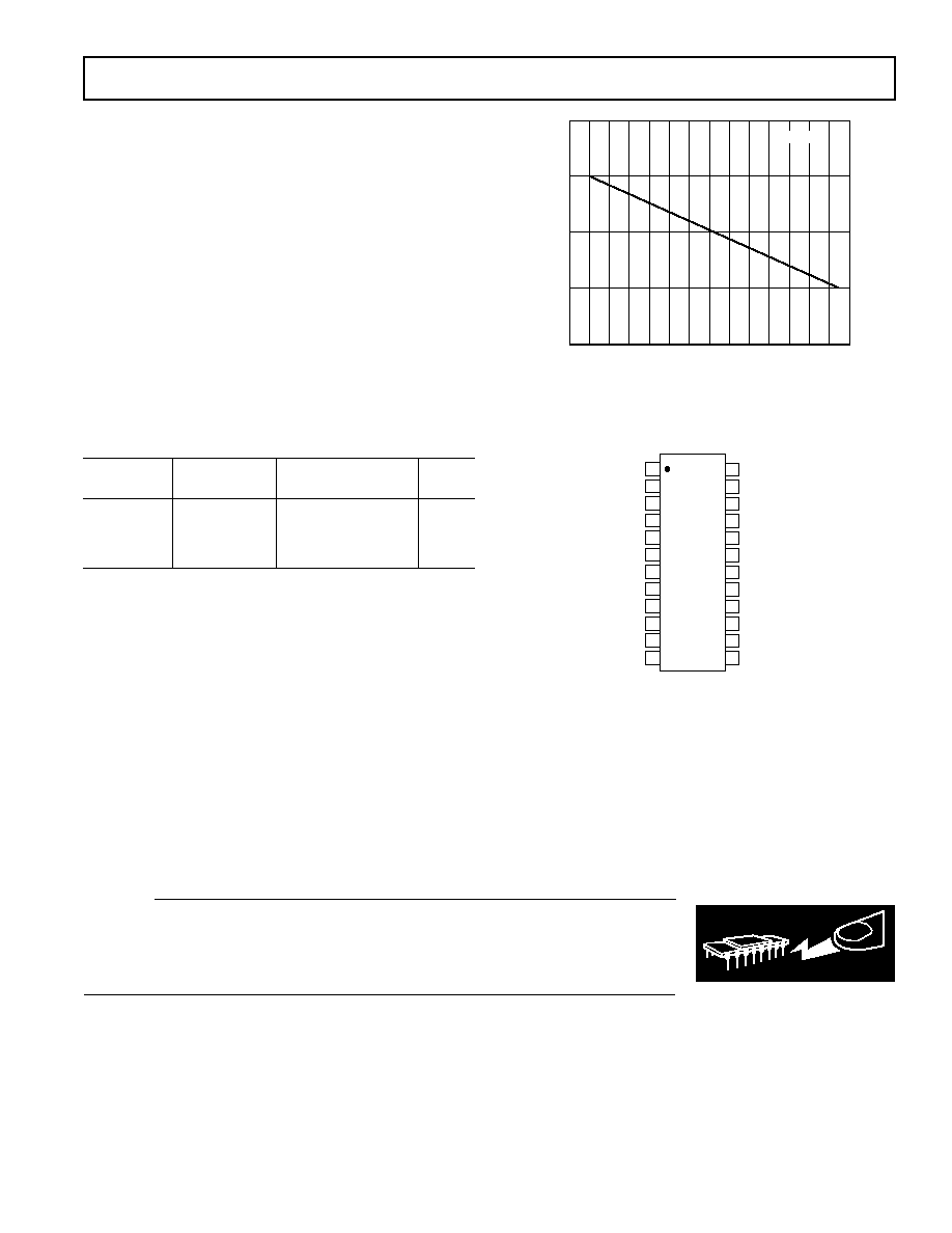
MAXIMUM POWER DISSIPATION
The maximum power that can be safely dissipated by the AD8183/
AD8185 is limited by the associated rise in junction temperature.
The maximum safe junction temperature for plastic encapsulated
devices is determined by the glass transition temperature of the
plastic, approximately 150
°
C. Temporarily exceeding this
limit may cause a shift in parametric performance due to a
change in the stresses exerted on the die by the package. Exceeding
a junction temperature of 175
°
C for an extended period can
result in device failure.
While the AD8183/AD8185 is internally short circuit protected,
this may not be sufficient to guarantee that the maximum junction
temperature (150
°
C) is not exceeded under all conditions. To
ensure proper operation, it is necessary to observe the maximum
power derating curves shown in Figure 2.
CAUTION
ESD (electrostatic discharge) sensitive device. Electrostatic charges as high as 4000 V readily
accumulate on the human body and test equipment and can discharge without detection.
Although the AD8183/AD8185 features proprietary ESD protection circuitry, permanent damage
may occur on devices subjected to high energy electrostatic discharges. Therefore, proper ESD
precautions are recommended to avoid performance degradation or loss of functionality.
WARNING!
ESD SENSITIVE DEVICE
AMBIENT TEMPERATURE C
2.0
50
MAXIMUM POWER DISSIPATION Watts
40 30 20 10
0
10 20
30
40 50
60 70
80
90
1.5
1.0
0
T
J
= 150 C
0.5
Figure 2. Maximum Power Dissipation vs. Temperature
PIN CONFIGURATION
TOP VIEW
(Not to Scale)
24
23
22
21
20
19
18
17
16
15
14
13
1
2
3
4
5
6
7
8
9
10
11
12
AD8183/
AD8185
IN0A
V
CC
DGND
OE
IN1A
SEL
A
/B
GND
V
CC
IN2A
OUT0
V
CC
V
EE
V
EE
OUT1
IN2B
V
CC
GND
OUT2
IN1B
V
EE
GND
DVCC
IN0B
V
CC
REV. 0
AD8183/AD8185
4
FREQUENCY MHz
1
0.1
GAIN dB
0
1
2
3
4
5
6
7
8
9
1
10
100
1k
GAIN
FLATNESS
V
O
AS SHOWN
R
L
= 150
200mV p-p
2V p-p
200mV p-p
2V p-p
0.1
0
0.1
0.2
0.3
0.4
0.5
0.6
FLATNESS dB
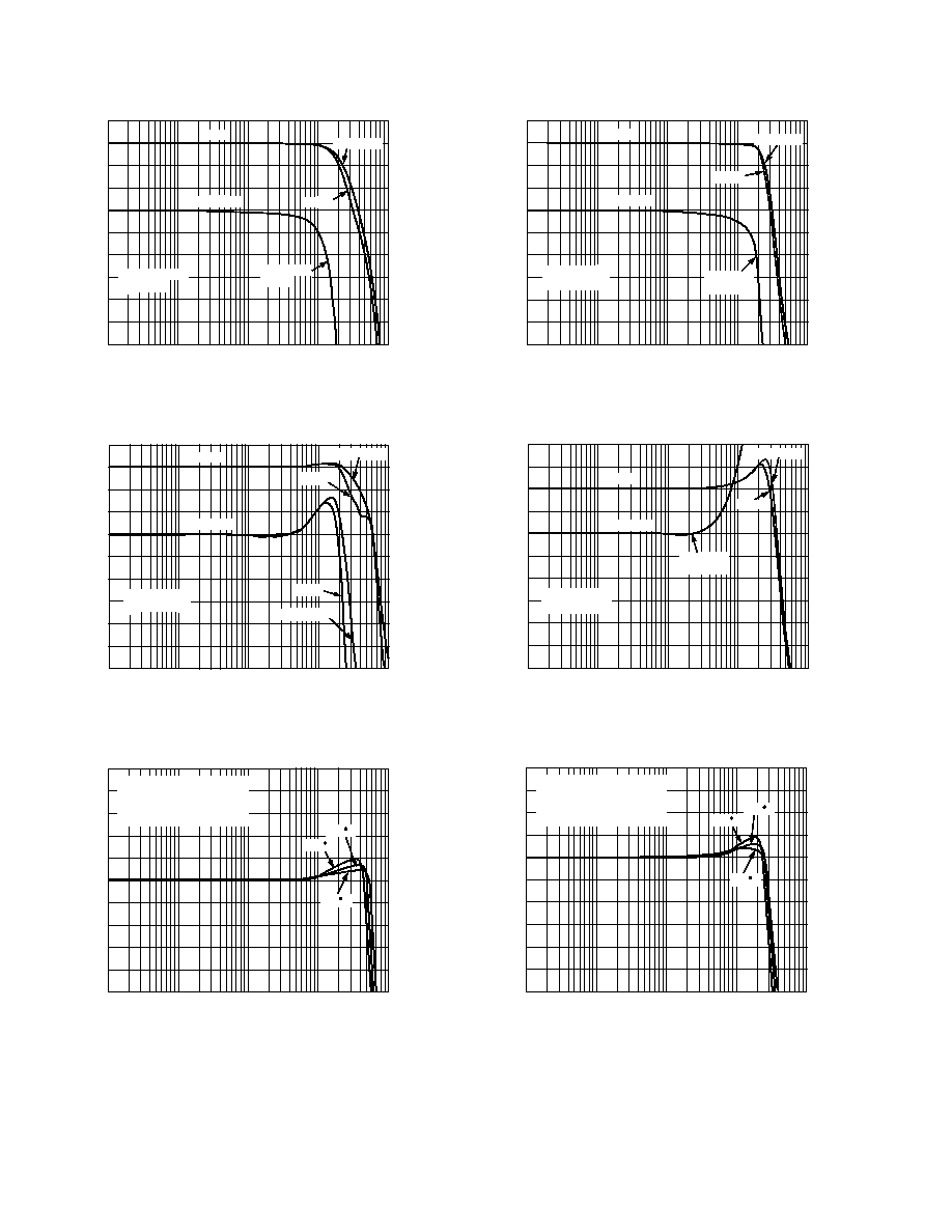
Figure 3. AD8183 Frequency Response; R
L
= 150
FREQUENCY MHz
1
0.1
GAIN dB
0
1
2
3
4
5
6
7
8
9
1
10
100
1k
GAIN
FLATNESS
V
O
AS SHOWN
R
L
= 1k
200mV p-p
2V p-p
200mV p-p
2V p-p
0.1
0
0.1
0.2
0.3
0.4
0.5
0.6
FLATNESS dB
0.2
0.3
Figure 4. AD8183 Frequency Response; R
L
= 1 k
FREQUENCY MHz
5
0.1
GAIN dB
4
3
2
1
0
1
2
3
4
5
1
10
100
1k
V
O
= 200mV p-p
R
L
= 1k
C
L
= 5pF
TEMPERATURE AS SHOWN
+85 C
+25 C
40 C
Figure 5. AD8183 Frequency Response vs. Temperature
FREQUENCY MHz
1
0.1
NORMALIZED GAIN dB
0
1
2
3
4
5
6
7
8
9
1
10
100
1k
GAIN
FLATNESS
V
O
AS SHOWN
R
L
= 150
200mV p-p
2V p-p
200mV p-p
2V p-p
0.1
0
0.1
0.2
0.3
0.4
0.5
0.6
NORMALIZED FLATNESS dB
Figure 6. AD8185 Frequency Response; R
L
= 150
FREQUENCY MHz
2
0.1
NORMALIZED GAIN dB
1
0
1
2
3
4
5
6
7
8
1
10
100
1k
GAIN
FLATNESS
V
O
AS SHOWN
R
L
= 1k
200mV p-p
2V p-p
200mV p-p
2V p-p
0.1
0
0.1
0.2
0.3
0.4
0.5
0.6
NORMALIZED FLATNESS dB
0.2
0.3
Figure 7. AD8185 Frequency Response; R
L
= 1 k
FREQUENCY MHz
4
0.1
NORMALIZED GAIN dB
3
2
1
0
1
2
3
4
5
6
1
10
100
1k
V
O
= 200mV p-p
R
L
= 150
C
L
= 5pF
TEMPERATURE AS SHOWN
+85 C
+25 C
40 C
Figure 8. AD8185 Frequency Response vs. Temperature
REV. 0
AD8183/AD8185
5
FREQUENCY MHz
10
1
CROSSTALK dB
20
30
40
50
60
70
80
90
100
110
10
100
1k
R
L
= 1k
R
T
= 37.5
ALL-HOSTILE
ADJACENT
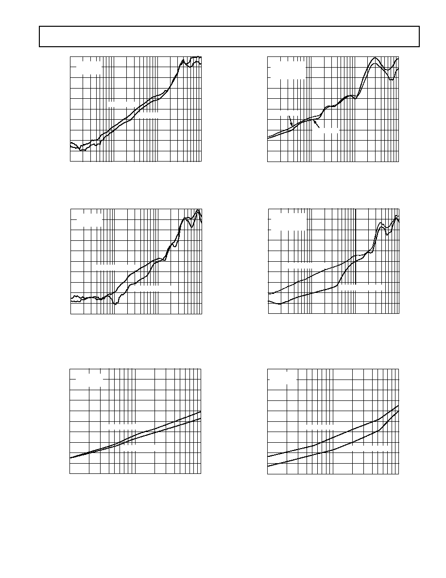
Figure 9. AD8183 Crosstalk vs. Frequency
FREQUENCY MHz
10
1
CHANNEL-TO-CHANNELCROSSTALK dB
20
30
40
50
60
70
80
90
100
110
10
100
1k
R
L
= 1k
R
T
= 37.5
DRIVE B, LISTEN A
DRIVE A, LISTEN B
Figure 10. AD8183 Channel-to-Channel Crosstalk vs.
Frequency
FUNDAMENTAL FREQUENCY MHz
0
1
DISTORTION dBc
10
20
30
40
50
60
70
80
90
100
10
100
V
O
= 2V p-p
R
L
= 150
SECOND HARMONIC
THIRD HARMONIC
Figure 11. AD8183 Distortion vs. Frequency
FREQUENCY MHz
10
1
CROSSTALK dB
20
30
40
50
60
70
80
90
100
110
10
100
1k
R
L
= 150
R
T
= 37.5
RTI MEASURED
ALL-HOSTILE
ADJACENT
Figure 12. AD8185 Crosstalk vs. Frequency
FREQUENCY MHz
10
1
CHANNEL-TO-CHANNEL CROSSTALK dB
20
30
40
50
60
70
80
90
100
110
10
100
1k
R
L
= 150
R
T
= 37.5
RTI MEASURED
DRIVE A, LISTEN B
DRIVE B, LISTEN A
Figure 13. AD8185 Channel-to-Channel Crosstalk vs.
Frequency
FUNDAMENTAL FREQUENCY MHz
0
1
DISTORTION dBc
10
20
30
40
50
60
70
80
90
100
10
100
V
O
= 2V p-p
R
L
= 150
SECOND HARMONIC
THIRD HARMONIC
Figure 14. AD8185 Distortion vs. Frequency