REV. 0
Information furnished by Analog Devices is believed to be accurate and
reliable. However, no responsibility is assumed by Analog Devices for its
use, nor for any infringements of patents or other rights of third parties
which may result from its use. No license is granted by implication or
otherwise under any patent or patent rights of Analog Devices.
a
Dual, 16 MHz, Rail-to-Rail
FET Input Amplifier
AD823
© Analog Devices, Inc., 1995
One Technology Way, P.O. Box 9106, Norwood. MA 02062-9106, U.S.A.
Tel: 617/329-4700
Fax: 617/326-8703
FEATURES
Single Supply Operation
Output Swings Rail to Rail
Input Voltage Range Extends Below Ground
Single Supply Capability from +3 V to +36 V
High Load Drive
Capacitive Load Drive of 500 pF, G = +1
Output Current of 15 mA, 0.5 V from Supplies
Excellent AC Performance on 2.6 mA/Amplifier
≠3 dB Bandwidth of 16 MHz, G = +1
350 ns Settling Time to 0.01% (2 V Step)
Slew Rate of 22 V/ s
Good DC Performance
800 V Max Input Offset Voltage
2 V/ C Offset Voltage Drift
25 pA Max Input Bias Current
Low Distortion
≠108 dBc Worst Harmonic @ 20 kHz
Low Noise
16 nV/
Hz @ 10 kHz
No Phase Inversion with Inputs to the Supply Rails
APPLICATIONS
Battery Powered Precision Instrumentation
Photodiode Preamps
Active Filters
12- to 16-Bit Data Acquisition Systems
Medical Instrumentation
CONNECTION DIAGRAM
8-Pin Plastic Mini-DIP
and
8-Lead SOIC
1
2
3
4
8
7
6
5
AD823
OUT1
+IN2
≠IN2
OUT2
+V
S
≠IN1
+IN1
≠V
S
PRODUCT DESCRIPTION
The AD823 is a dual precision, 16 MHz, JFET input op amp
that can operate from a single supply of +3.0 V to +36 V, or
dual supplies of
±
1.5 V to
±
18 V. It has true single supply
capability with an input voltage range extending below ground
in single supply mode. Output voltage swing extends to within
50 mV of each rail for I
OUT
100
µ
A providing outstanding out-
put dynamic range.
Offset voltage of 800
µ
V max, offset voltage drift of 2
µ
V/
∞
C,
input bias currents below 25 pA and low input voltage noise
provide dc precision with source impedances up to a Gigohm.
16 MHz, ≠3 dB bandwidth, ≠108 dB THD @ 20 kHz and
22 V/
µ
s slew rate are provided with a low supply current of
2.6 mA per amplifier. The AD823 drives up to 500 pF of direct
capacitive load as a follower, and provides an output current of
15 mA, 0.5 V from the supply rails. This allows the amplifier to
handle a wide range of load conditions.
This combination of ac and dc performance, plus the outstand-
ing load drive capability results in an exceptionally versatile am-
plifier for applications such as A/D drivers, high-speed active
filters, and other low voltage, high dynamic range systems.
The AD823 is available over the industrial temperature range of
≠40
∞
C to +85
∞
C and is offered in both 8-pin plastic DIP and
SOIC packages.
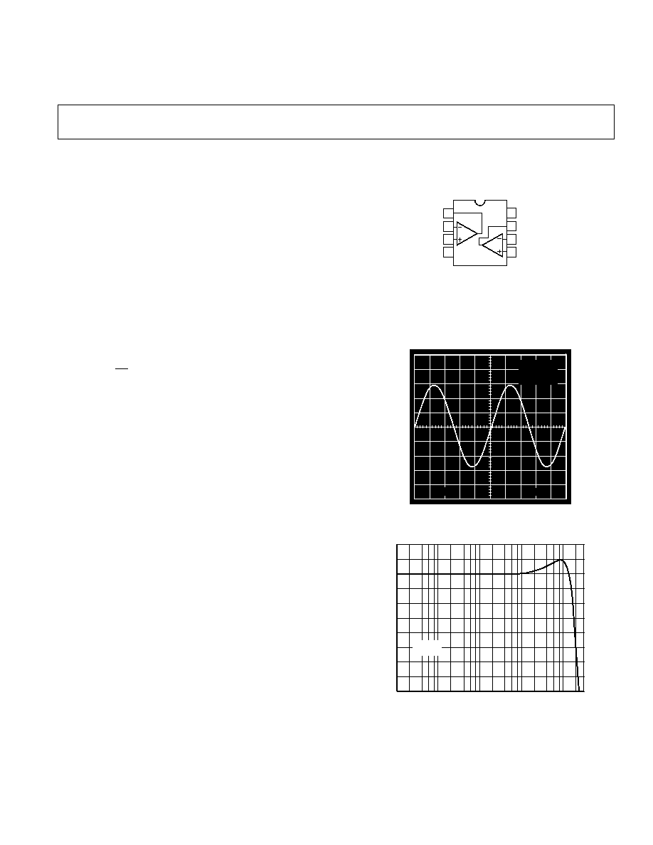
3V
GND
R
L
= 100k
C
L
= 50pF
V
S
= +3V
200µs
500mV
Figure 1. Output Swing, V
S
= +3 V, G = +1
FREQUENCY ≠ Hz
≠8
OUTPUT ≠ dB
1k
≠6
≠7
2
1
10k
100k
1M
V
S
= +5V
G = +1
≠5
≠4
≠3
≠2
≠1
0
10M
Figure 2. Small Signal Bandwidth, G = +1

AD823A
Parameter
Conditions
Min
Typ
Max
Units
DYNAMIC PERFORMANCE
≠3 dB Bandwidth, V
O
0.2 V p-p
G = +1
12
16
MHz
Full Power Response
V
O
= 2 V p-p
3.5
MHz
Slew Rate
G = ≠1, V
O
= 4 V Step
14
22
V/
µ
s
Settling Time
G = ≠1, V
O
= 2 V Step
to 0.1%
320
ns
to 0.01%
350
ns
NOISE/DISTORTION PERFORMANCE
Input Voltage Noise
f = 10 kHz
16
nV/
Hz
Input Current Noise
f = 1 kHz
1
fA/
Hz
Harmonic Distortion
R
L
= 600
to 2.5 V, V
O
= 2 V p-p,
≠108
dBc
f = 20 kHz
Crosstalk
f = 1 kHz
R
L
= 5 k
≠130
dB
f = 1 MHz
R
L
= 5 k
≠93
dB
DC PERFORMANCE
Initial Offset
0.2
0.8
mV
Max Offset Over Temperature
0.3
2.0
mV
Offset Drift
2
µ
V/
∞
C
Input Bias Current
V
CM
= 0 V to +4 V
3
25
pA
at T
MAX
0.5
5
nA
Input Offset Current
2
20
pA
at T
MAX
0.5
nA
Open-Loop Gain
V
O
= 0.2 V to 4 V
R
L
= 2 k
20
45
V/mV
T
MIN
to T
MAX
20
V/mV
INPUT CHARACTERISTICS
Input Common-Mode Voltage Range
≠0.2 to 3 ≠0.2 to 3.8
V
Input Resistance
10
13
Input Capacitance
1.8
pF
Common-Mode Rejection Ratio
V
CM
= 0 V to 3 V
60
76
dB
OUTPUT CHARACTERISTICS
Output Voltage Swing
I
L
=
±
100
µ
A
0.025 to 4.975
V
I
L
=
±
2 mA
0.08 to 4.92
V
I
L
=
±
10 mA
0.25 to 4.75
V
Output Current
V
OUT
= 0.5 V to 4.5 V
16
mA
Short Circuit Current
Sourcing to 2.5 V
40
mA
Sinking to 2.5 V
30
mA
Capacitive Load Drive
G = +1
500
pF
POWER SUPPLY
Operating Range
+3
+36
V
Quiescent Current
T
MIN
to T
MAX
, Total
5.2
5.6
mA
Power Supply Rejection Ratio
V
S
= +5 V to +15 V, T
MIN
to T
MAX
70
80
dB
Specification subject to change without notice.
REV. 0
≠2≠
(@ T
A
= +25
∞
C, V
S
= +5 V, R
L
= 2 k
to +2.5 V, unless otherwise noted)
AD823≠SPECIFICATIONS

AD823
REV. 0
≠3≠
AD823A
Parameter
Conditions
Min
Typ
Max
Units
DYNAMIC PERFORMANCE
≠3 dB Bandwidth, V
O
0.2 V p-p
G = +1
12
15
MHz
Full Power Response
V
O
= 2 V p-p
3.2
MHz
Slew Rate
G = ≠1, V
O
= 2 V Step
13
20
V/
µ
s
Settling Time
G = ≠1, V
O
= 2 V Step
to 0.1%
250
ns
to 0.01%
300
ns
NOISE/DISTORTION PERFORMANCE
Input Voltage Noise
f = 10 kHz
16
nV/
Hz
Input Current Noise
f = 1 kHz
1
fA/
Hz
Harmonic Distortion
R
L
= 100
, V
O
= 2 V p-p, f = 20 kHz
≠93
dBc
Crosstalk
f = 1 kHz
R
L
= 5 k
≠130
dB
f = 1 MHz
R
L
= 5 k
≠93
dB
DC PERFORMANCE
Initial Offset
0.2
1.5
mV
Max Offset Over Temperature
0.5
2.5
mV
Offset Drift
2
µ
V/
∞
C
Input Bias Current
V
CM
= 0 V to +2 V
3
25
pA
at T
MAX
0.5
5
nA
Input Offset Current
2
20
pA
at T
MAX
0.5
nA
Open-Loop Gain
V
O
= 0.2 V to 2 V
R
L
= 2 k
15
30
V/mV
T
MIN
to T
MAX
12
V/mV
INPUT CHARACTERISTICS
Input Common-Mode Voltage Range
≠0.2 to 1 ≠0.2 to 1.8
V
Input Resistance
10
13
Input Capacitance
1.8
pF
Common-Mode Rejection Ratio
V
CM
= 0 V to 1 V
54
70
dB
OUTPUT CHARACTERISTICS
Output Voltage Swing
I
L
=
±
100
µ
A
0.025 to 3.275
V
I
L
=
±
2 mA
0.08 to 3.22
V
I
L
=
±
10 mA
0.25 to 3.05
V
Output Current
V
OUT
= 0.5 V to 2.5 V
15
mA
Short Circuit Current
Sourcing to 1.5 V
40
mA
Sinking to 1.5 V
30
mA
Capacitive Load Drive
G = +1
500
pF
POWER SUPPLY
Operating Range
+3
+36
V
Quiescent Current
T
MIN
to T
MAX
, Total
5.0
5.7
mA
Power Supply Rejection Ratio
V
S
= +3.3 V to +15 V, T
MIN
to T
MAX
70
80
dB
Specification subject to change without notice.
SPECIFICATIONS
(@ T
A
= +25
∞
C, V
S
= +3.3 V, R
L
= 2 k
to +1.65 V, unless otherwise noted)

AD823A
Parameter
Conditions
Min
Typ
Max
Units
DYNAMIC PERFORMANCE
≠3 dB Bandwidth, V
O
0.2 V p-p
G = +1
12
16
MHz
Full Power Response
V
O
= 2 V p-p
4
MHz
Slew Rate
G = ≠1, V
O
= 10 V Step
17
25
V/
µ
s
Settling Time
G = ≠1, V
O
= 10 V Step
to 0.1%
550
ns
to 0.01%
650
ns
NOISE/DISTORTION PERFORMANCE
Input Voltage Noise
f = 10 kHz
16
nV/
Hz
Input Current Noise
f = 1 kHz
1
fA/
Hz
Harmonic Distortion
R
L
= 600
, V
O
= 10 V p-p,
≠90
dBc
f = 20 kHz
Crosstalk
f = 1 kHz
R
L
= 5 k
≠130
dB
f = 1 MHz
R
L
= 5 k
≠93
dB
DC PERFORMANCE
Initial Offset
0.7
3.5
mV
Max Offset Over Temperature
1.0
7
mV
Offset Drift
2
µ
V/
∞
C
Input Bias Current
V
CM
= 0 V
5
30
pA
V
CM
= ≠10 V
60
pA
at T
MAX
V
CM
= 0 V
0.5
5
nA
Input Offset Current
2
20
pA
at T
MAX
0.5
nA
Open-Loop Gain
V
O
= +10 V to ≠10 V
R
L
= 2 k
30
60
V/mV
T
MIN
to T
MAX
30
V/mV
INPUT CHARACTERISTICS
Input Common-Mode Voltage Range
≠15.2 to 13
≠15.2 to 13.8
V
Input Resistance
10
13
Input Capacitance
1.8
pF
Common-Mode Rejection Ratio
V
CM
= ≠15 V to +13 V
66
82
dB
OUTPUT CHARACTERISTICS
Output Voltage Swing
I
L
=
±
100
µ
A
≠14.95 to +14.95
V
I
L
=
±
2 mA
≠14.92 to +14.92
V
I
L
=
±
10 mA
≠14.75 to +14.75
V
Output Current
V
OUT
= ≠14.5 V to +14.5 V
17
mA
Short Circuit Current
Sourcing to 0 V
80
mA
Sinking to 0 V
60
mA
Capacitive Load Drive
G = +1
500
pF
POWER SUPPLY
Operating Range
+3
+36
V
Quiescent Current
T
MIN
to T
MAX
, Total
7.0
8.4
mA
Power Supply Rejection Ratio
V
S
= +5 V to +15 V, T
MIN
to T
MAX
70
80
dB
Specification subject to change without notice.
REV. 0
≠4≠
AD823≠SPECIFICATIONS
(@ T
A
= +25
∞
C, V
S
=
±
15 V, R
L
= 2 k
to 0 V, unless otherwise noted)

AD823
REV. 0
≠5≠
ABSOLUTE MAXIMUM RATINGS
1
Supply Voltage . . . . . . . . . . . . . . . . . . . . . . . . . . . . . . . . +36 V
Internal Power Dissipation
2
Plastic Package (N) . . . . . . . . . . . . . . . . . . . . . . . . 1.3 Watts
Small Outline Package (R) . . . . . . . . . . . . . . . . . . . 0.9 Watts
Input Voltage (Common Mode) . . . . . . . . . . . . . . . . . . . .
±
V
S
Differential Input Voltage . . . . . . . . . . . . . . . . . . . . . . .
±
1.2 V
Output Short Circuit Duration
. . . . . . . . . . . . . . . . . . . . . . Observe Power Derating Curves
Storage Temperature Range N, R . . . . . . . . . ≠65
∞
C to +125
∞
C
Operating Temperature Range . . . . . . . . . . . . ≠ 40
∞
C to +85
∞
C
Lead Temperature Range (Soldering 10 sec) . . . . . . . . +300
∞
C
NOTES
1
Stresses above those listed under "Absolute Maximum Ratings" may cause
permanent damage to the device. This is a stress rating only and functional
operation of the device at these or any other conditions above those indicated in the
operational section of this specification is not implied. Exposure to absolute
maximum rating conditions for extended periods may affect device reliability.
2
Specification is for device in free air:
8-Pin Plastic Package:
JA
= 90
∞
C/Watt
8-Pin SOIC Package:
JA
= 160
∞
C/Watt
ORDERING GUIDE
Model
Temperature Range
Package Description
Package Option
AD823AN
≠ 40
∞
C to +85
∞
C
8-Pin Plastic DIP
N-8
AD823AR
≠ 40
∞
C to +85
∞
C
8-Pin Plastic SOIC
SO-8
AD823AR-REEL
≠ 40
∞
C to +85
∞
C
SOIC on Reel
SO-8
MAXIMUM POWER DISSIPATION ≠ Watts
AMBIENT TEMPERATURE ≠
∞
C
2.0
1.5
0
≠50
90
≠40 ≠30 ≠20 ≠10
0
10
20
30
50
60
70
80
40
1.0
0.5
8-PIN MINI-DIP PACKAGE
8-PIN SOIC PACKAGE
T
J
= +150
∞
C
Figure 3. Maximum Power Dissipation vs. Temperature
WARNING!
ESD SENSITIVE DEVICE
CAUTION
ESD (electrostatic discharge) sensitive device. Electrostatic charges as high as 4000 V readily
accumulate on the human body and test equipment and can discharge without detection.
Although the AD823 features proprietary ESD protection circuitry, permanent damage may
occur on devices subjected to high energy electrostatic discharges. Therefore, proper ESD
precautions are recommended to avoid performance degradation or loss of functionality.